
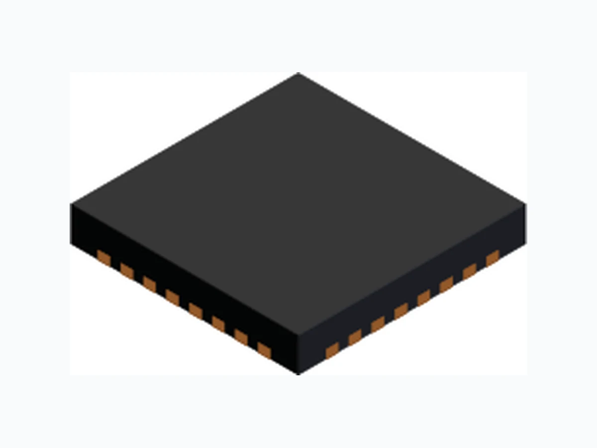
A4923 ALLEGRO
Document overview
- Manufacturer or author: Provided By www.digicamel.com(FREE DATASHEET DOWNLOAD SITE)
- PDF pages: 11
Technical content
NOTE: For detailed information on purchasing options, contact your local Allegro field applications engineer or sales representative. Allegro MicroSystems, LLC reserves the right to make, from time to time, revisions to the anticipated product life cycle plan for a product to accommodate changes in production capabilities, alternative product availabilities, or market demand. The information included herein is believed to be accurate and reliable. However, Allegro MicroSystems, LLC assumes no respon- sibility for its use; nor for any infringements of patents or other rights of third parties which may result from its use. 3-Phase Sinusoidal Motor Controller A4923 Date of status change: January 20, 2016 These parts are no longer in production The device should not be purchased for new design applications. Samples are no longer available. Discontinued Product
Description
Designed to control three-phase brushless DC motors, the A4923 is capable of high-current gate drive for an all N-channel power MOSFET 3-phase bridge. Sinusoidal current control is employed via output PWM, to minimize vibration, noise, and torque ripple. Internal circuit protection includes thermal shutdown with hysteresis, over-current, and dead-time protection. Special power up sequencing is not required. The A4923 is supplied in a 32 terminal 5×5×0.9mm QFN package (suffix ET) with exposed pad for enhanced thermal dissipation. This small footprint package is lead (Pb) free with 100% matte tin leadframe plating, and it is also available with optional sidewall plating. A4923-DS Features and Benefits
- Sinusoidal Drive Current
- Hall Element Inputs
- PWM Current Limiting
- Dead-time Protection
- FGO (Tach) Output
- Internal UVLO
- Thermal Shutdown Circuitry 3-Phase Sinusoidal Motor Controller Packages: 32-Pin QFN (suffix ET) Typical Application Diagram Not to scale A4923 External Control FGO Hall HC+ HC- Hall HB+ HB- Hall HA+ HA- STARTn BRAKE DIR GNDTEST1 TEST2 BLDC Motor Rsense LSS A4923 GLC GLB GLA CP1 SC SB SA CP2 GHC GHB GHA Phase A Phase B Phase C VCP VBB VBBVREG7.2 VREG3.3
3-Phase Sinusoidal Motor ControllerA4923 Allegro MicroSystems, LLC
115 Northeast Cutoff
Worcester, Massachusetts 01615-0036 U.S.A. Absolute Maximum Ratings Characteristic Symbol Notes Rating Unit Supply Voltage VBB 36 V Logic Input Voltage Range VIN –0.3 to 6 V Logic Outputs VO 6 V Junction Temperature TJ 150 °C Operating Ambient Temperature Range TA Range G –40 to 105 °C Storage Temperature Range Tstg –55 to 150 °C Thermal Characteristics may require derating at maximum conditions, see application information Characteristic Symbol Test Conditions* Value Unit Package Thermal Resistance A4923GET RθJA On 2-sided PCB, 1 in2 copper 50 ºC/W On 4-layer PCB 32 ºC/W *Additional thermal information available on the Allegro website. Selection Guide Part Number Package Packing Sidewall Plating A4923GETTR-T 5 mm X 5 mm, 0.90 mm nominal height QFN 1500 pieces per reel No A4923GETTR-R* 5 mm X 5 mm, 0.90 mm nominal height QFN 1500 pieces per reel Yes *Contact factory for availability
3-Phase Sinusoidal Motor ControllerA4923 Allegro MicroSystems, LLC Worcester, Massachusetts 01615-0036 U.S.A. Terminal List Table Name Function Number Name Function Number HC- Analog hall input C 1 SC High-side source connection C 17 HA+ Analog hall input A 2 GLC Low-side gate drive C 18 HB+ Analog hall input B 3 GLB Low-side gate drive B 19 HC+ Analog hall input C 4 GLA Low-side gate drive A 20 VREG3.3 3.3V regulator capacitor terminal 5 LSS Low-side sense resistor connection 21 GND Ground 6 – No connect 22 VREG7.2 7.2V regulator capacitor terminal 7 – No connect 23 CP1 Charge pump capacitor terminal 8 – No connect 24 CP2 Charge pump capacitor terminal 9 STARTn Digital start input 25 VCP Charge pump reservoir cap terminal 10 DIR Digital direction input 26 VBB Supply voltage 11 BRAKE Digital brake input 27 GHA High-side gate drive A 12 TEST1 ATE terminal, can be left open or connected to GND SA High-side source connection A 13 FGO Digital motor-speed output 29 GHB High-side gate drive B 14 TEST2 ATE terminal, can be left open or connected to GND SB High-side source connection B 15 HA- Analog hall input A 31 GHC High-side gate drive C 16 HB- Analog hall input B 32 PAD - 1HC- PAD CP2
24 No Connect
32 HB-
23 No Connect
31 HA-
22 No Connect
30 TEST2
21 LSS
29 FGO
5VREG3.3 SA
20 GLA
28 TEST1
19 GLB
27 BRAKE
7VREG7.2 SB
18 GLC
26 DIR
25 STARTn
3-Phase Sinusoidal Motor ControllerA4923 Allegro MicroSystems, LLC Worcester, Massachusetts 01615-0036 U.S.A. ELECTRICAL CHARACTERISTICS Valid at TA = 25°C, unless otherwise specified Characteristic Symbol Test Conditions Min. Typ. Max. Unit Supply and Reference VBB Voltage Range VBB 10 – 32 V VBB Supply Current IBB – 18 22 mA VREG7.2 Current Limit ILIMREG7.2 –30 – – mA Logic Inputs STARTn, DIR, BRAKE Logic Input Low Level VIL 0 – 0.8 V Logic Input High Level VIH 2.0 – 5.5 V Logic Input Hysteresis VHYS – 350 – kHz Logic Input Current RIN Pull-up to internal 3.3V 34 47 60 kΩ IIN(1) VIN = 5 V – 36 – µA IIN(0) VIN = 0 V – –70 – µA Logic Outputs FGO Output Saturation Voltage VSAT I = -7 mA – 0.14 0.21 V Output Leakage IFGO V = 3.3 V – – 1 µA Halls Hall Input Current IHALL VIN = 0.2 V to 3.4 V –1 0 1 µA Common Mode Input Range VCMR 0.2 – 3.4 V AC Input Voltage Range VHALL 50 – – mVp-p Hall Digital Filter Time tHALL – 1.6 – µs Gate Drive PWM Carrier Frequency fPWM 19 20 21 kHz Current Limit Input Threshold VLSS Threshold on LSS terminal 216 240 256 mV Gate Drive Output Voltage VGS IGATE = -2 mA 6.0 6.9 – V Gate Drive Source Current IGSRC VGX = 4 V -21 -30 -39 mA Gate Drive Sink Current IGSNK VGX = 4 V 50 70 90 mA Gate Pulldown, Passive RPULLDOWN – 300 – kΩ Dead Time tDEAD 1460 – 1880 µs Fixed Off-time tOFF 21.0 – 27.5 µs LSS Digital Filter Time tBLANK 720 – 880 µs Protection Thermal Shutdown Temperature TJTSD – 130 – °C Thermal Shutdown Hysteresis DTJTSD – 10 – °C VBB UVLO Threshold VUVLO Rising VBB – 7.0 7.85 V VBB UVLO Hysteresis VUVLOHYST 0.5 0.75 1.0 V NOTES: 1. Typical Data is for design information only. 2. Negative current is defined as coming out of (sourcing) the specified device terminal. 3. Specifications over operating temperature range are assured by design and characterization.
3-Phase Sinusoidal Motor ControllerA4923 Allegro MicroSystems, LLC Worcester, Massachusetts 01615-0036 U.S.A. Hall Time Filter Sine Drive PWM Generation Trap Decode Direction Detection Driver Control Mode Selection Reg 7.2 V VReg7.2 Reg 3.3 V VReg3.3 VBB Monitor Charge Pump 20 kHz PWM Dead Time Time Filter + FGO HC+ HC- HALL A, B, C HB+ HB- HA+ HA- STARTn BRAKE DIR TEST1 TEST2 GND LSS 1.2 V GLC GLB GLA CP1 SC SB SA CP2 GHC GHB GHA VCP VBB VBB Reg 7.2 V OVER- CURRENT Parallel Control Register
2.5 MHz OSC 40 MHz PLL
3-Phase Sinusoidal Motor ControllerA4923 Allegro MicroSystems, LLC Worcester, Massachusetts 01615-0036 U.S.A. Functional Description STARTn The STARTn terminal is the active-low start/stop logic input. (low = start, high = all gate drive outputs off). Internally pulled up to VREG3.3. BRAKE The BRAKE terminal is the active-high logic input to turn on all low-side MOSFETs. The STARTn terminal must be active (low) to enable brake. Internally pulled up to VREG3.3 DIR The DIR terminal is the logic input to control the motor’s direc- tion. A logic high = FWD and a logic low = REV . Internally pulled up to VREG3.3. Table 1: STARTn BRAKEn Fault Function H X L All gate outputs low L L L Run L H L Brake X X H All gate outputs low FGO The FGO terminal is an open-drain logic output which toggles state each hall transition. TEST1, TEST2 The TEST1 and TEST2 terminals are for ATE testing and can be left open or tied to GND. Current Limit Over-current is controlled by an internal fixed off-time PWM control circuit. At the trip point, the sense comparator turns off the enabled low-side driver, turns on the corresponding high side driver, and the motor current recirculates through the high-side drivers. ITRIP = 240 mV / RSENSE Hall Inputs Unique circuitry incorporates hysteresis which toggles polarity with the hall input slope direction. This allows the hall com- parators to operate with very small offsets and results in highly symmetrical comparator outputs. A digital filter on the hall inputs minimizes sensitivity to noise. VPOS A 0.1 μF capacitor is required between this terminal and GND to stabilize the internal 3.3 V regulator VREG A 0.1 μF capacitor is required between this terminal and GND to stabilize the low-side gate supply. Charge Pump Terminals CP1, CP2, and VCP generate a voltage above VBB that is used for the high-side gate supply. A 0.1 μF capacitor is required between the CP1 and CP2 terminals, and between VCP and VBB. Fault A fault occurs when VBB, the charge pump, or HBIAS falls below the respective UVLO threshold, the device temperature rises above TJ, or the hall inputs indicate an invalid state (111 or 000). The outputs are disabled in the event of a fault. Faults are not latched, and the device resumes operation once the fault is cleared.
3-Phase Sinusoidal Motor ControllerA4923 Allegro MicroSystems, LLC Worcester, Massachusetts 01615-0036 U.S.A. Sine Mode When the motor is stopped, a Hall Timeout error exists since the hall-transition timer has timed out. When a start signal is applied via the STARTn terminal, the motor is enabled in trapezoidal mode. When two consecutive hall transitions do not overflow the hall-transition timer, the Hall Timeout error is cleared and the drive switches to sinusoidal mode. The sine modulation profile is stored in a digital look-up table. The sine modulation value is updated from the profile 192 times per electrical revolution. At each hall transition, which occurs every 60° or every 32 steps, the profile index is forced to the appropriate step. It is then advanced the successive 32 steps with a timer set internally using the previous hall transition period. The motor outputs are generated as follows (phase advance is not shown to simplify this diagram): 60º 60º60º 60º60º 60º60º 60º60º 60º60º 60º HA Forward Reverse Motor Position from Hall Inputs Trapezoidal Drive (startup) - Motor Terminal Voltage Sine Drive - Internal Sine Modulation Signal SA SA HB SB SB HC SC SC Figure 1: Motor Outputs
3-Phase Sinusoidal Motor ControllerA4923 Allegro MicroSystems, LLC Worcester, Massachusetts 01615-0036 U.S.A. The internal sine modulation signal is converted to a PWM signal to drive the motor terminals. A 20 kHz carrier is modulated with the current sine profile value and used to generate the gate drive signals. Thus, the motor terminal voltage is a 20 kHz PWM sig- nal with a duty cycle dependent upon the sine modulation signal. The high- and low-side gate drivers on a given motor terminal are enabled inverted of the other, with a dead-time added to ensure both drivers will never be enabled at the same time. For increased efficiency, torque ripple, and audible noise, the sine profile is advanced 7.5º of one electrical revolution, relative to the hall transitions.
64 Steps 64 Steps 64 Steps
6 Bits of
VREG7.2 VBB Sine Drive Modulation Signal High-side Gate Drive Low-side Gate Drive Motor Terminal Voltage Figure 2: Sine Modulation Signal
3-Phase Sinusoidal Motor ControllerA4923 Allegro MicroSystems, LLC Worcester, Massachusetts 01615-0036 U.S.A. Package ET, 32-Pin QFN with Exposed Thermal Pad A A Terminal #1 mark area B Exposed thermal pad (reference only, terminal #1 identifier appearance at supplier discretion) For Reference Only; not for tooling use (reference JEDEC MO-220VHHD-5) Dimensions in millimeters Exact case and lead configuration at supplier discretion within limits shown C Reference land pattern layout (reference IPC7351 QFN50P500X500X100-33V6M); All pads a minimum of 0.20 mm from all adjacent pads; adjust as necessary to meet application process requirements and PCB layout tolerances; when mounting on a multilayer PCB, thermal vias at the exposed thermal pad land can improve thermal dissipation (reference EIA/JEDEC Standard JESD51-5) B PCB Layout Reference View 3.40 3.40
0.50 BSC
5.00 ±0.05 5.00 ±0.05 -0.07 0.40 ±0.10 3.40 3.40 0.30 0.50 1.00 5.00 5.00 C C0.08 33X SEATING PLANE CD D Coplanarity includes exposed thermal pad and terminals For the sidewall plating PCB footprint, see: http://www.allegromicro.com/en/Design-Center/Packaging.aspx
3-Phase Sinusoidal Motor ControllerA4923 Allegro MicroSystems, LLC Worcester, Massachusetts 01615-0036 U.S.A. Copyright ©2012-2014, Allegro MicroSystems, LLC Allegro MicroSystems, LLC reserves the right to make, from time to time, such departures from the detail specifications as may be required to permit improvements in the performance, reliability, or manufacturability of its products. Before placing an order, the user is cautioned to verify that the information being relied upon is current. Allegro’s products are not to be used in any devices or systems, including but not limited to life support devices or systems, in which a failure of Allegro’s product can reasonably be expected to cause bodily harm. The information included herein is believed to be accurate and reliable. However, Allegro MicroSystems, LLC assumes no responsibility for its use; nor for any infringement of patents or other rights of third parties which may result from its use.