
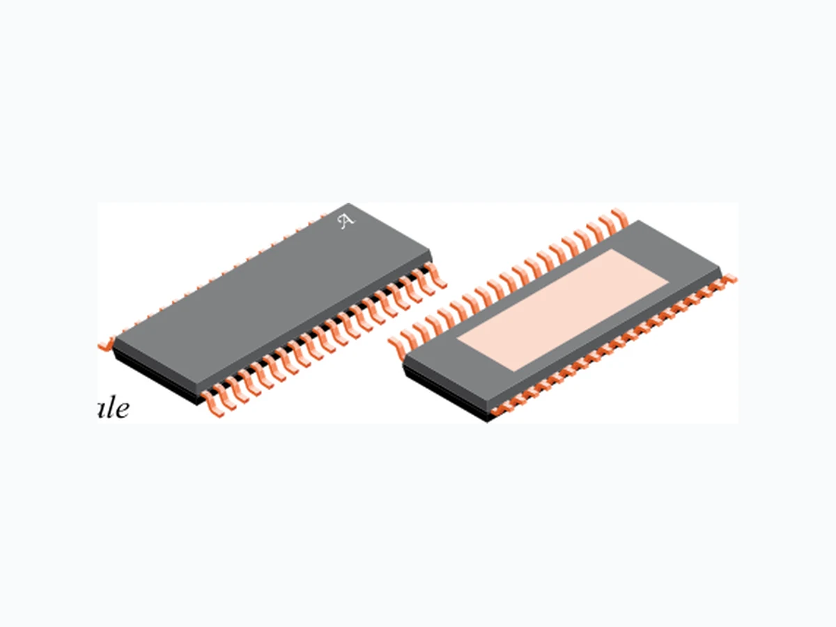
A4410 ALLEGRO
Document overview
- Manufacturer or author: Provided By www.digicamel.com(FREE DATASHEET DOWNLOAD SITE)
- PDF pages: 41
Technical content
The A4410 is power management IC that uses a buck or buck/ boost pre-regulator to efficiently convert automotive battery voltages into a tightly regulated intermediate voltage complete with control, diagnostics, and protections. The output of the pre-regulator supplies a 5 V/250 mA MAX tracking/protected LDO, a 3.3 V/160 mA MAX LDO, a 5 V/150 mA MAX LDO, and a 1.25 V/750 mADC/1 APEAK synchronous buck regulator. Designed to supply CAN or microprocessor power supplies in high temperature environments the A4410 is ideal for under hood applications. Enable inputs to the A4410 include a logic level (ENB) and two high-voltage (ENBAT1 and ENBAT2). The A4410 provides flexibility by including a TRACK pin to set the reference of the tracking regulator to either the 5 V or the 3.3 V output, so the A4410 can be adapted across multiple platforms with different sensors and supply rails. Diagnostic outputs from the A4410 include a power-on-reset output (NPOR) with a fixed 15 ms delay, an ENBAT1 and ENBAT2 status outputs, and a PowerOK output for the 5 V and 5 V protected LDOs (POK5V). Dual bandgaps, one for regulation and one for fault checking, improve long-term reliability of the A4410. The A4410 contains a Window Watchdog timer that can be programmed to accept a wide range of clock frequencies (WD ADJ). The watchdog timer has a fixed 30 ms activation delay to accommodate processor startup. The watchdog timer has an enable/disable pin (active LOW, WD ENn) to facilitate initial factory programming or field re-flash programming. Protection features include under and over voltage lockout on all four CPU supply rails. In case of a shorted output, all linear regulators feature fold back over current protection. In addition, the V5P output is protected from a short-to-battery event. Both A4410-DS
- Automotive AEC-Q100 qualified
- 2.8 VIN to 36 VIN operating range, 40 VIN maximum
- Buck or buck/boost pre-regulator (VREG)
- Adjustable PWM switching frequency: 250 kHz –
2.4 MHz
- PWM frequency can be synchronized to external clock
- 1.25 V/750 mADC/1 APEAK synchronous buck (1V25)
- 3.3 V (3V3) and 5 V (V5) internal LDO regulators with fold back short circuit protections
- 5 V (V5P) internal tracking LDO regulator with fold back short circuit and short-to-battery protections
- TRACK sets either 3V3 or V5 as the reference for V5P
- Power-on reset with fixed delay of 15 ms for 1V25/3V3 UV and OV protection (NPOR)
- Programmable watchdog timer with a 30 ms activation delay
- Active low, watchdog timer enable/disable pin (WD ENn)
- Dual band gaps for increased reliability: BGVREF, BGFAULT Adjustable Frequency Buck or Buck/Boost Pre-Regulator with a Synchronous Buck, 3 Internal LDOs, Window Watchdog Timer, and NPOR PACKAGE: 38-Pin eTSSOP (suffix LV) A4410 Simplified Block Diagram Not to scale A4410 5.35 V (VREG) Buck-Boost Pre-regulator
3.3 V LDO
(3V3) with Foldback Protection 1.25 V (1V25) Sync. Buck Regulator Programmable Pulse Width Watchdog Timer with Activation Delay Dual Bandgaps Charge Pump Thermal Shutdown (TSD) POK5V Output NPOR Output
5 V LDO
(V5) with Foldback Protection Tracking Control 2:1 MUX 3V3 V5 REF (V5P) with Tracking, Foldback, and Short to VBAT Protetction Continued on next page... FEATURES AND BENEFITS DESCRIPTION
APPLICATIONS
□ Electronic Power Steering (EPS) □ Transmission Control (TCU) □ Advanced Braking Systems (ABS) □ Emissions Control Modules □ Other automotive Continued on next page...
- Automotive Control Modules for:
Adjustable Frequency Buck or Buck/Boost Pre-Regulator with a Synchronous Buck, 3 Internal LDOs, Window Watchdog Timer, and NPORA4410 Allegro MicroSystems, LLC
115 Northeast Cutoff
Worcester, Massachusetts 01615-0036 U.S.A. Selection Guide Part Number Temp. Range Package Packing1 Lead Frame A4410KLVTR-T –40 to 135°C 38-pin eTSSOP w/ thermal pad 4000 pieces per 7-in reel 100% Matte Tin 1 Contact Allegro for additional packing options.
- PowerOK output for V5/V5P UV and OV (POK5V)
- Logic enable input (ENB) for microprocessor control
- Two ignition enable inputs (ENBAT1 and ENBAT2)
- ENBAT1 and ENBAT2 status indicator outputs
- SLEW rate control pin helps reduce EMI/EMC
- Frequency dithering helps reduce EMI/EMC
- OV and UV protection for all four CPU supply rails
- Pin-to-pin and pin-to-ground tolerant at every pin
- Thermal shutdown protection
- −40ºC to 150ºC junction temperature range switching regulators include pulse-by-pulse current limit, hiccup mode short circuit protection, LX short circuit protection, missing asynchronous diode protection (VREG only) and thermal shutdown. The A4410 is supplied in a low profile, 38-lead eTSSOP package (suffix “LV”) with exposed power pad. Features and Benefits (continued) Description (continued)
Adjustable Frequency Buck or Buck/Boost Pre-Regulator with a Synchronous Buck, 3 Internal LDOs, Window Watchdog Timer, and NPORA4410 Allegro MicroSystems, LLC Worcester, Massachusetts 01615-0036 U.S.A. Absolute Maximum Ratings1 Characteristic Symbol Notes Rating Unit VIN VVIN −0.3 to 40 V ENBAT1, ENBAT2 VENBATx With current limiting resistor2 −13 to 40 V −0.3 to 8 IENBATx ±75 mA LX1, SLEW −0.3 to VVIN+0.3 Vt < 250 ns −1.5 t < 50 ns VVIN+3 V VCP, CP1, CP2 −0.3 to 50 V V5P VV5P −1.0 to 40 3 V All other pins −0.3 to 7 V Ambient Temperature TA Range K for automotive −40 to 135 ºC Junction Temperature TJ −40 to 150 ºC Storage Temperature Range TS −40 to 150 ºC 1 Stresses beyond those listed in this table may cause permanent damage to the device. The absolute maximum ratings are stress ratings only, and functional operation of the device at these or any other conditions beyond those indicated in the Electrical Characteristics table is not implied. Exposure to absolute-maximum-rated conditions for extended periods may affect device reliability 2 The higher ENBAT1 and ENBAT2 ratings (-13 V and 40 V) are measured at node “A” in the following circuit configuration: Node “A” ≥450 Ω VEN ENBATx GND A4410 3 Independent of VVIN. Table 3: Thermal Characteristics (may require derating at maximum conditions, see application information) Characteristic Symbol Test Conditions* Value Unit Junction to Pad Thermal Resistance RθJC eTSSOP-38 (LV) Package 30 ºC/W *Additional thermal information available on the Allegro website. SPECIFICATIONS
Adjustable Frequency Buck or Buck/Boost Pre-Regulator with a Synchronous Buck, 3 Internal LDOs, Window Watchdog Timer, and NPORA4410 Allegro MicroSystems, LLC Worcester, Massachusetts 01615-0036 U.S.A. VIN VIN VCC COMP1 SS1 FET/SYNC NPOR N/C POK5V TRACK ENB ENBAT1 ENBAT2 WDADJ WDIN WDENn SLEW LX1 LX1 LG VREG LX2 LX2 PGND PGND FB1V25 COMP2 SS2 V5P 3V3 ENBAT1S ENBAT2S GND GND VCPCP1 CP2 VBA T Din SS3P4 100 µF
50 V/250 mΩ
KEY_SW VCC 2×4.7 µF 50 V 1210 0.1 µF 0603 C VCC 1 µF C P1 15 pF R Z1 22.1 k C Z1 1.5 nF C SS1 22 nF SYNC (optional) R FSET 8.66 kΩ VCC 20 k NPOR POK5V EN LDO 3.6 V VREG BG1 BG2V IN,UVL O V IN,S TA RT V IN,S TO P BG1_UV BG VREF BG F AUL T BG2_UV COMP1 SS1 BG VREF VREG ON VCP UV CLK 1MHz CLK @ F OSC FSET UV/OV 100 mA MPOR SS OK BG1_UV , BG2_UV VCC UV , VCP UV V IN,UVL O *VCP OV , *D1 MISSING *SLEW UV/OV *I LIM,LX 1 OSC2 OSC1 Charge Pump BUCK-BOOST PRE-REGULATOR (VREG) (w/Hiccup Mode) ST OP PWM COMP1 & SS1 Reset FB VSS1 RST VSS2 RST TSD CP1 1.0 µF CP2 0.22 µF VCP UV/OV 75 mΩ Required if VREG is fully loaded and V< 6.0 VVIN BAS16J MSS1P5 CP3 0.1 µF/50 V R SLEW 22.1 kΩ L1 4.7 µH, 37 mΩ IHLP2525CZER4R7M01 5×10 µF 16V/X7R/1206 (38–43 µF @ 5.3 V) SS3P4 SS3P4Q1: NVTFS4823N or SQS420EN or STL10N3LLH52 kΩ 0.47 µF L2 2.2 µH, 61 MΩ IHLP1616BEZER2R2M1 1 3 × 10 µF 16V/X7R/1206 1.25 V 750 mA DC 1A PEAK C P2 22 pFR Z2 15 k C Z2 3.3 nF C SS2 10 nF VSP 250 mA MAX 2.2 µFD5 MSS1P5 3V3 160 mA MAX 2.2 µF COMP2 & SS2 Reset SYNCHRONOUS BUCK REGULATOR (1V25) (w/Hiccup Mode) CLK @ F OSC BG VREF 1V25 ON V5P DISC FOLDBACK Short to VBAT Protection TRACKING LDO FOLDBACK 3.3 V LDO FOLDBACK 5 V LDO REF 150 mA MAX BG VREF LDOs ON MASTER IC POR (MPOR) *indicates a latched faul t OV/UV DETECT & DELAYS OV/UV DETECT & DELAYS CLK 1MHz ON/OFF RST REF WD FA UL T WD ST AR T 1.25 V 3.3 V V5P VCC 20 k BG F AUL T MPOR VCC UV 1V25 UV 3V3 UV V5 UV V5P UV SU/SD STARTUP/ SHUTDOWN SEQUENCE V5P DISC VREG ON 1V25 ON LDOs ON SELECT 2:1 MUX 0 1 DE- GLITCH tdFILT DE- GLITCH tdFILT REF V5 3V3 100 µA 60 kΩ 650 kΩ 650 kΩ µC ENABLE V_ACC 3.3 k 3.3 k 7.5 k * For negative V_IGN or V_ACC tranwsient suppression 7.6 V MMSZ 4693T1 7.6 V MMSZ 4693T1 0.22 µF* 0.22 µF*
3.3 V↑ TYP
2.6 V↓ TYP
2.6 V↓ TYPV_IGN
7.5 k CLK IN WD ENn If R 64.9 kADJ WD = 5 msTO ,F AST WD = 20 msTO ,SLO W WD OSC WD CLK WD = 0 or OPEN enables WDENn 60 kΩ WD ST AR T WINDOW WATCHDOG TIMER CLK 1MHz ONE SHOT 2 ms TYP WD F AUL T A4410 DE- GLITCH tdFILT ON/OFF FALLING DELAY td LDO,OFF SU/SD 2.2 µF 20 k 20 k VCC ENBA T1 ST A TUS ENBA T2 ST A TUS Functional Block Diagram/Typical Schematic Buck-Boost Mode (fOSC = 2 MHz)
Adjustable Frequency Buck or Buck/Boost Pre-Regulator with a Synchronous Buck, 3 Internal LDOs, Window Watchdog Timer, and NPORA4410 Allegro MicroSystems, LLC Worcester, Massachusetts 01615-0036 U.S.A. COMP1 LX1 LX1 LG VREG CP1 CP2 C P1 27 pF R Z1 13.3 k C Z1 2.7 nF Required if VREG is fully loaded and V< 6.0 VVIN BAS16J MSS1P5 CP3 0.1 µF/50 V L1 4.7 µH, 37 mΩ IHLP2525CZER4R7M01 3×10 µf 16V/X7R/1206 (23–26 µF @ 5.3 V) SS2P4
5.35 V TYP
0.47 µf A4410 Functional Block Diagram Modifications for Buck Only Mode (fOSC = 2.0 MHz) Body Diode VBAT MODULE Functional Block Diagram Using a PMOS FET for Reverse Battery Protection Instead of a Series Schottky Diode (DIN) Body Diode VBAT MODULE Functional Block Diagram Using an NMOS FET for Reverse Battery Protection Instead of a Series Schottky Diode (DIN)
Adjustable Frequency Buck or Buck/Boost Pre-Regulator with a Synchronous Buck, 3 Internal LDOs, Window Watchdog Timer, and NPORA4410 Allegro MicroSystems, LLC Worcester, Massachusetts 01615-0036 U.S.A. Terminal List Table Number Name Function
1 VCP Charge pump reservoir capacitor
2,3 VIN Input voltage 4,9 GND Ground
5 N/C No Connect
6 VCC Internal voltage regulator bypass capacitor pin
7 SS1 Soft start programming pin for the buck/boost pre-regulator
8 COMP1 Error amplifier compensation network pin for the buck/boost pre-regulator
10 TRACK Tracking control: Open/High – V5P tracks 3V3, GND/Low – V5P tracks
11 NPOR Active LOW, open-drain regulator fault detection output
12 POK5V PowerOK output indicating when either the V5 or V5P rail is under-
voltage (UV)
13 ENBAT1S Open drain ignition status output, for ENBAT1 only
14 ENBAT2S Open drain ignition status output, for ENBAT2 only
15 FSET/
Frequency setting and synchronization input
16 ENBAT1 Ignition enable input from the key/switch via a 1K of resistance
17 ENBAT2 Ignition enable input from the key/switch via a 1K of resistance
18 ENB Logic enable input from the micro-controller
19 3V3 3.3 V regulator output 20 WD IN Watchdog refresh input (rising edge triggered) from a micro-controller or DSP 21 WD ADJ The watchdog wait/delay time is programmed by connecting RADJ from this pin to ground
22 WDENn Watchdog enable pin: Open/Low – WD is enabled, High – WD is disabled
23 V5P 5 V tracking/protected regulator output
24 SS2 Soft start programming pin for the 1.25 V synchronous buck 25 FB1V25 Feedback pin for the 1.25 V regulator 26 COMP2 Error amplifier compensation network pin for the 1.25 V synchronous regulator 27,28 PGND Power ground for the 1.25 V synchronous regulator / gate driver 29,30 LX2 Switching node for the 1.25 V synchronous regulator
31 V5 5 V regulator output
32 VREG Output of the buck-boost and input for the LDOs and 1.25 V OUT sync. Buck
33 LG Boost gate drive output for the buck/boost pre-regulator
34 SLEW Slew rate adjustment for the rise time of LX1
35,36 LX1 Switching node for the buck/boost pre-regulator
37 CP1 Charge pump capacitor connection
38 CP2 Charge pump capacitor connection
– PAD 19 20 PAD VCP VIN VIN GND N/C VCC SS1 COMP1 GND TRACK NPOR POK5V ENBAT1S ENBAT2S FSET/SYNC ENBAT1 ENBAT2 ENB 3V3 CP2 CP1 LX1 LX1 SLEW LG VREG LX2 LX2 PGND PGND COMP2 FB1V25 SS2 V5P WDENn WDADJ WDIN Package LV, 38-Pin eTSSOP Pin-out Diagram
Adjustable Frequency Buck or Buck/Boost Pre-Regulator with a Synchronous Buck, 3 Internal LDOs, Window Watchdog Timer, and NPORA4410 Allegro MicroSystems, LLC Worcester, Massachusetts 01615-0036 U.S.A. Characteristic Symbol Test Conditions Min. Typ. Max. Unit General Specifications Operating Input Voltage VVIN After VVIN > VINSTART, and VENB > 2.0 V or VENBATx > 3.5V, Buck-Boost Mode 2.8 13.5 36 V After VVIN > VINSTART, and VENB > 2.0 V or VENBATx > 3.5V, Buck Mode 5.1 13.5 36 VIN UVLO START Voltage VINSTART VVIN rising 4.55 4.80 5.05 V VIN UVLO STOP Voltage VINSTOP VVIN falling, VENBATx ≥ 3.6 V or VIN UVLO Hysteresis VINHYS VINSTART ‒ VINSTOP — 2.2 — V Supply Quiescent Current 1 IQ VVIN = 13.5 V, VENBATx ≥ 3.6 V or VENB ≥ 2.0 V, VVREG = 5.6 V (no PWM) — 13 — mA IQ,SLEEP VVIN = 13.5 V, VENBATx ≤ 2.2 V and VENB ≤ 0.8 V — — 10 µA PWM Switching Frequency and Dithering Switching Frequency fOSC RFSET = 8.66 kΩ 1.8 2.0 2.2 MHz RFSET = 20.5 kΩ 2 — 1.0 — RFSET = 57.6 kΩ 2 343 400 457 kHz Frequency Dithering ΔfOSC As a percent of fOSC — ±12 — % Dither/Slew START Threshold VINDS,ON 8.5 9.0 9.5 V Dither/Slew STOP Threshold VINDS,OFF 7.8 8.3 8.8 V VIN Dithering/Slew Hysteresis — 700 — mV Charge Pump (VCP) Output Voltage VVCP VVCP – VVIN, VVIN = 13.5 V, VVREG = 5.50 V, IVCP = 6.5 mA, VCOMP1 = VCOMP2 = 0 V, VENB = 3.3 V 4.1 6.6 — V VVCP – VVIN, VVIN = 6.5 V, VVREG = 5.50 V, IVCP = 6.5 mA, VCOMP1 = VCOMP2 = 0 V, VENB = 3.3 V 3.1 3.8 — Switching Frequency fSW,CP — 65 — kHz VCC Pin Voltage Output Voltage VVCC VVREG = 5.35 V — 4.65 — V Thermal Protection Thermal Shutdown Threshold
2 TTSD TJ rising 155 170 185 ºC
Thermal Shutdown Hysteresis 2 THYS — 20 — 1 Negative current is defined as coming out of the node or pin (sourcing), positive current is defined as going into the node or pin (sinking). 2 Ensured by design and characterization, not production tested. 3 Specifications at 25°C or 85°C are guaranteed by design and characterization, not production tested. 4 The lowest operating voltage is only valid if the conditions VVIN > VVIN,START and VVCP – VVIN > VCPUV,H and VVREG > VREGUV,H are satisfied before VIN is reduced. ELECTRICAL CHARACTERISTICS – GENERAL SPECIFICATIONS1: valid at 3.6 V 4 < VIN < 36 V, –40ºC < TA = TJ < 150ºC, unless otherwise specified.
Adjustable Frequency Buck or Buck/Boost Pre-Regulator with a Synchronous Buck, 3 Internal LDOs, Window Watchdog Timer, and NPORA4410 Allegro MicroSystems, LLC Worcester, Massachusetts 01615-0036 U.S.A. Characteristic Symbol Test Conditions Min. Typ. Max. Unit Output Voltage Specifications Pulse Width Modulation (PWM) PWM Ramp Offset PWM1 OFFS VCOMP1 for 0% duty cycle — 400 — mV LX1 Rising Slew Rate Control 2 LX1RISE VVIN = 13.5 V, 10% to 90%, IVREG = 1 A, RSLEW = 22.1 k — 0.9 — V/ns VVIN = 13.5 V, 10% to 90%, IVREG = 1 A, RSLEW = 249 k — 0.3 — LX1 Falling Slew Rate 2 LX1FALL VVIN = 13.5 V, 90% to 10%, IVREG = 1 A — 1.5 — V/ns Buck Min. Controllable ON-time tON,MIN,BUCK — 195 — ns Buck Maximum Duty Cycle DMAX,BUCK tOFF,BUCK < 50 ns — 100 — % Boost Minimum OFF-time tON,MIN,BST — 100 130 ns Boost Maximum Duty Cycle DMAX,BST After VVIN > VINSTART, VVIN = 3.6 V — 65 — % COMP1 to LX1 Current Gain gmPOWER1 — 4.5 — A/V Slope Compensation (2) SE1 fOSC = 2.0 MHz 1.04 1.48 1.92 A/µs fOSC = 400 kHz 0.22 0.33 0.44 Internal MOSFET MOSFET On Resistance RDSon VVIN = 13.5 V, TJ = ‒40°C 2, IDS = 0.1 A — 50 65 mΩ VVIN = 13.5 V, TJ = 25°C 3, IDS = 0.1 A — 75 90 mΩ VVIN = 13.5 V, TJ = 150°C, IDS = 0.1 A — 150 180 mΩ MOSFET Leakage IFET,LKG VENBATx ≤ 2.2 V and VENB ≤ 0.8 V, VLX1 = 0 V, VVIN = 16 V, −40°C < TJ < 85°C 3 — — 10 µA VENBATx ≤ 2.2 V and VENB ≤ 0.8 V, VLX1 = 0 V, VVIN = 16 V, −40°C < TJ < 150°C — 50 150 µA Error Amplifier Open Loop Voltage Gain AVOL1 — 60 — dB Transconductance gmEA1 VSS1 = 750 mV 550 750 950 µA/V VSS1 = 500 mV 275 400 525 Output Current IEA1 — ±75 — µA Maximum Output Voltage EA1VO(max) 1.10 1.45 1.85 V Minimum Output Voltage EA1VO(min) — — 300 mV COMP1 Pull Down Resistance RCOMP1 HICCUP1 = 1 or FAULT1 = 1 or VENBATx ≤ 2.2 V and VENB ≤0.8 V, latched until VSS1 < VSS1RST — 1 — KΩ 1 Negative current is defined as coming out of the node or pin (sourcing), positive current is defined as going into the node or pin (sinking). 2 Ensured by design and characterization, not production tested. 3 Specifications at 25°C or 85°C are guaranteed by design and characterization, not production tested. 4 The lowest operating voltage is only valid if the conditions VVIN > VVIN,START and VVCP – VVIN > VCPUV,H and VVREG > VREGUV,H are satisfied before VIN is reduced. ELECTRICAL CHARACTERISTICS – BUCK AND BUCK-BOOST PRE-REGULATOR SPECIFICATIONS1: valid at 3.6 V 4 < VIN < 36 V, –40ºC < TA = TJ < 150ºC, unless otherwise specified.
Adjustable Frequency Buck or Buck/Boost Pre-Regulator with a Synchronous Buck, 3 Internal LDOs, Window Watchdog Timer, and NPORA4410 Allegro MicroSystems, LLC Worcester, Massachusetts 01615-0036 U.S.A. Characteristic Symbol Test Conditions Min. Typ. Max. Unit Boost MOSFET (LG) Gate Driver LG High Output Voltage VLG,ON VVIN = 6 V, VVREG = 5.35 V 4.6 — 5.5 V LG Low Output Voltage VLG,OFF VVIN = 13.5 V, VVREG =5.35 V — 0.2 0.4 V LG Source Current 1 ILG,ON VVIN =6 V, VVREG =5.35 V, VLG = 1 V — −300 — mA LG Sink Current 1 ILG,OFF VVIN =13.5 V, VVREG = 5.35 V, VLG = 1 V — 150 — mA Soft Start SS1 Offset Voltage VSS1 OFFS VSS1 rising due to ISS1SU — 400 — mV SS1 Fault/Hiccup Reset Voltage VSS1RST VSS1 falling due to HICCUP1 = 1 or FAULT1 = 1 or VENBATx ≤ 2.2 V and VENB ≤ 0.8 V 140 200 275 mV SS1 Startup (Source) Current ISS1SU VSS1 = 100 mV, HICCUP1 = FAULT1 = 0 −10 −20 −30 µA SS1 Hiccup (Sink) Current ISS1HIC VSS1 = 0.5 V, HICCUP1 = 1 5 10 15 µA SS1 Delay Time tSS1,DLY CSS1 = 22 nF — 440 — µs SS1 Ramp Time tSS1 CSS1 = 22 nF — 880 — µs SS1 Pull Down Resistance RPDSS1 FAULT1 = 1 or VENBATx ≤ 2.2 V and VENB ≤ 0.8 V, latched until VSS1 < VSS1RST — 3 — kΩ SS1 PWM Frequency Foldback fSW1,SS VVREG < 2.7 VTYP & VCOMP1 = EA1VO(max) — fOSC/4 — — VVREG < 2.7 VTYP — fOSC/2 — — VVREG > 2.7 VTYP — fOSC — — Hiccup Mode Hiccup1 OCP PWM Counts tHIC1,OCP VSS1 > VHIC1,EN, VVREG < 1.95 VTYP, VCOMP = EA1VO(max) — 30 — PWM cycles VSS1 > VHIC1,EN, VVREG > 1.95 VTYP, VCOMP = EA1VO(max) — 120 — PWM cycles Current Protections Pulse by pulse current limit ILIM1,ton(min) tON = tON(MIN) 3.6 4.1 4.6 A LX1 Short Circuit Current Limit ILIM,LX1 Latched OFF after 1 detection 7.5 10 — A Missing Asynchronous Diode (D1) Protection Detection Level VD,OPEN −1.50 −1.30 −0.80 V Time Filtering 2 tD,OPEN 50 — 250 ns 1 Negative current is defined as coming out of the node or pin (sourcing), positive current is defined as going into the node or pin (sinking). 2 Ensured by design and characterization, not production tested. 3 Specifications at 25°C or 85°C are guaranteed by design and characterization, not production tested. 4 The lowest operating voltage is only valid if the conditions VVIN > VVIN,START and VVCP – VVIN > VCPUV,H and VVREG > VREGUV,H are satisfied before VIN is reduced. ELECTRICAL CHARACTERISTICS – BUCK AND BUCK-BOOST PRE-REGULATOR SPECIFICATIONS (continued)1: valid at 3.6 V 4 < VIN < 36 V, –40ºC < TA = TJ < 150ºC, unless otherwise specified.
Adjustable Frequency Buck or Buck/Boost Pre-Regulator with a Synchronous Buck, 3 Internal LDOs, Window Watchdog Timer, and NPORA4410 Allegro MicroSystems, LLC Worcester, Massachusetts 01615-0036 U.S.A. Characteristic Symbol Test Conditions Min. Typ. Max. Unit 1V25 Output Voltage Output Voltage Accuracy V1V25 50 mA < I1V25 < 750 mA 1.23 1.25 1.27 V Pulse Width Modulation (PWM) PWM Ramp Offset PWM2 OFFS VCOMP2 for 0% duty cycle − 350 − mV High-Side MOSFET Minimum ON- Time tON(MIN) − 65 105 ns High-Side MOSFET Minimum OFF- Time t OFF(MIN) Does not include total gate driver non-overlap time, tNO − 100 130 ns Gate Driver Non-Overlap Time 2 tNO − 15 − ns COMP2 to LX2 Current gain gmPOWER2 − 2.5 − A/V Slope Compensation 2 SE2 fOSC = 2.0 MHz 0.45 0.63 0.81 A/μs fOSC = 400 kHz 0.12 0.14 0.19 Internal MOSFETs High-Side MOSFET ON Resistance RDSON (HS) TA = 25°C 3, IDS = 100 mA − 200 235 mΩ IDS = 100 mA − − 400 mΩ LX2 Node Rise/Fall Time 2 t R/F,LX2 VVREG = 5.5 V − 12 − ns High-Side MOSFET Leakage 1 IDSS (HS) VENBATx ≤ 2.2 V and VENB ≤ 0.8 V, VLX2 = 0 V, VVREG = 5.5 V, ‒40˚C < TJ < 85˚C 3 − − 2 μA VENBATx ≤ 2.2 V and VENB ≤ 0.8 V, VLX2 = 0 V, VVREG = 5.5 V, −40°C < TJ < 150°C − 3 15 μA Low-Side MOSFET ON Resistance RDSON (LS) TA = 25°C 3, IDS = 100 mA − 55 65 mΩ IDS = 100 mA − − 110 mΩ Low-Side MOSFET Leakage 1 IDSS (LS) VENBATx ≤ 2.2 V and VENB ≤ 0.8 V, VLX2 = 5.5 V, ‒40˚C < TJ < 85˚C 3 − − 1 μA VENBATx ≤ 2.2 V and VENB ≤ 0.8 V, VLX2 = 5.5 V, −40°C < TJ < 150°C − 8 20 μA 1 Negative current is defined as coming out of the node or pin (sourcing), positive current is defined as going into the node or pin (sinking). 2 Ensured by design and characterization, not production tested. 3 Specifications at 25°C or 85°C are guaranteed by design and characterization, not production tested. 4 The lowest operating voltage is only valid if the conditions VVIN > VVIN,START and VVCP – VVIN > VCPUV,H and VVREG > VREGUV,H are satisfied before VIN is reduced. ELECTRICAL CHARACTERISTICS – 1.25 V SYNCHRONOUS BUCK REGULATOR1: valid at 3.6 V 4 < VIN < 36 V, –40ºC < TA = TJ < 150ºC, unless otherwise specified.
Adjustable Frequency Buck or Buck/Boost Pre-Regulator with a Synchronous Buck, 3 Internal LDOs, Window Watchdog Timer, and NPORA4410 Allegro MicroSystems, LLC Worcester, Massachusetts 01615-0036 U.S.A. Characteristic Symbol Test Conditions Min. Typ. Max. Unit 1V25 Output Voltage Open Loop Voltage Gain 2 AVOL2 − 60 − dB Transconductance gmEA2 ICOMP2 = 0 μA, VSS2 > 500 mV 550 750 950 μA/V
0 V < VSS2 < 500 mV – 250 – μA/V
Source & Sink Current IEA2 VCOMP2 = 1.5 V − ±50 − μA Maximum Output Voltage EA2VO(max) 1.00 1.25 1.50 V Minimum Output Voltage EA2VO(min) – – 150 mV COMP2 Pull Down Resistance RCOMP2 HICCUP2 = 1 or FAULT2 = 1 or VENBATx ≤ 2.2 V and VENB ≤ 0.8 V, latched until VSS2 < VSS2RST − 1.5 − kΩ Soft Start SS2 Offset Voltage VSS2OFFS VSS2 rising due to ISS2SU 120 200 270 mV SS2 Fault/Hiccup Reset Voltage VSS2RST VSS2 falling due to HICCUP2 = 1 or FAULT2 = 1 or VENBATx ≤ 2.2 V and VENB ≤ 0.8 V − 100 120 mV SS2 Startup (Source) Current ISS2SU VSS2 = 1 V, HICCUP2 = FAULT2 = 0 −10 –20 −30 μA SS2 Hiccup (Sink) Current ISS2HIC VSS2 = 0.5 V, HICCUP2 = 1 5 10 20 μA SS2 to V1V2 Delay Time tSS2,DLY CSS2 = 10 nF − 100 − μs V1V2 Soft Start Ramp Time tSS2 CSS2 = 10 nF − 400 − μs SS2 Pull Down Resistance RPDSS2 FAULT2 = 1 or VENBATx ≤ 2.2 V and VENB ≤ 0.8 V, latched until VSS2 < VSS2RST − 2 − kΩ SS2 PWM Frequency Foldback fSW2,SS V1V25 < 315 mVTYP − fOSC/4 − − 315 mVTYP < V1V25 < 740 mVTYP − fOSC/2 − − V1V25 > 740 mVTYP − fOSC − − Hiccup Mode Hiccup2 OCP Enable Threshold VHIC2,EN VSS2 rising – 1.2 – V Hiccup2 OCP Counts tHIC2,OCP VSS2 > VHIC2,EN, V1V25 < 315 mVTYP – 30 – PWM cycles VSS2 > VHIC2,EN, V1V25 > 315 mVTYP – 120 – PWM cycles Current Protections Pulse-by-Pulse Current Limit ILIM2,ton(min) tON = tON(MIN) 1.8 2.1 2.4 A 1 Negative current is defined as coming out of the node or pin (sourcing), positive current is defined as going into the node or pin (sinking). 2 Ensured by design and characterization, not production tested. 3 Specifications at 25°C or 85°C are guaranteed by design and characterization, not production tested. 4 The lowest operating voltage is only valid if the conditions VVIN > VVIN,START and VVCP – VVIN > VCPUV,H and VVREG > VREGUV,H are satisfied before VIN is reduced. ELECTRICAL CHARACTERISTICS – 1.25 V SYNCHRONOUS BUCK REGULATOR (continued)1: valid at 3.6 V 4 < VIN < 36 V, –40ºC < TA = TJ < 150ºC, unless otherwise specified.
Adjustable Frequency Buck or Buck/Boost Pre-Regulator with a Synchronous Buck, 3 Internal LDOs, Window Watchdog Timer, and NPORA4410 Allegro MicroSystems, LLC Worcester, Massachusetts 01615-0036 U.S.A. Characteristic Symbol Test Conditions Min. Typ. Max. Unit V5 and V5P Linear Regulators V5 Accuracy & Load Regulation VV5 10 mA < IV5 < 155 mA, VVREG = 5.25 V 4.9 5.0 5.1 V V5 Output Capacitance Range 2 COUT,V5 1.0 – 22 µF V5P Accuracy & Load Regulation VV5P 10 mA < IV5P < 255 mA, VVREG = 5.25 V 4.9 5.0 5.1 V V5P Output Capacitance 2 COUT,V5P 1.6 2.2 4.1 µF V5 and V5P Minimum Output Voltage2 VV5x,MIN1 VVCP = 9 V, TRACK = 1, IV5 = 25 mA, IV5P = 80 mA, I3V3 = 150 mA, I1V25 = 700 mA (192 mA to VREG) 1) TA = 150ºC, VVIN = 5.12 V, VVREG = 5.01 V 2) TA = ‒40ºC 2, VVIN = 5.12 V, VVREG = 5.06 V 4.85 – – V VV5x,MIN2 VVCP = 8.5 V, TRACK = 1, IV5 = 25 mA, IV5P = 80 mA, I3V3 = 150 mA, I1V25 = 700 mA (213 mA to VREG) 1) TA = 150ºC, VVIN = 4.50 V, VVREG = 4.39 V 2) TA = ‒40ºC 2, VVIN = 4.50 V, VVREG = 4.44 V 4.25 – – V5P Tracking V5P/3V3 Tracking Ratio V V5P ÷ V3V3 1.505 1.515 1.525 – V5P/3V3 Tracking Accuracy TRACK3V3 3.0 V < V3V3 < 3.3 V, TRACK = 1, I3V3 = IV5P = 75 mA −0.66 – +0.66 % V5P/V5 Tracking Accuracy TRACKV5 3.5 V < VV5 < 5.0 V, TRACK = 0, IV5P = IV5 = 75 mA −35 – +35 mV V5P Over Current Protection V5P Current Limit
1 V5PILIM VV5P = 5 V −285 −400 – mA
V5P Foldback Current 1 V5PIFBK VV5P = 0 V −60 −115 −170 mA V5 Over Current Protection V5 Current Limit
1 V5ILIM VV5 = 5 V −175 −245 – mA
V5 Foldback Current 1 V5IFBK VV5 = 0 V −35 −70 −105 mA V5P & V5 Startup Timing V5P Startup Time 2 CV5P ≤ 2.9 µF, Load = 25 Ω ±5% (200 mA) – 0.17 0.60 ms V5 Startup Time 2 CV5 ≤ 2.9 µF, Load = 33 Ω ±5% (150 mA) – 0.24 1.0 ms 1 Negative current is defined as coming out of the node or pin (sourcing), positive current is defined as going into the node or pin (sinking). 2 Ensured by design and characterization, not production tested. 3 Specifications at 25°C or 85°C are guaranteed by design and characterization, not production tested. 4 The lowest operating voltage is only valid if the conditions VVIN > VVIN,START and VVCP – VVIN > VCPUV,H and VVREG > VREGUV,H are satisfied before VIN is reduced. ELECTRICAL CHARACTERISTICS – LINEAR REGULATOR (LDO) SPECIFICATIONS 1: valid at 3.6 V 4 < VIN < 36 V, –40ºC < TA = TJ < 150ºC, unless otherwise specified.
Adjustable Frequency Buck or Buck/Boost Pre-Regulator with a Synchronous Buck, 3 Internal LDOs, Window Watchdog Timer, and NPORA4410 Allegro MicroSystems, LLC Worcester, Massachusetts 01615-0036 U.S.A. Characteristic Symbol Test Conditions Min. Typ. Max. Unit 3V3 Linear Regulator 3V3 Accuracy & Load Regulation V3V3 10 mA < I3V3 < 165 mA, VVREG = 5.25 V 3.23 3.30 3.37 V 3V3 Output Capacitance Range 2 COUT,3V3 1.0 – 22 µF 3V3 Minimum Output Voltage 2 V3V3,MIN1 VVCP = 9 V, TRACK = 1, IV5 = 25 mA, IV5P = 80 mA, I3V3 = 150 mA, I1V25 = 700 mA (192 mA to VREG) 1) TA = 150ºC, VVIN = 5.12 V, VVREG = 5.01 V 2) TA = ‒40ºC 2, VVIN = 5.12 V, VVREG = 5.06 V 3.23 3.30 – V V3V3,MIN2 VVCP = 8.5 V, TRACK = 1, IV5 = 25 mA, IV5P = 80 mA, I3V3 = 150 mA, I1V25 = 700 mA (213 mA to VREG) 1) T A = 150ºC, VVIN = 4.50 V, VVREG = 4.39 V 2) TA = ‒40ºC 2, VVIN = 4.50 V, VVREG = 4.44 V 3.15 3.30 – 3V3 Over Current Protection 3V3 Current Limit 1 3V3ILIM V3V3 = 3.3 V −185 −260 – mA 3V3 Foldback Current 1 3V3IFBK V3V3 = 0 V −40 −75 −130 mA 3V3 Startup Timing 3V3 Startup Time 2 C3V3 ≤ 2.9 µF, Load = 33 Ω ±5% (100 mA) – 0.17 0.55 ms Ignition Enable (ENBAT1 and ENBAT2) Inputs ENBAT1, ENBAT2 Thresholds VENBATx,H VENBATx rising 2.9 3.3 3.5 V VENBATx,L VENBATx falling 2.2 2.6 2.9 V ENBAT1, ENBAT2 Hysteresis VENBATx,HYS VENBATx,H – VENBATx,L – 700 – mV ENBAT1, ENBAT2 Bias Current 1 IENBATx,BIAS TJ = 25°C 3, VENBATx = 3.51 V – 28 45 µA TJ = 150°C, VENBATx = 3.51 V – 35 55 ENBAT1, ENBAT2 Pull-Down Resistance RENBATx VENBATx < 1.2 V – 650 – kΩ Logic Enable (ENB) Input ENB Thresholds VENB,H VENB rising – – 2.0 V VENB,L VENB falling 0.8 – – V ENB Bias Current 1 IENB,IN VENB = 3.3 V – – 175 µA ENB Resistance RENB – 60 – kΩ ENB/ENBATx Filter/Deglitch Enable Filter/Deglitch Time EN td,FILT 10 15 20 µs ENB/ENBATx Shutdown Delay LDO Shutdown Delay td LDO,OFF Measure tdLDO,OFF from the falling edge of ENB and ENBAT1 and ENBAT2 to the time when all LDOs begin to decay 15 50 100 µs 1 Negative current is defined as coming out of the node or pin (sourcing), positive current is defined as going into the node or pin (sinking). 2 Ensured by design and characterization, not production tested. 3 Specifications at 25°C or 85°C are guaranteed by design and characterization, not production tested. 4 The lowest operating voltage is only valid if the conditions VVIN > VVIN,START and VVCP – VVIN > VCPUV,H and VVREG > VREGUV,H are satisfied before VIN is reduced. ELECTRICAL CHARACTERISTICS – CONTROL INPUTS 1: valid at 3.6 V 4 < VIN < 36 V, –40ºC < TA = TJ < 150ºC, unless otherwise specified.
Adjustable Frequency Buck or Buck/Boost Pre-Regulator with a Synchronous Buck, 3 Internal LDOs, Window Watchdog Timer, and NPORA4410 Allegro MicroSystems, LLC Worcester, Massachusetts 01615-0036 U.S.A. Characteristic Symbol Test Conditions Min. Typ. Max. Unit TRACK Input TRACK Thresholds VTH VTRACK rising – – 2.0 V VTL VTRACK falling 0.8 – – V TRACK Bias Current 1 IBT – −100 – µA FSET/SYNC Input FSET/SYNC Pin Voltage VFSET/SYNC No external SYNC signal – 800 – mV FSET/SYNC Open Circuit (Under Current) Detection Time VFSET/ SYNC,UC PWM switching disabled upon detection – 3 – µs FSET/SYNC Short Circuit (Over Current) Detection Time VFSET/ SYNC,OC PWM switching disabled upon detection – 3 – µs Sync. High Threshold SYNCVIH VSYNC rising – – 2.0 V Sync. Low Threshold SYNCVIL VSYNC falling 0.5 – – V Sync. Input Duty Cycle DCSYNC – – 80 % Sync. Input Pulse Width twSYNC 200 – – ns Sync. Input Transition Times 2 ttSYNC – 10 15 ns SLEW Input SLEW Pin Operating Voltage VSLEW – 800 – mV SLEW Pin Open Circuit (Under Current) Detection Time VSLEW,UC PWM latched off upon detection – 3 – µs SLEW Pin Short Circuit (Over Current) Detection Time V SLEW,OC PWM latched off upon detection – 3 – µs SLEW Bias Current 1 ISLEW – −100 – nA 1 Negative current is defined as coming out of the node or pin (sourcing), positive current is defined as going into the node or pin (sinking). 2 Ensured by design and characterization, not production tested. 3 Specifications at 25°C or 85°C are guaranteed by design and characterization, not production tested. 4 The lowest operating voltage is only valid if the conditions VVIN > VVIN,START and VVCP – VVIN > VCPUV,H and VVREG > VREGUV,H are satisfied before VIN is reduced. ELECTRICAL CHARACTERISTICS – CONTROL INPUTS (continued) 1: valid at 3.6 V 4 < VIN < 36 V, –40ºC < TA = TJ < 150ºC, unless otherwise specified.
Adjustable Frequency Buck or Buck/Boost Pre-Regulator with a Synchronous Buck, 3 Internal LDOs, Window Watchdog Timer, and NPORA4410 Allegro MicroSystems, LLC Worcester, Massachusetts 01615-0036 U.S.A. Characteristic Symbol Test Conditions Min. Typ. Max. Unit NPOR OV/UV Protection Thresholds 3V3 OV Thresholds V3V3,OV,H V3V3 rising 3.41 3.51 3.60 V V3V3,OV,L V3V3 falling – 3.49 – 3V3 OV Hysteresis V3V3,OV,HYS V3V3,OV,H – V3V3,OV,L 10 20 40 mV 3V3 UV Thresholds V3V3,UV,H V3V3 rising – 3.12 – V V3V3,UV,L V3V3 falling 3.00 3.10 3.19 3V3 UV Hysteresis V3V3,UV,HYS V3V3,UV,H – V3V3,UV,L 10 20 40 mV 1V25 OV Thresholds V1V25,OV,H V1V25 rising 1.29 1.32 1.35 V V1V25,OV,L V1V25 falling – 1.31 – 1V25 OV Hysteresis V3V3,OV,HYS V1V25,OV,H – V1V25,OV,L 5 10 20 mV 1V25 UV Thresholds V1V25,UV,H V1V25 rising, triggers turn on of LDOs – 1.19 – V V1V25,UV,L V1V25 falling 1.15 1.18 1.21 1V25 UV Hysteresis V3V3,UV,HYS V1V25,UV,H – V1V25,UV,L 5 10 20 mV NPOR Turn-on and Turn-off Delays NPOR Turn-on Delay tdNPOR,ON 12 15 18 ms NPOR Turn-off Propagation Delay tdNPOR,OFF ENB and ENBAT1 and ENBAT2 low to NPOR low – 15 23 µs NPOR Output Voltages NPOR Output Low Voltage VNPOR,L ENB or ENBAT1 or ENBAT2 high, VIN ≥ 2.5 V, INPOR = 4 mA – 150 400 mV ENB or ENBAT1 or ENBAT2 high, VIN = 1.5 V, I NPOR = 2 mA – – 800 NPOR Leakage Current 1 INPOR,LKG VNPOR = 3.3 V – – 2 µA NPOR and POK5V OV Delay Time Over Voltage Detection Delay tdOV V5P, V5, 3V3, and 1V25 over voltage detection delay time, WDENn = 0 6.40 8.00 9.60 ms NPOR and POK5V UV Filtering/Deglitch UV Filter/Deglitch Times tdFILT Applies to under-voltage of the 3V3, 1V25, V5, and V5P voltages 10 15 20 µs 1 Negative current is defined as coming out of the node or pin (sourcing), positive current is defined as going into the node or pin (sinking). 2 Ensured by design and characterization, not production tested. 3 Specifications at 25°C or 85°C are guaranteed by design and characterization, not production tested. 4 The lowest operating voltage is only valid if the conditions VVIN > VVIN,START and VVCP – VVIN > VCPUV,H and VVREG > VREGUV,H are satisfied before VIN is reduced. ELECTRICAL CHARACTERISTICS – DIAGNOSTIC OUTPUTS 1: valid at 3.6 V 4 < VIN < 36 V, –40ºC < TA = TJ < 150ºC, un- less otherwise specified.
Adjustable Frequency Buck or Buck/Boost Pre-Regulator with a Synchronous Buck, 3 Internal LDOs, Window Watchdog Timer, and NPORA4410 Allegro MicroSystems, LLC Worcester, Massachusetts 01615-0036 U.S.A. Characteristic Symbol Test Conditions Min. Typ. Max. Unit POK5V OV/UV Protection Thresholds V5 OV Thresholds VV5,OV,H VV5 rising 5.15 5.33 5.50 V VV5,OV,L VV5 falling – 5.30 – V5 OV Hysteresis VV5,OV,HYS VV5,OV,H – VV5,OV,L 15 30 50 mV V5 UV Thresholds VV5,UV,H VV5 rising – 4.71 – V VV5,UV,L VV5 falling 4.50 4.68 4.85 V5 UV Hysteresis VV5,UV,HYS VV5,UV,H – VV5,UV,L 15 30 50 mV V5P Output Disconnect Threshold VV5P,DISC VV5P rising – 7.2 – V V5P OV Thresholds VV5P,OV,H VV5P rising 5.15 5.33 5.50 V VV5P,OV,L VV5P falling – 5.30 – V5P OV Hysteresis VV5P,OV,HYS VV5P,OV,H – VV5P,OV,L 15 30 50 mV V5P UV Thresholds VV5P,UV,H VV5P rising – 4.71 – V VVP5,UV,L VV5P falling 4.50 4.68 4.85 V5P UV Hysteresis VV5P,UV,HYS VV5P,UV,H – VV5P,UV,L 15 30 50 mV POK5V Output Voltages POK5V Output Voltage VPOK5V,L ENB = 1 or ENBAT1 = 1 or ENBAT2 = 1, VVIN ≥ 2.5 V, IPOK5V = 4 mA – 150 400 mV ENB = 1 or ENBAT1 = 1, ENBAT2 = 1, V VIN = 1.5 V, IPOK5V = 2 mA – – 800 POK5V Leakage Current IPOK5V,LKG VPOK5V = 3.3 V – – 2 µA VREG, VCP, and BG Thresholds VREG OV Thresholds VREGOV,H VVREG rising, LX1 PWM disabled 5.70 5.95 6.20 V VREGOV,L VVREG falling, LX1 PWM enabled – 5.85 – VREG OV Hysteresis VREGOV, HYS VREGOV,H – VREGOV,L – 100 – mV VREG UV Thresholds VREGUV,H VVREG rising, triggers rise of SS2 4.14 4.38 4.62 V VREGUV,L VVREG falling – 4.28 – VREG UV Hysteresis VREGUV, HYS VREGUV,H – VREGUV,L – 100 – mV VCP OV Thresholds VCPOV,H VVCP rising, latches all regulators off 11.0 12.5 14.0 V VCP UV Thresholds VCPUV,H VVCP rising, PWM enabled 2.95 3.15 3.35 V VCPUV,L VVCP falling, PWM disabled – 2.8 – VCP UV Hysteresis VCPUV,HYS VCPUV,H – VCPUV,L – 350 – mV BGREF & BGFAULT UV Thresholds 2 BGxUV BGVREF or BGFAULT rising 1.00 1.05 1.10 V Ignition Status (ENBAT1S and ENBAT2S) ENBATxS Thresholds V ENBATxS,H VENBATx rising 2.9 3.3 3.5 V VENBATxS,L VENBATx falling 2.2 2.6 2.9 V ENBATxS Output Voltage VOENBATxS, LO IENBATS = 4 mA – – 400 mV ENBATxS Leakage Current (1) IENBATxS VENBATS = 3.3 V – – 1 µA 1 Negative current is defined as coming out of the node or pin (sourcing), positive current is defined as going into the node or pin (sinking). 2 Ensured by design and characterization, not production tested. 3 Specifications at 25°C or 85°C are guaranteed by design and characterization, not production tested. 4 The lowest operating voltage is only valid if the conditions VVIN > VVIN,START and VVCP – VVIN > VCPUV,H and VVREG > VREGUV,H are satisfied before VIN is reduced. ELECTRICAL CHARACTERISTICS – DIAGNOSTIC OUTPUTS (continued) 1: valid at 3.6 V 4 < VIN < 36 V, –40ºC < TA = TJ < 150ºC, unless otherwise specified.
Adjustable Frequency Buck or Buck/Boost Pre-Regulator with a Synchronous Buck, 3 Internal LDOs, Window Watchdog Timer, and NPORA4410 Allegro MicroSystems, LLC Worcester, Massachusetts 01615-0036 U.S.A. Characteristic Symbol Test Conditions Min. Typ. Max. Unit WD Enable\\ Input (WDENn) WDENn Voltage Thresholds WDENn,LO VWDENn falling, WDT enabled 0.8 – – V WDENn,HI VWDENn rising, WDT disabled – – 2.0 V WDENn Input Resistance RWD,ENn – 60 – kΩ WDIN Voltage Thresholds & Current WDIN Input Voltage Thresholds WDIN,LO VWD,IN falling, WDADJ pulled low by RADJ 0.8 – – V WDIN,HI VWD,IN rising, WDADJ charging – – 2.0 V WDIN Input Current 1 WDI,IN VWD,IN = 5 V −10 ±1 10 µA WDIN Timing Specifications WDIN Frequency WDIN,FREQ – – 750 Hz WDIN Duty Cycle WDIN,DUTY 20 50 80 % Watchdog Activation Delay WDSTART,DLY 24 30 36 ms WD Programming (WDADJ) WD Timeout FAST Range 2 1.0 – 25 ms WD Timeout SLOW Range 2 — 4.0 – 100 ms WD Timeout, FAST Clock WDTO,FAST RADJ = 13 kΩ 0.8 1.0 1.2 ms RADJ = 324 kΩ 20 25 30 WD Timeout, SLOW Clock WDTO,SLOW RADJ = 13 kΩ 3.2 4.0 4.8 ms RADJ = 324 kΩ 80 100 120 WD One-Shot Time WD Pulse Time after a WD Fault tWD,FAULT 1.6 2.0 2.4 ms 1 Negative current is defined as coming out of the node or pin (sourcing), positive current is defined as going into the node or pin (sinking). 2 Ensured by design and characterization, not production tested. 3 Specifications at 25°C or 85°C are guaranteed by design and characterization, not production tested. 4 The lowest operating voltage is only valid if the conditions VVIN > VVIN,START and VVCP – VVIN > VCPUV,H and VVREG > VREGUV,H are satisfied before VIN is reduced. ELECTRICAL CHARACTERISTICS – WINDOW WATCHDOG TIMER (WWDT) 1: valid at 3.6 V 4 < VIN < 36 V, –40ºC < TA = TJ < 150ºC, unless otherwise specified.
Adjustable Frequency Buck or Buck/Boost Pre-Regulator with a Synchronous Buck, 3 Internal LDOs, Window Watchdog Timer, and NPORA4410 Allegro MicroSystems, LLC Worcester, Massachusetts 01615-0036 U.S.A. FUNCTIONAL DESCRIPTION Overview The A4410 is a power management IC designed for automo- tive applications. It contains a pre-regulator plus four DC post regulators to create the voltages necessary for typical automo- tive applications such as electrical power steering and automatic transmission control. The pre-regulator can be configured as a buck or buck boost regulator. Buck boost is required for applications that need to work with extremely low battery voltages. This pre-regulator generates a fixed 5.35 V and can deliver up to 1.2 A to power the internal or external post-regulators. These post-regulators gener- ate the various voltage levels for the end system. The A4410 includes four internal post regulators; three linear regulators and one fixed output synchronous buck regulator. Buck-Boost Pre-Regulator (VREG) The pre-regulator incorporates an internal high side buck switch and a boost switch gate driver. An external freewheeling diode and LC filter are required to complete the buck converter. By adding a MOSFET and boost diode the boost functionality can maintain all outputs with input voltages down to 2.8 V . The A4410 includes a compensation pin (COMP1) and a soft-start pin (SS1) for the pre-regulator. Figure 1: Performance for Representative VIN Start/Stop Transients VINTYP = 12 V, VINMIN = 4 V, 20 ms/DIV The pre-regulator provides protection and diagnostic functions. 1. Over voltage protection 2. High voltage rating for load dump 3. Switch node to ground short circuit protection 4. Open freewheeling diode protection 5. Pulse-by-pulse current limit 6. Hiccup mode short circuit protection (shown below) Figure 2: Pre-regulator Hiccup Mode when VREG is Shorted to GND CH1 = VREG, CH2 = COMP1, CH3 = SS1, CH4 = IL1, 1 ms/DIV Synchronous Buck Regulator (1V25) The A4410 integrates the high-side and low-side MOSFETs nec- essary for implementing a 1.25 V/750 mADC/1 APEAK synchro- nous buck regulator. The synchronous buck is powered by the 5.35 V pre-regulator output. An LC filter is required to complete the synchronous buck regulator. The A4410 includes a compen- sation pin (COMP2) and a soft-start pin (SS2) for the synchro- nous buck. Protection and safety functions provided by the synchronous buck are: 1. Under voltage detection 2. Over voltage detection 3. Switch node to ground short circuit protection 4. Pulse-by-pulse current limit 5. Hiccup mode short circuit protection (shown below)
Adjustable Frequency Buck or Buck/Boost Pre-Regulator with a Synchronous Buck, 3 Internal LDOs, Window Watchdog Timer, and NPORA4410 Allegro MicroSystems, LLC Worcester, Massachusetts 01615-0036 U.S.A. Figure 3: Synchronous Buck Hiccup Mode when VOUT is Shorted to GND CH1=VOUT, CH2=COMP1, CH3=SS1, CH4=IL1, 500 µs/DIV Low Dropout Linear Regulators (LDOs) The A4410 has three low dropout linear regulators (LDOs), one
3.3 V/160 mAMAX (3V3), one 5 V/150 mAMAX (V5), and one
high-voltage protected 5 V/250 mAMAX (V5P). The switching pre-regulator efficiently regulates the battery voltage to an inter- mediate value to power the LDOs. This pre-regulator topology reduces LDO power dissipation and junction temperature. 100% IFBKmin IFBKtyp ILIMmin ILIMtyp Ix Vx Figure 4: LDO Foldback Protection All linear regulators provide the following protection features; 1. Under voltage and over voltage detection 2. Current limit with fold back short circuit protection The protected 5 V regulator (V5P) includes protection against accidental short circuit to the battery voltage. This makes this output most suitable for powering remote sensors or circuitry via a wiring harness where short to battery is possible. Tracking Input (TRACK) The V5P LDO is a tracking regulator. It can be set to use either V5 or 3V3 as its reference by setting the TRACK input pin to a logic low or high. If the TRACK input is left unconnected an internal current source will set the TRACK pin to a logic high. VREG 100 µA SEL V5 3V3 REFERENCE TRACKING LDO V5P 2:1 MUXTRACK 0 1 Figure 5: TRACK Input Circuit Window Watchdog Timer (WDT) The A4410s window watchdog circuit monitors an external clock applied to the WD IN pin. This clock should be generated by the micro-controller or DSP. The time between rising edges of the clock must fall within an acceptable “window” or a watchdog fault is generated. A watchdog fault will set NPOR for t WD,FAULT (typically 2 ms). A watchdog fault will occur if the time between rising edges is either too short (a FAST fault) or too long (a SLOW fault). WDADJ WDCLK WDIN WDENn WD OSC CLKIN WDENn RADJ WDSTART WDFAULT WINDOW WATCHDOG TIMER Figure 6: Window Watchdog Timer
Adjustable Frequency Buck or Buck/Boost Pre-Regulator with a Synchronous Buck, 3 Internal LDOs, Window Watchdog Timer, and NPORA4410 Allegro MicroSystems, LLC Worcester, Massachusetts 01615-0036 U.S.A. The watchdogs time “window” is programmable via the WDADJ pin according to the following equations: RADJ = 3.240 * WDTO,SLOW WDTO,F AST = WDTO,SLOW / 4 Where WDTO,SLOW is the nominal watchdog timeout (in ms) and RADJ is the required external resistor value (in kΩ) from the WDADJ pin to ground. Typical watchdog operation and FAST and SLOW fault conditions are shown in Figures 13a and 13b. The watchdog is enabled if two conditions are met: (1) the WDENn pin is a logic low and (2) all the regulators (1V25, 3V3, V5, and V5P) have been above their under voltage thresholds for at least 30 ms TYP (WDSTART,DLY). After startup, if no clock edges are detected at WDIN for at least WDSTART,DLY + WDTO,SLOW the A4410 will set NPOR low for tWD,FAULT and reset its counters. This process will repeat until the system recovers and clock edges are applied to WDIN. A timing diagram for the “missing clock” situation is shown in Figure 13c. Dual Band Gaps (BGVREF, BGFAULT) Dual band gaps, or references, are implemented within the A4410. One band gap (BG VREF) is dedicated solely to closed loop control of the output voltages. The second band gap (BG FAULT) is employed for fault monitoring functions. Having redundant band gaps improves reliability of the A4410. If the reference band gap is out of specification (BGVREF) then the output voltages will be out of specification and the monitor- ing band gap will report a fault condition by setting NPOR and/or POK5V low. If the monitoring band gap is out of specification (BGFAULT) then the outputs will remain in regulation but the monitoring circuits will report a fault condition by setting NPOR and/or POK5V low. The reference and monitoring band gap circuits include two, smaller secondary band gaps that are used to detect under voltage of the main band gaps during power-up. Adjustable Frequency and Synchronization (FSET/SYNC) The PWM switching frequency of the A4410 is adjustable from 250 kHz to 2.4 MHz. Connecting a resistor from the FSET/ SYNC pin to ground sets the switching frequency. An FSET resistor with ±1% tolerance is recommended. The FSET resistor can be calculated using the following equation: R=FSET fOSC 12724 -1.175 Where RFSET is in kΩ and fOSC is the desired oscillator (PWM) frequency in kHz. A graph of switching frequency versus FSET resistor values is shown below. 2250 2000 1750 1500 1250 1000 750 500 250 5 10 15 20 25 30 35 40 45 50 55 60 R( kΩ)FSET Oscillator Frequency (kHz) Figure 7: Switching Frequency vs. FSET Resistor Values The PWM frequency of the A4410 may be increased or decreased by applying a clock to the FSET/SYNC pin. The clock must sat- isfy the voltage thresholds and timing requirements shown in the electrical characteristics table. Frequency Dithering and LX1 Slew Rate Con- trol The A4410 includes two innovative techniques to help reduce EMI/EMC for demanding automotive applications. First, the A4410 performs pseudo-random dithering of the PWM frequency. Dithering the PWM frequency spreads the energy above and below the base frequency set by R FSET. A typical fixed- frequency PWM regulator will create distinct “spikes” of energy at f OSC, and at higher frequency multiples of fOSC. Conversely, the A4410 spreads the spectrum around fOSC thus creating a lower magnitude at any comparative frequency. Frequency dithering is disabled if SYNC is used or VIN drops below approximately 8.3 V .
Adjustable Frequency Buck or Buck/Boost Pre-Regulator with a Synchronous Buck, 3 Internal LDOs, Window Watchdog Timer, and NPORA4410 Allegro MicroSystems, LLC Worcester, Massachusetts 01615-0036 U.S.A. Second, the A4410 includes a pin to adjust the turn on slew rate of the LX1 pin by simply changing the value of the resistor from the SLEW pin to ground. Slower rise times of LX1 reduce ring- ing and high frequency harmonics of the regulator. The rise time may be adjusted to be quite long and will increase thermal dis- sipation of the pre-regulator if set too slow. Typical values of rise time versus R SLEW are Table 1: RSLEW vs. Rise Time RSLEW (kΩ) LX1 Rise Time (ns) 8.66 7 44.2 11 100 20 Enable Inputs (ENB, ENBAT1, ENBAT2) Three enable pins are available on the A4410. A high signal on any of these pins enables the A4410. One enable (ENB) is logic level compatible for micro-controller control. The other inputs (ENBAT1 and ENBAT2) must be connected to the ignition (IGN) or accessory (ACC) switch through a relatively low value series resistance, 2 kΩ – 3.6 kΩ. For transient suppression it is recom- mended that a 0.1 µF – 0.22 µF capacitor be placed after the series resistance to form a low pass filter for the ENBAT1 and ENBAT2 pins as shown in the Applications Schematic. Bias Supply (VCC) The bias supply (VCC) is generated by an internal linear regula- tor. This supply is the first rail to start up. Most of the internal control circuitry is powered by this supply. The bias supply includes some unique features to ensure reliable operation of the A4410. These features include; 1. Input voltage (VIN) under voltage lockout 2. Under voltage detection 3. Short-to-ground protection 4. Operation from either VIN or VREG for low battery voltage operation Charge Pump (VCP, CP1, CP2) A charge pump provides the voltage necessary to drive the high- side n-channel MOSFETs in the pre-regulator and the linear regulators. Two external capacitors are required for charge pump opera- tion. During the first half of the charge pump cycle, the flying capacitor between pins CP1 and CP2, is charged from either VIN or VREG, whichever is highest. During the second half of the charge pump cycle the voltage on the flying capacitor charges the VCP capacitor. For most conditions the VCP minus VIN voltage is regulated to approximately 6.5 V . The charge pump can provide enough current to operate the pre- regulator and the LDOs at full load provided VIN is greater than 6.0 V . Optional components D3, D4, and CP3 must be included if VIN drops below 6.0 V . Diode D3 should be a silicon diode rated for at least 200 mA/50 V with less than 50 µA of leakage current when V R = 13 V and TA = 125ºC. Diode D4 should be a
1 A schottky diode with a very low forward voltage (VF) rated to
withstand at least 30 V . Required if VREG is fully loaded and V< 6.0 VVIN BAS16J MSS1P5 CP3 0.1 µF/50 V LX1 LX1 LG CP1 CP2 CP2 0.22 µF Figure 8: Charge Pump Circuit The charge pump incorporates some protection features; 1. Under voltage lockout of PWM switching 2. Over voltage “latched” shutdown of the A4410 Startup and Shutdown Sequences The startup and shutdown sequences of the A4410 are fixed. If no faults exist and ENBAT1 or ENBAT2 or ENB transition high the A4410 will perform its startup routine. If ENBAT1 and ENBAT2 and ENB are low for at least EN td,FILT + tdLDO, OFF (typically 65 µs) the A4410 will enter a shutdown sequence. The startup and shutdown sequences are summarized in Table 2 and shown in a timing diagram in Figure 9. Fault Reporting (NPOR, POK5V) The A4410 includes two open-drain outputs for error reporting. The NPOR pin monitors the 1V25 and 3V3 outputs for under and over voltage. The POK5V pin monitors the V5 and V5P pin for under and over voltage. The NPOR pin incorporates a 15 ms delay after both the 1V25
Adjustable Frequency Buck or Buck/Boost Pre-Regulator with a Synchronous Buck, 3 Internal LDOs, Window Watchdog Timer, and NPORA4410 Allegro MicroSystems, LLC Worcester, Massachusetts 01615-0036 U.S.A. and 3V3 outputs have risen above their under voltage thresholds. This relatively long delay allows the micro-controller plenty of time to power-up and complete its initialization. There is virtually no NPOR delay if either the 1V25 or 3V3 falls below the under voltage threshold. The NPOR pin incorporates an 8 ms delay if either of the 1V25 or 3V3 outputs exceeds its over voltage thresh- old. There are no significant delays on the POK5V output after V5 and V5P have risen above or fallen below their under voltage thresholds. Similar to the NPOR pin, the POK5V pin incorporates an 8 ms delay if either the V5 or V5P outputs exceed its over voltage threshold. The V5P monitor is a bit unique. If V5P is accidently connected to the battery voltage then POK5V will bypass the normal 8 ms over voltage delay and set itself low immediately. The fault modes and their effects on NPOR and POK5V are cov- ered in detail in Table 3. NPOR POK5V OV/UV DETECT & DELAYS OV/UV DETECT & DELAYS CLK1MHz ON/OFF RST REF WDFAULT WDSTART 1.25 V 3.3 V V5P BGFAULT V5PDISC DE- GLITCH tdFILT TSD DE- GLITCH tdFILT REF Figure 9: Fault Reporting Circuit Table 2: Startup and Shutdown Logic (signal names consistent with Functional Block Diagram) A4410 Status Signals Regulator Control Bits (0=OFF, 1=ON) A4410 MODE EN MPOR VREG UV 1V25 UV 3xLDO UV VREG ON 1V25 ON LDOs ON X 1 X X X 0 0 0 RESET TIME 0 0 1 1 1 0 0 0 OFF 1 0 1 1 1 1 0 0 STARTUP 1 0 0 1 1 1 1 0 ↓ 1 0 0 0 1 1 1 1 ↓ 1 0 0 0 0 1 1 1 RUN 0 0 0 0 0 1 1 1 DEGLITCH + DELAY 0 0 0 0 0 1 1 0 SHUTTING DOWN 0 0 0 0 1 1 0 0 ↓ 0 0 0 1 1 0 0 0 ↓ 0 0 1 1 1 0 0 0 OFF X = DON’T CARE EN = ENBAT1 + ENBAT2 + ENB 3xLDO UV = 3V3 + V5_UV + V5P_UV MPOR = VCC_UV + VCP_UP + BG1_UV + BG2_UV + SLEW_UV/OV (latched) +FSET_UV/OV + TSD + VCP_OV (latched) + MISSING (latched) + ILIM,LX1 (latched)
Adjustable Frequency Buck or Buck/Boost Pre-Regulator with a Synchronous Buck, 3 Internal LDOs, Window Watchdog Timer, and NPORA4410 Allegro MicroSystems, LLC Worcester, Massachusetts 01615-0036 U.S.A. Table 3: Summary of Fault Mode Operation FAULT TYPE and CONDITION A4410 RESPONSE TO FAULT NPOR POK5V LATCHED FAULT? RESET METHOD V5P short to VBAT POK5V goes low when V5P disconnect occurs, if the fault persists longer than tdOV then set NPOR low and turn off all regulators Low if fault lasts more than tdOV Low when V5P disconnect occurs NO Check for short circuits on V5P V5, V5P over voltage If OV condition persists for more than tdOV then set POK5V low Not effected Low NO Check for short circuits on V5 or V5P 3V3 or 1V25 over voltage If OV condition persists for more than tdOV then set NPOR low and shut off all regulators Low Low if fault lasts more than tdOV YES Check for short circuits then cycle EN or VIN V5 or V5P under voltage Closed loop control will try to raise the voltage but may be constrained by the foldback current limit Not effected Low NO Decrease the load 3V3 or 1V25 under voltage Closed loop control will try to raise the voltage but may be constrained by the foldback or pulse-by-pulse current limit Low Not effected NO Decrease the load V5 or V5P over current Foldback current limit will reduce the output voltage Not effected Low if V5 or V5P are too low NO Decrease the load 3V3 over current Foldback current limit will reduce the output voltage Low if 3V3 < V3V3,UV,L Not effected NO Decrease the load FB1V25 shorted to ground VSS2 < VHIC2,EN, V1V25 < 470 mV Continue to PWM but turn off LX2 when the high side MOSFET current exceeds ILIM2 Low Not effected NO Remove the short circuit 1V25 over current VSS2 > VHIC2,EN & V1V25 < 470 mV Enters hiccup mode after 30 OCP faults Low Not effected NO Decrease the load 1V25 over current VSS2 > VHIC2,EN & V1V25 > 470 mV Enters hiccup mode after 120 OCP faults Low if 1V25 < V1V25,UV,L Not effected NO Decrease the load VREG pin open circuit VREG will decay to 0 V, LX1 will switch at maximum duty cycle so the voltage on the output capacitors will be very close to VBAT Low if 3V3 or 1V25 are too low Low if V5 or V5P are too low NO Connect the VREG pin VREG over current VVREG < 1.95 V & VCOMP1 = EA1VO(MAX) Enters hiccup mode after 30 OCP faults Low Low NO Decrease the load VREG over current VVREG > 1.95 V & VCOMP1 = EA1VO(MAX) Enters hiccup mode after 120 OCP faults Low if 3V3 or 1V25 are too low Low if V5 or V5P are too low NO Decrease the load VREG over voltage VREGOV,H1 < VVREG Stop PWM switching of LX1 Low if 3V3 or 1V25 are too low Low if V5 or V5P are too low NO None VREG asynchronous diode (D1) missing Results in an MPOR after 1 detection, so all regulators are shut off Low if 3V3 or 1V25 are too low Low if V5 or V5P are too low YES Place D1 then cycle EN or VIN Asynchronous diode (D1) short circuited or LX1 shorted to ground Results in an MPOR after the high side MOSFET current exceeds ILIM,LX1 so all regulators are shut off Low if 3V3 or 1V25 are too low Low if V5 or V5P are too low YES Remove the short then cycle EN or VIN
Adjustable Frequency Buck or Buck/Boost Pre-Regulator with a Synchronous Buck, 3 Internal LDOs, Window Watchdog Timer, and NPORA4410 Allegro MicroSystems, LLC Worcester, Massachusetts 01615-0036 U.S.A. FAULT TYPE and CONDITION A4410 RESPONSE TO FAULT NPOR POK5V LATCHED FAULT? RESET METHOD Slew pin open circuit (SLEW_UC) Results in an MPOR, so all regulators are shut off Low Low YES Connect SLEW pin then cycle EN or VIN Slew pin shorted to ground (SLEW_OC) Results in an MPOR, so all regulators are shut off Low Low YES Remove the short then cycle EN or VIN FSET/SYNC pin shorted to ground or open circuit The A4410 operates at a default oscillator frequency of 450 kHz. If the fault occurs before power up: 1V25 and 3 LDOs are OFF. VREG (unloaded) runs in pulse skipping mode. Low Low NO Remove the short circuit or connect the pinThe A4410 operates at a default oscillator frequency of 450 kHz. If the fault occurs after power up: 1V25 is OFF and 3 LDOs are ON. Low High Charge pump (VCP) over voltage Results in an MPOR, so all regulators are shut off Low Low YES Check VCP/ CP1/CP2 pins & components, then cycle EN or VIN Charge pump (VCP) under voltage Results in an MPOR, so all regulators are shut off Low Low NO Check VCP/CP1/ CP2 pins and components VCP pin open circuit Results in VCP_UV and an MPOR, so all regulators are shut off Low Low NO Connect the VCP pin VCP pin shorted to ground Results on high current from the charge pump and (intentional) fusing of an internal trace. Also results in MPOR so all regulators are shut off. Low Low NO Remove the short circuit and replace the A4410 CP1 or CP2 pin open circuit Results in VCP_UV and an MPOR, so all regulators are shut off Low Low NO Connect the CP1 or CP2 pins CP1 pin shorted to ground Results in VCP_UV and an MPOR, so all regulators are shut off Low Low NO Remove the short circuit CP2 pin shorted to ground Results on high current from the charge pump and (intentional) fusing of an internal trace. Also results in MPOR so all regulators are shut off. Low Low NO Remove the short circuit and replace the A4410 BGVREF or BGFAULT under voltage Results in an MPOR, so all regulators are shut off Low Low NO Raise VIN or wait for BGs to power up BGVREF or BGFAULT over voltage If BGVREF is too high, all regulators will appear to be OV (because BGFAULT is good). If BGFAULT is too high, all regulators will appear to be UV (because BGVREF is good) Low Low NO Replace the A4410 VCC under voltage or shorted to ground Results in an MPOR, so all regulators are shut off Low Low NO Raise VIN or remove short from VCC pin WDADJ pin shorted to ground or open circuit A WDADJ fault only effects the NPOR output. The remainder of the A4410 operates normally. Low High NO Remove the short circuit or connect the pin Thermal shutdown Results in an MPOR, so all regulators are shut off Low Low NO Let the A4410 cool Table 3: Summary of Fault Mode Operation (continued)
Adjustable Frequency Buck or Buck/Boost Pre-Regulator with a Synchronous Buck, 3 Internal LDOs, Window Watchdog Timer, and NPORA4410 Allegro MicroSystems, LLC Worcester, Massachusetts 01615-0036 U.S.A. VIN EN SS1 COMP1 LX1 VREG SS2 COMP2 LX2 1.25 V 3.3 V 5 V V5P POK5V NPOR WD ST AR T WD ST AR T ,DL Y 3V3 > V* V3V3,UV ,H 1V25 > V 1V25,UV ,H td FIL T V5P > V* V5P ,UV ,H V5 > V V5,UV ,H V V5,UV ,H V V5P ,UV ,H V 3V3,UV ,H V 1V25,UV ,H t SS2 V V5,UV ,L V V5P ,UV ,L t > V5 td,FIL T t > V5P td,FIL T V 3V3,UV ,L V 1V25,UV ,L td FIL T EN↓ forces NPOR LOW V5P < V+ V5P ,UV ,L V5 < V V5, UV , L 3V3 < V+ 3V3,UV ,L V5P < V+ V5P ,UV ,L V5 < V V5,UV ,L 1V25 * 3V3 * V5P * V5 are UV PWM2 OFFS VSS2 OFFS 5.35 V f OSC f OSC t SS1 V VREG,UV ,H PWM OFFS VSS1 OFFS T< EN td,FIL T ENB + ENBA T1 + ENBA T2 HIGH ENB × ENBA T1 × ENBA T2 LOW SHUTDOWN SEQUENCE MUST FINISH BEFORE REST AR TI S ACKNOWLEDGED 13.5 V td NPOR,OFF NPOR↓ forces WD LOWST AR T td NPOR,ON t SS2,DL Y t SS1,DL Y EN td,FIL T td LDO,OFF Figure 9: Startup and Shutdown by Enable * is for “and”, + is for “or” TIMING DIAGRAMS (Not to Scale)
Adjustable Frequency Buck or Buck/Boost Pre-Regulator with a Synchronous Buck, 3 Internal LDOs, Window Watchdog Timer, and NPORA4410 Allegro MicroSystems, LLC Worcester, Massachusetts 01615-0036 U.S.A. VIN EN SS1 COMP1 LX1 VREG SS2 COMP2 LX2 1.25 V 3.3 V 5 V V5P POK5V NPOR WD ST AR T WD ST AR T ,DL Y WD ST AR T ,DL Y 3V3 > V* V3V3,UV ,H 3V3 > V* V3V3,UV ,H 1V25 > V 1V25,UV ,H 1V25 > V 1V25,UV ,H td FIL T td FIL Ttd FIL T V5P > V* V5P ,UV ,HV5P > V+ V5P ,UV ,L V5 > V V5,UV ,HV5 > V V5,UV ,L V V5,UV ,H V V5,UV ,L V V5P ,UV ,H V V5P ,UV ,L V 3V3,UV ,H V 3V3,UV ,L V 1V25,UV ,H V 1V25,UV ,L t SS2 ~5.15 V @ 25ºC f OSC f OSC f OSC f OSC t SS1 ENB + ENBA T1 + ENBA T2 HIGH 13.5 V NPOR↓ forces WD LOWST AR T MPOR↑ forces NPOR LOWtd NPOR,ON td NPOR,ON t SS2,DL Y t SS1,DL Y VIN PIN: ~5.6 V @ 25ºC Decay rate of the VIN pin will depend on the total capacitance and loads. V< VINVIN ,ST OP MPOR Discharged by RPD SS1 Discharged by RPD SS2 V< V* V< VVSS1 VSS1,RST VSS2 VSS2,RST V< VVSS2 VSS2,RST 100% Duty Cycle PWM OFFS VSS1 OFFS V VREG,UV ,H VSS2 OFFS PWM2 OFFS V5P > V* V5P ,UV ,H V5 > V V5,UV ,H Figure 10: Input Voltage (VIN) Under Voltage for Buck Mode * is for “and”, + is for “or”
Adjustable Frequency Buck or Buck/Boost Pre-Regulator with a Synchronous Buck, 3 Internal LDOs, Window Watchdog Timer, and NPORA4410 Allegro MicroSystems, LLC Worcester, Massachusetts 01615-0036 U.S.A. Figure 11: Over Voltage Operation for 1V25 and 3V3 * is for “and”, + is for “or”
Adjustable Frequency Buck or Buck/Boost Pre-Regulator with a Synchronous Buck, 3 Internal LDOs, Window Watchdog Timer, and NPORA4410 Allegro MicroSystems, LLC Worcester, Massachusetts 01615-0036 U.S.A. Figure 12: Over Voltage Operation for V5P and V5 * is for “and”, + is for “or”
Adjustable Frequency Buck or Buck/Boost Pre-Regulator with a Synchronous Buck, 3 Internal LDOs, Window Watchdog Timer, and NPORA4410 Allegro MicroSystems, LLC Worcester, Massachusetts 01615-0036 U.S.A. Figure 13a: Window Watchdog Timer FAST Clock Detection Figure 13b: Window Watchdog Timer SLOW Clock Detection Figure 13c: Watchdog Timer Operation with CLKIN Stuck LOW or HIGH at Startup
Adjustable Frequency Buck or Buck/Boost Pre-Regulator with a Synchronous Buck, 3 Internal LDOs, Window Watchdog Timer, and NPORA4410 Allegro MicroSystems, LLC Worcester, Massachusetts 01615-0036 U.S.A. PWM Switching Frequency (RFSET) When the PWM switching frequency is chosen the designer should be aware of the minimum controllable on time, tON( MIN) of the A4410. If the system’s required on time is less than the A4410’s minimum controllable on time then switch node jitter will occur and the output voltage will have increased ripple or oscillations. The PWM switching frequency should be calculated using equa- tion 1, where t ON(MIN) is the minimum controllable ON time of the A4410 (195 nsTYP), and VIN,MAX is the maximum required operational input voltage (not the peak surge voltage). fOSC < 5.35 V t× VON,MINI N,TYP (1) If the A4410’s synchronization function is used then the base oscillator frequency should be chosen such that jitter will not result at the maximum synchronized switching frequency accord- ing to equation 1. Output Inductors (L1 and L2) For peak current mode control it is well known that the system will become unstable when the duty cycle is above 50% without adequate Slope Compensation (S E). However, the slope compen- sation in the A4410 is a fixed value based on the oscillator fre- quency (fOSC). Therefore, it is important to calculate an inductor value so the falling slope of the inductor current (SF) will work well with the A4410’s slope compensation. Equations 2 and 3 can be used to calculate a range of values for the output inductor for the buck-boost and synchronous buck regulators. In equation 2a and 3a, slope compensation is a func- tion of the switching frequency (f OSC) according to equations 2b and 3b, and VF is the asynchronous diodes forward voltage. SE is in A/µs, fOSC is in kHz, and L will be in µH (2a)5.35 V+ VF SE1 SE1 ≤L 1≤ 2 × (5.35 V+ V)F (2b)S= 0.0007 × f+ 0.0425E1 OSC (3a)1.25 V 2 × SE2 SE2 ≤L 2≤ 1.25 V (3b)S= 0.0003 × f+ 0.0175E2 OSC If equations 2a or 3a yield an inductor value that is not a standard value then the next closest available value should be used. The final inductor value should allow for 10% − 20% of initial toler- ance and 20% − 30% of inductor saturation. The inductors should not saturate given the peak operating cur- rent according to equations 4a and 4b. In equation 4a V IN,MAX is the maximum continuous input voltage, such as 16 V , and VF is the asynchronous diodes forward voltage. (4a)S× (5.35 V+ V)E1 F 0.9 × f× (V + V)OSC IN,MAX F I= 4.6A–PEAK1 (4b)S× 1.25 VE2 0.9 × f× 5.45 VOSC I= 2.4A–PEAK2 After an inductor is chosen it should be tested during output short circuit conditions. The inductor current should be monitored using a current probe. A good design should be sure the inductor or the regulator are not damaged when the output is shorted to ground at maximum input voltage and the highest expected ambi- ent temperature. Output Capacitors The output capacitors filter the output voltage to provide an acceptable level of ripple voltage and they store energy to help maintain voltage regulation during a load transient. The voltage rating of the output capacitors must support the output voltage with sufficient design margin. The output voltage ripple (ΔV OUT ) is a function of the output capacitors parameters: CO, ESRCO, ESLCO. (5)V– VIN OUT LO /c68/c68V= I× ESR +OUT LC O × ESL +CO /c68IL 8f COSC OUT The type of output capacitors will determine which terms of equation 8 are dominant. For ceramic output capacitors the ESR CO and ESLCO are virtually zero so the output voltage ripple will be dominated by the third term of equation 5. (6)/c68V=OUT /c68IL 8f COSC OUT To reduce the voltage ripple of a design using ceramic output capacitors simply increase the total capacitance, reduce the induc- tor current ripple (i.e. increase the inductor value), or increase the switching frequency. The transient response of the regulator depends on the number and type of output capacitors. In general, minimizing the ESR of the output capacitance will result in a better transient response. The ESR can be minimized by simply adding more capacitors in parallel or by using higher quality capacitors. At the instant of a fast load transient (di/dt), the output voltage will change by the DESIGN AND COMPONENT SELECTION
Adjustable Frequency Buck or Buck/Boost Pre-Regulator with a Synchronous Buck, 3 Internal LDOs, Window Watchdog Timer, and NPORA4410 Allegro MicroSystems, LLC Worcester, Massachusetts 01615-0036 U.S.A. amount (7)/c68/c68V= I× ESR +OUT LOAD CO di dt ESLCO After the load transient occurs, the output voltage will deviate from its nominal value for a short time. This time will depend on the system bandwidth, the output inductor value, and output capacitance. Eventually, the error amplifier will bring the output voltage back to its nominal value. The speed at which the error amplifier will bring the output volt- age back to its setpoint will depend mainly on the closed-loop bandwidth of the system. A higher bandwidth usually results in a shorter time to return to the nominal voltage. However, a higher bandwidth system may be more difficult to obtain acceptable gain and phase margins. Selection of the compensation components Z, CZ, CP) are discussed in more detail in the Compensation Components section of this data sheet. Ceramic Input Capacitors The ceramic input capacitor(s) must limit the voltage ripple at the VIN pin to a relatively low voltage during maximum load. Equa- tion 8 can be used to calculate the minimum input capacitance, (8)C≥IN I × 0.25OUT ,MAX 0.90 × f × 50 mVOSC Where IOUT,MAX is the maximum current from the pre-regulator, (9)I= I+ I+ I+ 0.3 × I+ 20 mAOUT,MAX 3V3 V5P V5 1V25 A good design should consider the dc-bias effect on a ceramic capacitor – as the applied voltage approaches the rated value, the capacitance value decreases. The X5R and X7R type capacitors should be the primary choices due to their stability versus both DC bias and temperature. For all ceramic capacitors, the DC bias effect is even more pronounced on smaller case sizes so a good design will use the largest affordable case size (i.e. 1206/16 V or 1210/50 V). Buck-Boost Asynchronous Diode (D1) The highest peak current in the asynchronous diode (D1) occurs when VIN is very low (2.8 V) and both the buck and boost oper- ate at their maximum duty cycles (approximately 84% and 67%, respectively), (10)/c68I=B/B 1.88 0.9 × f× L1OSC (11)I= 1.5 ×PK,B/B /c68IB/B 2I+ 0.16 ×OUT,MAX( ) Where IOUT,MAX is the maximum current from the pre-regulator defined by equation 9. The highest average current in the asynchronous diode occurs when VIN is at its maximum, DBOOST = 0%, and DBUCK = mini- mum (16% at 2 MHz), (12)I= I× (1 –D ) = I× 0.84AVG OUT,MAX BUCK,MIN OUT.MAX Where IOUT,MAX is calculated using equation 9. Boost MOSFET (Q1) The RMS current in the boost MOSFET (Q1) occurs when VIN is very low (2.8 V) and both the buck and boost operate at their maximum duty cycles (approximately 84% and 67%, respec- tively), (13)I=Q1,RMS 0.67 ×I –PK,B/B /c68IB/B /c68IB/B + 12)([ ]√ Where ΔIB/B and IPK,B/B are derived using equations 10 and 11, respectively. The boost MOSFET should have a total gate charge of less than 14 nC at a VGS of 5 V . The VDS rating of the boost MOSFET should be at least 20 V . Several recommendations are shown in the Functional Block Diagram/Typical Schematic. Boost Diode (D2) In buck mode this diode will simply conduct the output current. However, in buck boost mode the currents in this diode may increase quite a bit. (14)I= 1.5 ×PK,B/B /c68IB/B 2I+ 0.16 ×OUT,MAX( ) (15)I= 0.33 × I 0.16 ×AVG PK,B/B – /c68IB/B Where ΔIB/B is derived using equation 10. Charge Pump Capacitors The charge pump requires two capacitors: a 1 µF connected from pin VCP to VIN and 0.22 µF connected between pins CP1 and CP2 These capacitors should be a high-quality ceramic capacitor, such as an X5R or X7R, with a voltage rating of at least 16 V .
Adjustable Frequency Buck or Buck/Boost Pre-Regulator with a Synchronous Buck, 3 Internal LDOs, Window Watchdog Timer, and NPORA4410 Allegro MicroSystems, LLC Worcester, Massachusetts 01615-0036 U.S.A. Soft Start and Hiccup Mode Timing (CSS1, CSS2) The soft start times of the buck converters are determined by the value of the capacitance at the soft start pin, CSSn (n = 1 or 2 for the pre-regulator or synchronous buck, respectively). The voltage at the soft start pin will start from 0 V and will be charged by the soft start current, ISSnSU (n = 1 or 2). However, PWM switching will not begin instantly because the voltage at the soft start pin must rise above the soft start offset voltage (VSSn OFFS). The soft start delay (tSSn,DELAY) can be calculated using equation 16, (16)t= C×SSn,DELAY SSn VSSnOFFS ISSnSU If the A4410 is starting into a very heavy load a very fast soft start time may cause the regulator to exceed the pulse-by-pulse over current threshold. This occurs because the total of the full load current, the inductor ripple current, and the additional cur- rent required to charge the output capacitors (I CO = CO x VOUT / tSS) is higher than the pulse-by-pulse current threshold, as shown in Figure 14. ILIM ILOAD Output Capacitor Current, ICO tSS Figure 14: Output Current (ICO) During Startup To avoid prematurely triggering hiccup mode the soft start capacitor, C SSn, should be calculated according to equation 17, (17)C≥SSn
0.8 V× ICO
ISSnSU OUT OUT× V × C Where VOUT is the output voltage, COUT is the output capaci- tance, ICO is the amount of current allowed to charge the output capacitance during soft start (recommend 0.1 A < I CO < 0.3 A). Higher values of ICO result in faster soft start time and lower values of ICO insure that hiccup mode is not falsely triggered. We recommend starting the design with an ICO of 0.1 A and increas- ing it only if the soft start time is too slow. If a non-standard capacitor value for CSSn is calculated, the next larger value should be used. The output voltage ramp time, tSSn, can be calculated by using equation 18, (18)t+ V×SSn OUT ICO COUT When the A4410 is in hiccup mode, the soft start capacitor sets the hiccup period. During a startup attempt, the soft start pin charges the soft start capacitor with ISSn SU and discharges the same capacitor with ISSnHIC between startup attempts. Compensation Components (RZ, CZ, CP) To compensate the system it’s important to understand where the buck power stage, load resistance, and output capacitance form their poles and zeros in frequency. Also, its important to under- stand that the (Type II) compensated error amplifier introduces a zero and two more poles and where these should be placed to maximize the system’s stability, provide a high bandwidth, and optimize the transient response. First, we will take a look at the power stage of the A4410, the output capacitors, and the load resistance. This circuitry is com- monly referred as the “control to output” transfer function. The low frequency gain of this section depends on the COMP to SW current gain (gm POWER), and the value of the load resistor (RL). The DC gain (GCO0HZ) of the control-to-output is (19)GCO = gm × RL0Hz POWER The control to output transfer function has a pole (fP1) formed by the output capacitance (COUT) and load resistance (RL) at (20)f=P1 2π × RL × COUT The control to output transfer function also has a zero (fZ1) formed by the output capacitance (COUT) and its associated ESR (21)f=Z1 2π × ESR × COUT For a design with very low-ESR type output capacitors (i.e. ceramic or OSCON output capacitors), the ESR zero, f Z1, is usu- ally at a very high frequency so it can be ignored. On the other hand, if the ESR zero falls below or near the 0 dB crossover frequency of the system (as is the case with electrolytic output capacitors), then it should be cancelled by the pole formed by the CP capacitor and the RZ resistor (discussed and identified later as f P3).
Adjustable Frequency Buck or Buck/Boost Pre-Regulator with a Synchronous Buck, 3 Internal LDOs, Window Watchdog Timer, and NPORA4410 Allegro MicroSystems, LLC Worcester, Massachusetts 01615-0036 U.S.A. A bode plot of the control-to-output transfer function for the A4410 application circuit shown on page 2 (VOUT = 5.0 V , IOUT = 2.5 A, RL = 2 Ω) is shown in Figure 15. The pole at fP1 can easily be seen at 1.9 kHz while the ESR zero, fZ1, occurs at a very high frequency, 636 kHz (this is typical for a design using ceramic output capacitors). Note, there is more than 90° of total phase shift because of the double-pole at half the switching frequency. -20 -40 -60 180d 90d 00d -90d -180d SEL>> DB (V(V )/V(COMP))OUT 10 Hz 100 Hz 1.0 kHz 10 kHz 100 kHz 1.0 MHz GCO = 15.1 dB0HZ f= 1.9 kHzP1 Double Pole at 212.5 kHz Figure 15: Control-to-Output Bode Plot Next, we will take a look at the feedback resistor divider, (RFB1 and RFB2), the error amplifier (gm), and its compensation net- work RZ/CZ/CP. It greatly simplifies the transfer function deriva- tion if RO >> RZ, and CZ >> CP. In most cases, RO > 2 MΩ, 1 kΩ < RZ < 100 kΩ, 220 pF < CZ < 47 nF, and CP < 50 pF, so the following equations are very accurate. The low frequency gain of the control section (GC0Hz) is formed by the feedback resistor divider and the error amplifier. It can be calculated using equation 24, where VOUT is the output voltage, VFB is the reference voltage (0.8 V), gm is the error amplifier transconductance (750 µA/V), and RO is the error amplifier out- put impedance (A VOL/gm). (22) GC =0Hz RFB2 R+ RFB1 FB2 × gm × RO = VFB VOUT × gm × RO = VFB VOUT ×A VOL The transfer function of the Type-II compensated error amp has a (very) low frequency pole (f P2) dominated by the output error amplifier’s output impedance RO and the CZ compensation capacitor, (23)fP2 = 1 2π × R × COZ The transfer function of the Type-II error amp also has a low frequency zero (f Z2) dominated by the RZ resistor and the CZ capacitor. (24)fZ2 = 1 2π × R × CZZ Lastly, the transfer function of the Type-II compensated error amp has a (very) high frequency pole (f P3) dominated by the RZ resistor and the CP capacitor (25)fP3 = 1 2π × R × CZP A bode plot of the error amplifier and its compensation net- work is shown in Figure 16, fP2, fP3, and fZ2 are indicated on the magnitude plot. Notice that the zero (fZ2 at 3.8 kHz) has been placed so that it is just above the pole at fP1 previously shown in the control-to-output bode plot at 1.9 kHz, Figure 15. Placing fZ2 just above fP1 will result in excellent phase margin, but relatively slow transient recovery time, as we will see later. -20 -40 -60 180d 90d 00d -90d -180d SEL>> DB (V(COMP)/V(V ))AC 10 Hz 100 Hz 1.0 kHz 10 kHz 100 kHz 1.0 MHz GC = 49 dB0HZ f= 80 HzP2 f= 3.8 kHzZ2 f≈ 90 kHzP3 Figure 16: Type-II Compensated Error Amplifier
Adjustable Frequency Buck or Buck/Boost Pre-Regulator with a Synchronous Buck, 3 Internal LDOs, Window Watchdog Timer, and NPORA4410 Allegro MicroSystems, LLC Worcester, Massachusetts 01615-0036 U.S.A. Finally, we take a look at the combined bode plot of both the control-to-output and the compensated error amp – see the red curve shown in Figure 17. Careful examination of this plot shows that the magnitude and phase of the entire system (in red) are simply the sum of the error amp response (blue) and the control to output response (green). As shown in Figure 17, the bandwidth of this system (fc) is 60 kHz, the phase margin is 69 degrees, and the gain margin is 14 dB. -20 -40 -60 180d 90d 00d -90d -180d SEL>> DB (V(V )/V(COMP))OUTDB (V(COMP)/V(V ))AC DB (V(V )/V(V ))OUT AC 10 Hz 100 Hz 1.0 kHz 10 kHz 100 kHz 1.0 MHz GM = 14 dB PM = 69º f= 60 kHzP1 Figure 17: Bode Plot of the Complete System (red curve)
Adjustable Frequency Buck or Buck/Boost Pre-Regulator with a Synchronous Buck, 3 Internal LDOs, Window Watchdog Timer, and NPORA4410 Allegro MicroSystems, LLC Worcester, Massachusetts 01615-0036 U.S.A. PCB LAYOUT RECOMMENDATIONS Figure 18: PCB Layout #1 The input ceramic capacitors (C3, C4, C5, C6, C34) must be located as close as possible to the VIN pins. In general, the smaller capacitors (0402, 0603) must be placed very close to the VIN pin. The larger capacitors (4.7 F, 50 V, 1210) should be placed within 0.5 inches of the VIN pin. There must not be any vias between the input capacitors and the VIN pins. Figure 19: PCB Layout #2 The pre-buck asynchronous diode (D1), input ceramic capacitors (C4, C5, C6), and RC snubber (RN, CN) must be routed on one layer and “star” grounded at a single location with multiple vias.
Adjustable Frequency Buck or Buck/Boost Pre-Regulator with a Synchronous Buck, 3 Internal LDOs, Window Watchdog Timer, and NPORA4410 Allegro MicroSystems, LLC Worcester, Massachusetts 01615-0036 U.S.A. Figure 20: PCB Layout #3 The pre-buck output inductor (L1) should be located close to the LX1 pins. The LX1 trace widths (to L1, D1, RN) should be relatively wide and preferably on the same layer as the IC. Figure 21: PCB Layout #4 The pre-buck regulators output ceramic capacitors (C10 – C14) should be located near the VREG pin. There must be 1 or 2 smaller ceramic capacitors (C8, C9) as close as possible to the VREG pin.
Adjustable Frequency Buck or Buck/Boost Pre-Regulator with a Synchronous Buck, 3 Internal LDOs, Window Watchdog Timer, and NPORA4410 Allegro MicroSystems, LLC Worcester, Massachusetts 01615-0036 U.S.A. Figure 22: PCB Layout #5 The synchronous buck output inductor should be located near the LX2 pins. The trace from the LX2 pins to the output inductor (L2) should be relatively wide and preferably on the same layer as the IC. Figure 23: PCB Layout #6 If the synchronous buck is adjustable, the two feedback resistors (R15, R16) must be located near either the FBADJ or FB1V25 pin. The output capacitors (C16 – C18) should be located near the load. The output voltage sense trace (to R15) must connect at the load for the best regulation.
Adjustable Frequency Buck or Buck/Boost Pre-Regulator with a Synchronous Buck, 3 Internal LDOs, Window Watchdog Timer, and NPORA4410 Allegro MicroSystems, LLC Worcester, Massachusetts 01615-0036 U.S.A. Figure 24: PCB Layout #7 The charge pump capacitors (C1, C2) must be placed as close as possible to VCP and CP1/CP2. Figure 25: PCB Layout #8 The ceramic capacitors for the LDOs (3V3, V5, V5P, V5CAN, V5SNR, etc) must be placed near their output pins. The V5P output must have a 1 A/40 V schottky diode (D5) located very close to its pin to limit negative voltages.
Adjustable Frequency Buck or Buck/Boost Pre-Regulator with a Synchronous Buck, 3 Internal LDOs, Window Watchdog Timer, and NPORA4410 Allegro MicroSystems, LLC Worcester, Massachusetts 01615-0036 U.S.A. Figure 26: PCB Layout #9 The FSET resistor must be placed very close to the FSET/SYNC pin. Similarly, the VCC bypass capacitor must be placed very close to the VCC pin. Figure 28: PCB Layout #11 The thermal pad under the A44xx must connect to the ground plane(s) with multiple vias. Figure 27: PCB Layout #10 The COMP network for both buck regulators (CZx, RZx, CPx) must be located very close to the COMPx pin. Figure 29: PCB Layout #12 The boost MOSFET (Q1) and the boost diode (D2) must be placed very close to each other. Q1 should have thermal vias to a polygon on the bottom layer. Also, there should be “local” bypass capacitors (C33, C35).
Adjustable Frequency Buck or Buck/Boost Pre-Regulator with a Synchronous Buck, 3 Internal LDOs, Window Watchdog Timer, and NPORA4410 Allegro MicroSystems, LLC Worcester, Massachusetts 01615-0036 U.S.A. PACKAGE OUTLINE DRAWING For Reference Only – Not for Tooling Use (Reference JEDEC MO-153 BDT-1) Dimensions in millimeters NOT TO SCALE Dimensions exclusive of mold flash, gate burrs, and dambar protrusions Exact case and lead configuration at supplier discretion within limits shown A 1.10 MAX0.90 ±0.05 0.15 0.00 0.27 0.17 0.20 0.09 0.60 ±0.15 1.00 REF C SEATING PLANE C0.10 38X
0.50 BSC
0.25 BSC
9.70 ±0.10 6.50 ±0.10 4.40 ±0.10 6.40 BSC GAUGE PLANE SEATING PLANE A B B Exposed thermal pad (bottom surface) 3.00 ±0.10 Branded Face C 6.00 0.500.30 1.70 3.00 6.5 C PCB Layout Reference View Terminal #1 mark area Reference land pattern layout (reference IPC7351 SOP50P640X120-39M); All pads a minimum of 0.20 mm from all adjacent pads; adjust as necessary to meet application process requirements and PCB layout tolerances; when mounting on a multilayer PCB, thermal vias at the exposed thermal pad land can improve thermal dissipation (reference EIA/JEDEC Standard JESD51-5) Figure 30: Package LV, 38-Pin eTSSOP
Adjustable Frequency Buck or Buck/Boost Pre-Regulator with a Synchronous Buck, 3 Internal LDOs, Window Watchdog Timer, and NPORA4410 Allegro MicroSystems, LLC Worcester, Massachusetts 01615-0036 U.S.A. Copyright ©2015, Allegro MicroSystems, LLC Allegro MicroSystems, LLC reserves the right to make, from time to time, such departures from the detail specifications as may be required to permit improvements in the performance, reliability, or manufacturability of its products. Before placing an order, the user is cautioned to verify that the information being relied upon is current. Allegro’s products are not to be used in any devices or systems, including but not limited to life support devices or systems, in which a failure of Allegro’s product can reasonably be expected to cause bodily harm. The information included herein is believed to be accurate and reliable. However, Allegro MicroSystems, LLC assumes no responsibility for its use; nor for any infringement of patents or other rights of third parties which may result from its use. For the latest version of this document, visit our website: www.allegromicro.com
Revision History
Revision Revision Date Description of Revision – April 3, 2015 Initial Release