
DATASHEET SEARCH SITE
Document overview
- Manufacturer or author: Provided By www.digicamel.com(FREE DATASHEET DOWNLOAD SITE)
- PDF pages: 31
Technical content
Description
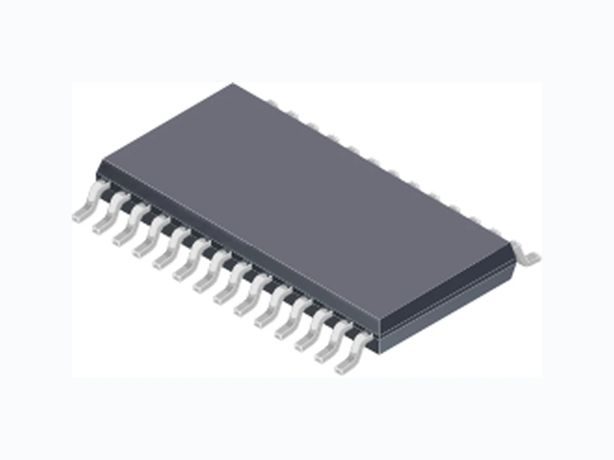
The A3944 is a programmable 6 channel low-side MOSFET pre-driver suitable for use in automotive applications. Each channel is controllable by a combination of parallel and serial inputs and provides sufficient gate drive current to allow PWM control up to 10 kHz, depending on the MOSFET gate charge. Each channel provides independent fault diagnostics for short to ground and open load when in the off-state, and short to battery when in the on-state. A short to battery can disable the output until reset or for a programmable retry time. Each channel provides independently programmable fault thresholds and blanking times. In addition to channel state control, channel fault masking, fault thresholds and fault timers are programmed through the SPI compatible serial interface. The serial interface also provides read back of the fault status for each channel. Digital inputs and outputs are compatible with 3.3 V and 5 V supplies. The A3944 is supplied in a 28 lead TSSOP package (suffix LP) with an exposed thermal pad. The package is lead (Pb) free with 100% matte-tin leadframe plating. A3944-DS, Rev. 1 Features and Benefits
- 6 channels
- Drives logic-level N-channel MOSFETs
- 50 mA gate drive current
- Short and open detection
- High voltage (50 V) drain feedback inputs
- Programmable fault timers and thresholds per channel
- UVLO and thermal warning circuitry
- Serial or parallel gate drive control
- Highly configurable, through SPI compatible interface
- Compact TSSOP package Automotive, Low-Side FET Pre-Driver Package: 28-pin TSSOP with exposed thermal pad (suffix LP) Typical Application Diagram Not to scale A3944 Applications:
- Automotive ECU
- Automotive high-side actuators Parallel SPI Controller A3944
Automotive, Low Side FET Pre-DriverA3944 2Allegro MicroSystems, Inc.
115 Northeast Cutoff
Worcester, Massachusetts 01615-0036 U.S.A. Selection Guide Part Number Packing* A3944KLPTR-T 4000 pieces per reel *Contact Allegro® for additional packing options Thermal Characteristics may require derating at maximum conditions, see application information Characteristic Symbol Test Conditions* Value Unit Package Thermal Resistance, Junction to Ambient RθJA 4-layer PCB based on JEDEC standard 28 ºC/W 2-layer PCB with 3.8 in.2 of copper area each side 32 ºC/W Package Thermal Resistance, Junction to Pad RθJP 2 ºC/W *Additional thermal information available on the Allegro website Absolute Maximum Ratings with respect to ground at TA = 25°C Characteristic Symbol Notes Rating Unit Analog Supply Voltage V BB –0.3 to 40 V Logic Supply Voltage V DD –0.3 to 6.5 V Gate Drive Supply Voltage V DR –0.3 to 6.5 V Terminal VREG V REG –0.3 to 20 V Terminals GATx –0.3 to 6.5 V Terminals DRNx –0.3 to 50 V Terminals INx –0.3 to 6.5 V Terminals SI, SCK, CSN –0.3 to 6.5 V Terminal SO –0.3 to 6.5 V Terminal RESETN –0.3 to 6.5 V Drain Feedback Clamp Energy* EDRNC Single pulse less than 2 ms 10 μJ Drain Feedback Clamp Current* IDRNC Single pulse not exceeding EDRN or PDRN 100 mA Drain Feedback Clamp Power* PDRNC Average power over any 2 ms period 100 mW Junction Temperature T J(max) 150 °C Transient Junction Temperature* TtJ Overtemperature event not exceeding 10 s, lifetime duration not exceeding 10 hours 175 °C Storage Temperature Range T stg –55 to 150 °C Operating Temperature Range T A Range K –40 to 150 °C *Guaranteed by design characterization.
Automotive, Low Side FET Pre-DriverA3944 3Allegro MicroSystems, Inc. Worcester, Massachusetts 01615-0036 U.S.A. Pin-out Diagram Terminal List Table Name Number Function Name Number Function CSN 23 Serial interface chip select IN1 21 Gate drive 1 control input DRN0 3 Gate drive 0 drain sense input IN2 20 Gate drive 2 control input DRN1 5 Gate drive 1 drain sense input IN3 19 Gate drive 3 control input DRN2 7 Gate drive 2 drain sense input IN4 18 Gate drive 4 control input DRN3 9 Gate drive 3 drain sense input IN5 17 Gate drive 5 control input DRN4 11 Gate drive 4 drain sense input PAD – Exposed thermal pad, connect to ground DRN5 13 Gate drive 5 drain sense input RESETN 27 Chip reset input GAT0 2 Gate drive 0 output SCK 25 Serial clock GAT1 4 Gate drive 1 output SI 24 Serial data input GAT2 6 Gate drive 2 output SO 26 Serial data output GAT3 8 Gate drive 3 output VBB 15 Analog supply (Battery) GAT4 10 Gate drive 4 output VDD 28 Logic Supply GAT5 12 Gate drive 5 output VDR 1 Gate drive supply GND 16 Power ground VREG 14 Voltage regulator IN0 22 Gate drive 0 control input VDR GAT0 DRN0 GAT1 DRN1 GAT2 DRN2 GAT3 DRN3 GAT4 DRN4 GAT5 DRN5 VREG VDD RESETN SO SCK SI CSN IN0 IN1 IN2 IN3 IN4 IN5 GND VBB PAD
Automotive, Low Side FET Pre-DriverA3944 4Allegro MicroSystems, Inc. Worcester, Massachusetts 01615-0036 U.S.A. Functional Block Diagram SPI Fault Logic Control Registers DRN0 GAT0 Gate Drive Channel DRN1 GAT1 DRN2 GAT2 DRN3 GAT3 DRN5 GAT5 Fault Register CSN SO SI SCK Retry Timer POR UVLO IN3 IN2 IN1 IN0 Clock RESETN VDD VDR GND VBB Config Register DRN4 GAT4 IN4IN5 GND GND Gate Drive Channel Config Register Gate Drive Channel Config Register Gate Drive Channel Config Register Gate Drive Channel Config Register Gate Drive Channel Config Register VDD VREG Regulator
Worcester, Massachusetts 01615-0036 U.S.A. Figure 1. Gate Drive Channel functional block diagram (shows 1 channel of 6)
Automotive, Low Side FET Pre-DriverA3944 6Allegro MicroSystems, Inc. Worcester, Massachusetts 01615-0036 U.S.A. ELECTRICAL CHARACTERISTICS Valid at TJ = –40°C to 150°C, VDD = 3.3 V, VDR = 5 V, VBB = 6 to 40 V; unless otherwise specified Characteristics Symbol Test Conditions Min. Typ. Max. Unit Supply and Reference Logic Supply Voltage V DD 3.0 – 5.5 V Analog Supply Voltage V BB 6 – 40 V Gate Drive Supply Voltage V DR 3.0 – 6.0 V VDD Quiescent Current I DDQ ––3 m A VBB Quiescent Current I BBQ ––4 m A VDD = 0, VBB ≤ 30 V – – 10 μA VDR Quiescent current I DRQ ––4 m A Regulator Voltage V REG VBB > 19.5 V 17.5 – 18.5 V Regulator Dropout V DO 0 – 0.6 V RESETN Pulse Width t RST 1–– μs RESETN Glitch Filter t RGF – – 200 ns Oscillator Frequency f OSC 1.4 2 2.6 MHz Digital Inputs and Outputs Input High Voltage V IH 70 – – %V DD Input Low Voltage V IL – – 30 %V DD Input Hysteresis V Ihys 300 500 – mV Input Pull-Up Resistor R PU CSN to VDD – 50 – k Ω Input Pull-Down Resistor R PD INx, SI, SCK to GND – 50 – k Ω SO Output High Voltage* V OH SO, IOH = –2 mA V DD - 0.4 V DD - 0.2 – V SO Output Low Voltage V OL SO, IOL = 2 mA – 0.2 0.4 V SO Output Leakage* I L CSN = VDD –1 – 1 μA Gate Output Drive Pull-Up On-Resistance* R DS(on)UP TJ = 25°C, IGHx = –20 mA 25 50 70 Ω TJ = 150°C, IGHx = –20 mA 50 75 125 Ω Pull-Down On-Resistance R DS(on)DN TJ = 25°C, IGLx = 20 mA 25 50 70 Ω TJ = 150°C, IGLx = 20 mA 50 75 125 Ω Output Sink Current I GL GATx off, VGATx = VDR 20 – – mA Output Source Current* I GH GATx on, VGATx = 0 V – – –50 mA Output Rise Time t r CLOAD = 400 pF, 20% to 80% VDR – 180 – ns Output Fall Time t f CLOAD = 400 pF, 80% to 20% VDR – 180 – ns Minimum On-Time t on At INx input – – 1 μs Minimum Off-Time t off At INx input – – 1 μs Turn-On Propagation Delay t P(on) INx to GATx – 200 – ns Turn-Off Propagation Delay t P(off) INx to GATx – 200 – ns RESETN to GATx – 0.5 1 μs Continued on the next page…
Automotive, Low Side FET Pre-DriverA3944 7Allegro MicroSystems, Inc. Worcester, Massachusetts 01615-0036 U.S.A. Fault Detection (On-State) Drain Clamp Voltage V DCL IDRNx = 10 μA4 5 – – V IDRNx = 10 mA – 54 – V Drain Clamp Leakage I DC VDRNx < 32 V – – 1 μA Short to Battery Threshold V STB GATx driven high, SB[2:0] = 111 30 31 32 %V REG GATx driven high, SB[2:0] = 110 17 18 19 %V REG GATx driven high, SB[2:0] = 101 15 16 17 %V REG GATx driven high, SB[2:0] = 100 13 14 15 %V REG GATx driven high, SB[2:0] = 011 11 12 13 %V REG GATx driven high, SB[2:0] = 010 9 10 11 %V REG GATx driven high, SB[2:0] = 001 7 8 9 %V REG GATx driven high, SB[2:0] = 000 5 6 7 %V REG Retry Timer t RE RT0 = 1 40 55 72 ms RT0 = 0 7 10 13 ms Fault Filter Time t FF(on) 1.25 2 2.75 μs Fault Blank Timer t BL(on) GATx driven high, TON[1:0] = 11 40 56 72 μs GATx driven high, TON[1:0] = 10 20 28 36 μs GATx driven high, TON[1:0] = 01 10 14 18 μs GATx driven high, TON[1:0] = 00 4 5 7 μs Fault Detection (Off-State) DRNx Pull-Up Diagnostic Current* I DPU GATx low, VDRNx < (VOCL – 200 mV) –80 –65 –50 μA DRNx Pull-Down Diagnostic Current I DPD GATx low, NPD = 0, VDRNx >(VOCL + 200 mV) 50 65 80 μA Short to Ground Threshold V STG GATx driven low, SG = 1 65 66 67 %V REG GATx driven low, SG = 0 44 45 46 %V REG Open Load Threshold V OL GATx driven low 75 76 77 %V REG Open Load Clamp Voltage V OCL 70 71 72 %V REG Fault Filter Time t FF(off) 1.25 2 2.75 μs Fault Blank Timer t BL(off) GATx driven low, TOF[1:0] = 11 3000 4000 5000 μs GATx driven low, TOF[1:0] = 10 200 280 360 μs GATx driven low, TOF[1:0] = 01 100 140 180 μs GATx driven low, TOF[1:0] = 00 60 80 100 μs ELECTRICAL CHARACTERISTICS (continued) Valid at TJ = –40°C to 150°C, VDD = 3.3 V, VDR = 5 V, VBB = 6 to 40 V; unless otherwise specified Characteristics Symbol Test Conditions Min. Typ. Max. Unit Continued on the next page…
Worcester, Massachusetts 01615-0036 U.S.A. *For input and output current specifications, negative current is defined as coming out of (sourcing) the specified device terminal. Figure 2. Serial Interface Timing Diagram. Letter keys refer to the Serial Interface Timing section of the Electrical
Automotive, Low Side FET Pre-DriverA3944 9Allegro MicroSystems, Inc. Worcester, Massachusetts 01615-0036 U.S.A. Functional Description The A3944 provides a programmable interface between an ECU and 6 low-side MOSFET switches in automotive applications. Each channel provides all the features necessary to drive and monitor the external FET and load. The gate of the external FET is driven by a 50 Ω (typ) push-pull driver capable of sourcing and sinking at least 50 mA under all conditions. This is sufficient to allow most typically used FETs to be switched with a PWM input at up to 10 kHz. The state of each channel is determined by a combination of parallel and serial inputs. When the FET is active its drain is monitored for a short to battery. When the FET is inactive, internal current sources are activated and the drain voltage is monitored to check for shorts to ground or open loads. The serial, SPI compatible interface provides access to control and configuration registers. Each channel has a dedicated fault configuration register that allows independent fault thresholds, fault timing, and fault configuration for each channel. The output state of each channel is determined by the logic con- trol input for the channel and a dedicated bit in the single output control register. Channels can therefore be controlled by parallel input, by serial input, or by a combination of the two. All chan- nels can be switched at the same time with a single serial write. A single fault mask register can be used to ignore the fault detect output for any channel combination. The serial interface also provides read back of the fault status for each channel. Digital inputs and outputs are compatible with 3.3 V and 5 V supplies. Terminal Functions VDD: Positive supply for digital input, output, and logic. VBB: Positive supply for voltage regulator. Can be connected to battery voltage through reverse polarity protection. VREG: Regulated voltage for analog and reference functions. VDR: Positive supply for gate drive outputs. GND: Ground return. Connect to common return point for all external MOSFET source connections. RESETN: Active low digital input. When held low for longer than the minimum reset pulse width: forces outputs low, resets the configuration, sets the LR bit, and resets all other channel faults. SI: Active high digital input with pull-down resistor. Data on SI is clocked into the serial register on the rising edge of SCK. SO: Push-pull digital output. Data from the fault register is output on SO, changing on the falling edge of SCK. SCK: Digital clock input with pull-down resistor. See SI and SO for action. CSN: Active low digital input with pull-up resistor. When CSN is low SO becomes active and data is accepted on SI. Data is latched in the serial register when CSN goes high. When CSN is high SO is high impedance and SI and SCK are ignored. INx: Active high digital inputs with pull-down resistors. When INx is high GATx is allowed to go high, depending the contents of the serial control register and any active faults. When INx is low GATx is held off. GATx: Gate drive outputs. Drive between GND and VDR. Con- nected through a resistor or directly to the gate of the external MOSFETs. DRNx: Analog, high-voltage inputs. Drain monitor connection used to determine the status of the drive to the load. Gate Drive Channels Each gate drive channel has independent control logic, gate drive output, fault detection circuitry, fault threshold generators, fault timers, and fault configuration register. The fault configuration register and reference generation provides two short to ground thresholds and eight short to battery thresholds, plus four turn-on blank times and four turn-off blank times independently select- able per channel. The gate drive channel block diagram (figure 1) shows the func- tional circuit for one gate drive channel, which is duplicated in each gate drive channel. A retry timer, common to all channels, allows automatic retry for short to battery faults. Control and Enable A gate drive output, GATx, is turned-on when: RESETN is high, no short to battery fault is present, and either the direct digital input, INx, or the relevant bit in the serial control register, Gx, is
Automotive, Low Side FET Pre-DriverA3944 10Allegro MicroSystems, Inc. Worcester, Massachusetts 01615-0036 U.S.A. high, in other words the logical OR of the INx input and the Gx bit for each channel x. If the GATx output is to be controlled by the serial interface, then the corresponding INx logic input should be held low. Internal pull-down resistors from each INx terminal to GND ensure that any unconnected input will be pulled low. Conversely, if the GATx output is to be controlled by the INx logic input, then the corresponding Gx bit in the control register should be set to 0, which is its default power-on and reset state. Gate Drive Output Each gate drive output is designed to provide symmetrical charge current from the VDR supply terminal and discharge current to the GND return terminal. The maximum source and sink imped- ance provides peak charge and discharge currents of at least 50 mA when connected directly to the gate of the external FET. This current can be limited, in order to limit the FET turn-on switching speed, by using a resistor between the GATx output and the gate of the FET. Although the GATx drive is designed to be symmetrical, the actual drive performance will be affected by the FET parameters and the resistance between the GATx output and the gate of the FET. The VDR supply is used only to supply the GATx output. The voltage at VDR can therefore be varied to provide voltage limited drive to the FET gate. Undervoltage detection is not provided for this supply. Reset Function If RESETN is held low for more than the minimum reset pulse width, then all registers are reset to their power-on state, and all GATx outputs are held low. Any latched channel faults and cor- responding bits in the fault register are reset, the logic reset (LR) bit is set, and the UV and OT bits reflect the status of the under- voltage and overtemperature detectors. The RESETN input uses a glitch filter to reduce the susceptibility to transients and noise on the RESETN input. This glitch filter is guaranteed to ignore any pulses shorter than the minimum RESETN glitch filter time, t RGF . Channel Fault Diagnostics All channel faults are determined by monitoring the voltage at the drain of the external FET through the DRNx terminal. Each chan- nel has independent bias current generators, programmable fault comparators, fault decode logic, and programmable fault timers. The serial interface provides a dedicated fault configuration reg- ister for each channel to select these features and thresholds per channel. A single fault mask register provides a fault mask bit for each channel. Fault detection is disabled when RESETN is low or when the fault mask bit is set. Fault reporting through the serial interface is fully described in the Serial Interface section below. A short to battery (short across the load to the load supply) can be detected when the channel is active, GATx is high, and the FET is on (on-state). A short to battery fault always attempts to protect the FET by pulling GATx low. A short to ground or open load can be detected when GATx is low and the FET is off (off-state). A short to ground fault or open load fault does not interfere with the operation of the GATx output. Each channel fault detected is latched as a fault state, and remains latched until the diagnostic circuits can determine that the fault has been removed for that channel. This determination can only occur at the end of a fault blank time. For short to battery this is at the end of the on-state fault blank time following a transition from off to on. For a short to ground or open load this is at the end of the off-state fault blank time following a transition from on to off. When a fault is detected, a dedicated bit in one of the two fault registers is set for each fault on each channel. This requires 3 bits per channel over 6 channels or 18 fault bits in total. The fault bits in the fault registers remain latched until the first serial transfer after the associated fault state has been reset. All latched fault states and all latched channel fault bits can also be cleared either by a power-on reset or by taking the RESETN terminal low. Practical limits for load resistance, and voltage conditions to provide effective determination of the load status, are discussed in the Applications Information section below. Note that each DRNx terminal has an internal Zener clamp which limits the voltage at the terminal to V DCL . If the voltage at the drain of the FET is likely to be higher than VDCL , even dur- ing a transient, then a current limit resistor, RDx , must be added
11Allegro MicroSystems, Inc. Worcester, Massachusetts 01615-0036 U.S.A. between the drain connection to the FET and the DRNx terminal. FET also would be detected as a short to battery. fault configuration register for the channel). fault filter is only active after the fault blank time. on, then it must be present for at least tFF(on) before it is detected. the channel from the control logic. Figure 3. Diagnostic Threshold Voltages
Automotive, Low Side FET Pre-DriverA3944 12Allegro MicroSystems, Inc. Worcester, Massachusetts 01615-0036 U.S.A. terminal. The voltage output capability of the current sources is limited such that they cannot source current when the output volt- age is greater than V OCL or sink current when the output voltage is less than VOCL. The equivalent circuit is shown in figure 4a. The typical sink and source currents are shown graphically in figure 4b. When a channel is in the off-state the current generators source or sink current through the DRNx terminal in an attempt to pull the voltage at the terminal to the open load clamp voltage, V OCL . The resulting voltage at the DRNx terminal, VDRNx , is measured to test for a short to ground or an open load. Normal Operation If a load is present, the load supply is active, and there are no shorts to ground, then the load will pull V DRNx above VOCL . VDRNx will then be greater than the open load threshold, VOL , and no fault is detected (see figure 3). If the NPD bit is zero then the current sink will pull IDPD from the supply through the load, through the DRNx terminal, to VOCL The open load threshold, VOL , and the open load clamp voltage, VOCL , are a both a fixed percentage of the voltage at the VREG terminal and are common to all channels. Short to Ground If a short to ground is present, then VDRNx will be pulled low by the short circuit. VDRNx will be less than the short detect thresh- old, VSTG , and a short to ground fault is reported (see figure 3). The short detect threshold voltage, VSTG , is selected, per channel, as a percentage of the voltage at the VREG terminal. The voltage selection is determined by the SG bit (bit 0 of the fault configura- tion register for the channel). Open Load If there is no short to ground or to supply, and the load is not con- nected, then the current sources will pull V DRNx towards the open load clamp voltage, VOCL . VDRNx will then be greater than VSTG but less than VOL and an open load is reported (see figure 3). The time taken for VDRNx to reach the correct value for an open fault condition depends on the current sourced from the DRNx terminal and on the capacitance connected to the drain of the FET. To avoid false fault detection at switch-off, the outputs from the short to ground and open load comparators are ignored during the off-state fault blank time, t BL(off) , after the GATx out- put drives low. One of four possible off-state fault blank times is selected, per channel, through the TOF0 and TOF1 bits (bits 6 and 7 of the fault configuration register for the channel). To avoid false fault detection during supply transients, an addi- tional fault filter masks faults that are present for less than the off-state fault filter time, t FF(off) . This fault filter is only active after the fault blank time. The result is that directly after switch-off, a short to ground or open load fault will not be detected until tBL(off) after the GATx output is commanded to drive low. If a fault occurs after tBL(off) from switch-off then it must be present for at least tFF(off) before it is detected. In some applications, for example when driving high efficiency LEDs, the load may be sensitive to the pull down current used to VDRNx DRNx VOCL GND IDPD IDPU IDRNx 100 –20 –40 –60 –80 –100 02468 1 0 IDRNx (μA) VDRNx (V) VOCL IDPD NPD = 0 NPD = 1 IDPU Figure 4a. Diagnostic Current Source Circuit Figure 4b. Diagnostic Currents
Automotive, Low Side FET Pre-DriverA3944 13Allegro MicroSystems, Inc. Worcester, Massachusetts 01615-0036 U.S.A. ensure open load detection. In these cases this pull-down current can be disabled by setting the NPD bit (bit 8 in the fault con- figuration register for the channel). If the NPD bit is set then it is possible that V DRNx will reach the correct value for an open fault condition when the load is connected, resulting in a false open load detection. If this is likely, there are two options:
- Set the fault mask bit for the channel. This will mask all faults on that channel and may not be a suitable option.
- Set the open load fault mask bit, OLM (bit 6 in the fault mask register). This will disable open load detection on any channel where NPD is set to 1. Chip Diagnostics The chip temperature and the supply voltage levels at VDD and VREG are monitored to ensure correct and safe operation of the circuit. VDD is monitored to ensure that power-up and power-down does not cause incorrect operation. All outputs will be switched to high impedance, the VREG regulator will be disabled and all faults reset when the voltage at VDD, V DD , falls below the undervolt- age level, VDDUV . The outputs will be reactivated when VDD rises above the undervoltage turn-on level plus the hysteresis voltage, defined as V DDUV + VDDUVhys . When VDD rises above this threshold, all registers will be reset to their power-on state, and all GATx outputs will be low. In the fault register any latched channel faults will be reset, the logic reset (LR) and undervoltage (UV) bits will be set, and the OT bit will reflect the status of the overtemperature monitor. VREG is monitored to ensure correct operation of the fault detection and control circuits. All channel faults will be reset when the voltage at VREG, V REG , falls below the undervoltage level, VREGUV . They will be held reset until VREG rises above the undervoltage lockout level plus the hysteresis voltage, VREGUV + VREGUVhys . The outputs will remain active irrespective of the value of VREG . The chip temperature is monitored by the thermal warning cir- cuit. An overtemperature fault will be indicated but no action will be taken when the chip temperature exceeds the overtemperature warning level TJW . It is incumbent upon the user to take any nec- essary action to limit dissipation to reduce the temperature. Serial Interface The inputs CSN, SCK, and SI provide a three wire synchronous serial interface, compatible with SPI, that can be used to control all features of the A3944. The output, SO, can be used to provide a fourth interface connection for detailed diagnostic feedback. The serial interface timing requirements are specified in the Elec- trical Characteristics table, and illustrated in the Serial Interface Timing diagram, figure 2. Data is received on the SI terminal and clocked through a shift register on the rising edge of the clock signal input on the SCK terminal. CSN is normally held high, and is only brought low to initiate a serial transfer. No data is clocked through the shift register when CSN is high, allowing multiple slave units to use common SI, SCK, and SO connections. Each slave then requires an independent CSN connection. When 16 data bits have been clocked into the shift register, CSN must be taken high to latch the data into the selected register. When this occurs, the internal control circuits act on the new data and the fault register is reset. If there is either: more than 16 rising edges on SCK, or at least one but fewer than 16 rising edges on SCK and CSN goes high, then the write will be cancelled without writing data to the regis- ters or resetting the diagnostic registers. The FF bit will be set to indicate a data transfer error. Configuration and Control Registers The serial data word is 16 bits, input MSB first. The first four bits are defined as the register address. This provides sixteen write- able registers: Address 1: Gate Select Register The six least significant bits of this register are the control bits for each of the six channels. G0 corresponds to channel 0, G1 to channel 1, and so forth. If RESETN is high and no faults are pres- ent on the channel, then when the Gx bit for a channel is set to 1 the GATx output will be high.
Automotive, Low Side FET Pre-DriverA3944 14Allegro MicroSystems, Inc. Worcester, Massachusetts 01615-0036 U.S.A. Address 5: Fault Mask Register The six least significant bits of this register are the fault mask bits for each of the six channels. K0 corresponds to channel 0, K1 to channel 1, and so forth. When the K bit for a channel is set to 1 all faults on that channel are ignored and no faults are reported for that channel. Bit 6 is an open load fault mask bit, OLM, that disables the open load detection on any channel where NPD is set to 1. Addresses 8 to 13: Channel Fault Configuration Registers These six registers, one per channel, determine the fault threshold levels, fault blank times, and fault features for each channel. The MSB is always set to 1. The next three bits, bits 12,13, and 14, are the channel address bits. The remaining register addresses are unused. Writing to these addresses will have no effect on the operation but will still report the fault register on SO. Fault Register In addition to the writable registers there are two fault registers, Fault0 and Fault1. The register being output is identified by bit 11, which contains a zero for Fault0 and a one for Fault1. Each time any register is written through the serial interface, one of the fault registers can be read, MSB first, on the serial output terminal, SO (see the Serial Interface Timing diagram, figure 2). Fault0 is output: on the first write after a power-on-reset, after a RESETN low input, or after a serial fault poll (described in the next paragraph). Fault1 is then read on the next write. The two registers then alternate on each successful serial write sequence. The first, most significant, bit in both fault registers is the fault register flag, FF (bit 15). This bit is set to one, if any faults have been detected since the last fault reset. The state of FF appears on SDO as soon as CSN goes low, allowing the fault status to be determined without a change in the level of SCK. A serial trans- fer may be terminated when CSN goes low then high, without generating a serial read fault, by ensuring that SCK remains high while CSN is low. This allows the main controller to poll the A3944 through the serial interface to determine if a fault has been detected. When this occurs the fault register pointer is reset to the Fault0 register, so the next full write sequence outputs the Fault0 register. The fault status can also be read, without disturbing any settings, by writing to one of the unused register addresses. In this case the fault registers will continue to alternate between Fault0 and Fault1. The next three most significant bits, after FF, in each fault regis- ter are the system diagnostic bits: UV (bit 14), LR (bit 13), and OT (bit 12). These provide an indication of undervoltage, logic reset, and overtemperature faults. Bit 11 (FR) indicates which of the two fault registers is being output on SO. This bit is a zero for the Fault0 register and a one for the Fault1 register. The least significant 9 bits in each fault register provide three bits per channel, one bit for each of the three possible fault states: short to battery, short to ground, and open load. Fault0 con- tains the fault data for channels 0, 1, and 2. Fault1 contains the fault data for channels 3, 4, and 5. The bits naming convention indicates the channel and fault allocation. The format is “ccff,” where “cc” is C0, C1, C2, C3, C4, or C5 (indicating the channel) and “ff” is SG, SB, or OL (indicating the faults: short-to-ground, short-to-battery and open-load respectively). The contents of the fault register that is being read cannot change when CSN is low and a serial read is in progress. Any faults detected during a serial read do affect the read in progress but the fault will be latched in the fault register when CSN goes high at the end of a serial read. The fault bits can only be cleared after: either the diagnostic circuits have confirmed that the fault that has been reported is no longer present, or there is a low level on the RESETN input. In the case of undervoltage or overtemperature faults, which are not latched, the fault bits will be reset at the end of a serial read if the fault is not detected at that time. For channel faults, which are latched, the fault bits will be reset at the end of a serial read if the diagnostic circuits have previously determined that the fault that has been reported is no longer pres- ent. This determination can only occur at the end of a fault blank time and therefore requires: either an on-to-off transition (for short to ground and open load faults), or an off-to-on transition (for short to battery faults) on the faulty channel before the start of a serial read. Any changes to the fault state when a read is in progress are ignored until the end of the serial read. If a fault is cleared when a serial read is in progress, then the fault bits will be cleared when CSN goes high.
15Allegro MicroSystems, Inc. Worcester, Massachusetts 01615-0036 U.S.A. the relative voltage, DRNx, at the drain of the external MOSFET. and the resulting data bits read for the channel. Figure 5. Fault Sequence: Short to battery during off-state (RT1=1) Figure 6. Fault Sequence: Short to ground during on-state
16Allegro MicroSystems, Inc. Worcester, Massachusetts 01615-0036 U.S.A. Figure 7. Fault Sequence: Open load during on-state Figure 8. Fault Sequence : Short to battery during on-state (RT1=1)
17Allegro MicroSystems, Inc. Worcester, Massachusetts 01615-0036 U.S.A. Figure 9. Fault Sequence: Short to ground during off-state Figure 10. Fault Sequence: Short to battery during on-state followed immediately by open load (RT1=0)
18Allegro MicroSystems, Inc. Worcester, Massachusetts 01615-0036 U.S.A. Figure 11. Power Sequence Timing- VDD before VBB Figure 12. Power Sequence Timing- VDD after VBB - with RESET
Automotive, Low Side FET Pre-DriverA3944 19Allegro MicroSystems, Inc. Worcester, Massachusetts 01615-0036 U.S.A. Gate Select Register G[5..0] Control bits for each of the six channels. G0 corresponds to channel 0, G1 to channel 1 etc. If RESETN is high and no faults are present on the channel then when the Gx bit for a channel is set to 1 the GATx output will be high Fault Mask Register K[5..0] Fault mask bits for each of the six channels. K0 corresponds to channel 0, K1 to channel 1 etc. When the Kx bit for a channel is set to 1 all faults on that channel are ignored and no faults are reported for that channel. OLM Open load fault mask for all channels where NPD=1. If the NPD bit is set to 1 on a channel and OLM is set to 1 then the open load diagnostic is disabled for that channel. Fault0/Fault1 Registers FF Logic 1 if any faults have been detected since the last fault reset. UV Logic 1 if any VDD or VREG undervoltage faults have been detected since the last fault reset. LR Logic 1 if a logic reset has occurred since the last register read. A logic reset is caused by a power- on-reset or by taking the RESETN input low. OT Logic 1 if an overtemperature fault has been detected since the last fault reset. FR Fault register identifier. Logic 0 for Fault0 register, logic 1 for Fault1 register. CxSG Logic 1 if channel short to ground detected. Where x is channel number. CxSB Logic 1 if channel short to battery detected. Where x is channel number. CxOL Logic 1 if channel open load detected. Where x is channel number. Serial Register Definition* 0 1 2 3 4 5 6 7 8 9 01 11 21 31 41 51 Gate Select 0 0 0 1 G5 G4 G3 G2 G1 G0 0 0 0 0 0 0 0 0 0 0 0 0 Fault Mask 0 1 0 1 OLM K5 K4 K3 K2 K1 K0 0 0 0 0 0 0 0 0 0 0 0 0 Channel Fault Config 1 ADR2 ADR1 ADR0 RT1 RT0 NPD TOF1 TOF0 TON1 TON0 SB2 SB1 SB0 SG 0 0 0 0 0 0 0 0 0 0 0 0 Fault0 FF UV LR OT FR 0 0 C2SG C2SB C2OL C1SG C1SB C1OL C0SG C0SB C0OL
1 UV 1 OT 0 0 0 0 0 0 0 0 0 0 0 0
FF UV LR OT FR 0 0 C5SG C5SB C5OL C4SG C4SB C4OL C3SG C3SB C3OL
1 UV 1 OT 1 0 0 0 0 0 0 0 0 0 0 0
*Power on reset value shown below each input register bit.
Automotive, Low Side FET Pre-DriverA3944 20Allegro MicroSystems, Inc. Worcester, Massachusetts 01615-0036 U.S.A. Channel Fault Config Register ADDR[2..0] Channel address ADR2 ADR1 ADR0 Address 0 0 0 Channel 0 0 0 1 Channel 1 0 1 0 Channel 2 0 1 1 Channel 3 1 0 0 Channel 4 1 0 1 Channel 5 RT[1..0] Retry select RT1 RT0 Fault
0 X Lockout until reset
1 0 Short retry timer. Nominally 10ms 1 1 Long retry timer. Nominally 55ms NPD Disable diagnostic pull-down NPD Action
0 Enable diagnostic pull-down
1 Disable diagnostic pull-down
TOF[1..0] Turn-off blank time select. TOF1 TOF0 Turn-off blank time (nominal) 0 0 80 μs 0 1 140 μs 1 0 280 μs 1 1 4ms TON[1..0] Turn-on blank time select. TON1 TON0 Turn-on blank time (nominal) 0 0 5 μs 0 1 14 μs 1 0 28 μs 1 1 56 μs SB[2..0] Short to battery threshold select SB2 SB1 SB0 Threshold (nominal) 0 0 0 6% V REG 0 0 1 8% V REG 0 1 0 10% V REG 0 1 1 12% V REG 1 0 0 14% V REG 1 0 1 16% V REG 1 1 0 18% V REG 1 1 1 31% V REG SG Short to ground threshold select. SG Threshold (nominal) 0 45% V REG 1 66% V REG For tolerances on selected parameters refer to the Electrical Characteristics Table. Serial Register Definition* 0 1 2 3 4 5 6 7 8 9 01 11 21 31 41 51 Channel Fault Config 1 ADR2 ADR1 ADR0 RT1 RT0 NPD TOF1 TOF0 TON1 TON0 SB2 SB1 SB0 SG 0 0 0 0 0 0 0 0 0 0 0 0 *Power on reset value shown below each input register bit.
Automotive, Low Side FET Pre-DriverA3944 21Allegro MicroSystems, Inc. Worcester, Massachusetts 01615-0036 U.S.A. Applications Information Drain Feedback Clamp Resistor Selection The drain feedback input, DRNx, for each channel is clamped internally with a 50 V (nominal) Zener diode. If the voltage applied to this terminal is likely to exceed 50 V then an external current limit resistor will be required to limit the current, power, and energy to less than the Absolute Maximum specifications in this document. Note that the internal drain clamp in the A3944 is not intended to dissipate the energy from any external load. The internal clamp is provided to protect the internal circuits of the A3944 from any high voltage that would otherwise cause permanent damage. If the voltage at DRNx, V DRNx , will never exceed the minimum drain clamp voltage, VDCL , then no external resistor is required and DRNx can be connected directly to the drain of the external MOSFET switch. Three Absolute Maximum specifications apply to the A3944, none of which may be exceeded:
- The maximum clamp current, I DRNC , applies to very short pulses, typically less than 1.85 μs. Any current pulse less than 1.85 μs and less than IDRNC , will never exceed the maximum power or energy limits.
- The maximum clamp energy, EDRNC , applies to pulses between 1.85 μs and 2 ms. Above 2 ms the heat produced by the clamp energy dissipates through the silicon and the package; in that case, the maximum clamp power applies. Note that for pulse lengths between about 500 μs and 2 ms the energy starts to dis- sipate during the pulse, so the maximum current that is possible will actually be higher than that calculated using the maximum energy limit.
- The maximum clamp power, P DRNC , applies to pulses lasting longer than 2 ms up to continuous operation. Maximum current example:
- Load resistance: 26 Ω
- Load inductance: 130 μH
- Load current: 0.5 A
- Load supply voltage: 13 V
- FET clamp voltage: 80 V These values would typically apply to a remote load which is primarily resistive. The load inductance will be due to a combina- tion of the wiring and any parasitic inductance in the load. In this example, the DC on-state current will be 13 V / 26 Ω = 0.5 A. When the load is switched off, the inductance attempts to keep the current flowing by increasing the voltage at the end connect to the FET switch. This voltage increases up to the breakdown voltage of the FET. At that point, the voltage across the load amounts to the difference between the FET breakdown voltage and the supply voltage, and it acts to reduce the current. With the parameters in this example, the current would decay to zero in less than 1 μs. This is less than the 1.85 μs limit for maximum current, so the drain resistor will be based only on the maximum current. The value of the drain resistor, R Dx , in this case is simply the voltage across the resistor divided by the maximum current: RDx = IDRNC VFET – VDCL (1) where VFET is the FET breakdown voltage, VDCL is the A3944 drain clamp voltage, and IDRNC is the A3944 drain clamp max current. Substituting into equation 1: RDx = = 260 Ω100 mA
80 V – 54 V
The energy injected into the A3944 drain clamp is: EDRNC = VDCL × IDRNC × tPULSE (2) where tPULSE is the duration of the current pulse. Substituting into equation 2: EDRNC = 54 V × 100 mA × 0.9 μs = 4.86 μJ (per pulse) As expected, based on the pulse length, this is less than half the clamp energy limit, given in the Absolute Maximum table.
Automotive, Low Side FET Pre-DriverA3944 22Allegro MicroSystems, Inc. Worcester, Massachusetts 01615-0036 U.S.A. The maximum repetition rate of this pulse is derived from the maximum average clamp power dissipation limit. The minimum time between pulses, t REP , is: tREP = EDRNC PDRNC (3) where PDRNC is the A3944 drain clamp maximum power. Substituting into equation 3: tREP == 48.6 μs4.86 μJ 100 mW resulting in a repetition rate of just over 20 kHz. Maximum energy example:
- Load resistance: 18 Ω
- Load inductance: 1 mH
- Load current: 0.72 A
- Load supply voltage: 13 V
- FET clamp voltage: 80 V These values would typically apply to a small inductive load such as a solenoid or relay. When the load is switched off, the inductance attempts to keep the current flowing by increasing the voltage at the end connected to the FET switch. This voltage increases up to the breakdown voltage of the FET. At that point, the voltage across the load amounts to the difference between the FET breakdown voltage and the supply voltage, and it acts to reduce the current. With the parameters in this example, the cur- rent would decay to zero in about 10 μs. This is greater than the 1.85 μs pulse time defining the maximum current but less than the 2 ms time constant for maximum average clamp power, so the drain resistor will be selected to limit the energy injected into the drain clamp in the A3944. The maximum current, the A3944 drain clamp maximum current, I DRNC , will be: IDRNC = EDRNC VDCL × tPULSE (4) where EDRNC is the A3944 drain clamp maximum energy, VDCL is the A3944 drain clamp voltage, and tPULSE is the duration of the current pulse. Substituting into equation 4: IDRNC == 18.5 mA10 μJ
54 V × 10 μs
As given in equation 1, the value of the drain resistor is the volt- age across the resistor divided by the maximum current: RDx = IDRNC VFET – VDCL RDx = = 1.4 kΩ18.5 mA As given in equation 3, the maximum repetition rate of this pulse is derived from the maximum average clamp power dissipation limit as: tREP = EDRNC PDRNC tREP == 100 μs10 μJ 100 mW resulting in a repetition rate of 10 kHz. Maximum power example:
- Load resistance: 5 Ω
- Load inductance: 80 mH
- Load current: 2.6 A
- Load supply voltage: 13 V
- FET clamp voltage: 60 V These values would typically apply to a large inductive load such as a coil or actuator. When the load is switched off, the inductance attempts to keep the current flowing by increasing the voltage at the end connected to the FET switch. This voltage increases up to the breakdown voltage of the FET. At that point, the voltage across the load amounts to the difference between the FET breakdown voltage and the supply voltage, and it acts to reduce the current. With the parameters in this example, the current would decay to zero in about 4 ms. This is greater than the 2 ms time constant for maximum average clamp power, so the drain resistor will be selected to limit the power dissipated by
23Allegro MicroSystems, Inc. Worcester, Massachusetts 01615-0036 U.S.A. VDCL is the A3944 drain clamp voltage.
60 V – 54 V
A3944 will sustain the maximum clamp dissipation indefinitely. RD is the DRNx current limit resistor. where VOCL is the open load clamp voltage. nostic currents, and the load voltage. Figure 13. Open load detection condition
24Allegro MicroSystems, Inc. Worcester, Massachusetts 01615-0036 U.S.A. than 12 kΩ will never cause an open load detection. not to be detected as an open load. zero resistance and the short would be to ground at zero volts. a short to ground is shown in figure 15. Figure 14. Open load detection limits Figure 15. Short to ground detection condition
25Allegro MicroSystems, Inc. Worcester, Massachusetts 01615-0036 U.S.A. RD is the DRNx current limit resistor. where VOCL is the open load clamp voltage. ing on the relative values of RDmax and VL . same conditions give 0.9 Ω for SG = 0 and 0.34 Ω for SG = 1. +1 V offset ground. An increase in RD raises the line. Figure 16. Short to ground detection limits
26Allegro MicroSystems, Inc. Worcester, Massachusetts 01615-0036 U.S.A. RSB is the resistance of the short across the load. under normal operating conditions. VREGmax + VDOmin ) and VSTB is at the maximum tolerance value. Figure 17. Short to battery detection condition
27Allegro MicroSystems, Inc. Worcester, Massachusetts 01615-0036 U.S.A. 100 mΩ MOSFET using short to battery threshold level 5. faster short to battery detection and a lower short circuit current. 100 mΩ MOSFET using short to battery threshold level 5. Figure 18. Short to battery detection limits
Automotive, Low Side FET Pre-DriverA3944 28Allegro MicroSystems, Inc. Worcester, Massachusetts 01615-0036 U.S.A. Quiescent Dissipation The quiescent dissipation for each supply is the simply product of the supply current and the supply voltage: P DD = VDD × IDDQ P BB = VBB × IBBQ P BR = VDR × IDRQ From the Electrical Characteristics table specification this gives the total maximum quiescent dissipation of 131 mW when VDD and VDR are 5 V and VBB is 24 V . At 12 V this drops to 83 mW. Channel Switching Dissipation The dissipation produced by switching each channel on or off is calculated by summing the energy passing through the gate drive output to and from the gate of the external MOSFET over time. The energy transferred to the gate is given by: 2ESW = Qg VG (23) where Qg is the total MOSFET gate charge and VG is the MOSFET gate voltage when on. This is the energy transferred through the gate drive each time a MOSFET is switched on or off. The total power due to this energy transfer is calculated by multiplying the energy by the number of switching events per second. The number of switching events per second is twice the PWM frequency, so the dissipation due to switching losses becomes: P SW = Qg VG fPWM (24) where fPWM is the PWM frequency for the channel. If there is no gate resistor then this is the total dissipation that will occur inside the A3944. If a gate resistor is used then the dissipa- tion will be shared proportionally by the gate resistor and by the on-resistance of the A3944 gate drive. This gives the equation for internal dissipation as: RON RON + RG PSW = Qg VG fPWM (25) where RON is the on-resistance of the gate drive and RG is the gate resistor value. As an example, the maximum likely switching losses can be estimated by using a reasonably large MOSFET total charge of 100 nC and a PWM frequency of 10 kHz. With no gate resistor the dissipation in the A3944 due to switching losses for a single channel will be approximately 5 mW. Channel Diagnostic Dissipation Each channel has three current generators that are used to deter- mine the state of the load during the off-state for the channel. Under normal load conditions the power dissipated is limited to the product of the pull-down current source and the difference between the load supply and the open load clamp voltage. For example, with a 24 V load supply, this would contribute a maxi- However, the worst case dissipation will occur when the load is not connected and a capacitor is attached to the diagnostic feedback terminal for the channel, DRNx. As for the switching losses, the dissipation can be calculated by summing the energy transferred to the capacitor over time. In this case the energy transferred is: 2ED = CD V 2OCL (26) where CD is the value of the DRNx capacitor and VOCL is the offset clamp voltage. This is the energy transferred through the current source each time a MOSFET is switched off. The total power due to this energy transfer is calculated by multiplying this energy by the number of switching events per second. The number of switching events per second is the PWM frequency, so the dissipation due to switching losses becomes: 2PD = CD V 2OCL fPWM (27) where fPWM is the PWM frequency for the channel. As an example, a 10 nF capacitor and a PWM frequency of 10 kHz will produce a dissipation in the A3944 for a single chan- nel of approximately 4.3 mW. This is the worst case dissipation. It will not be present if a load is attached and will be reduced by any DRNx current limit resistor.
29Allegro MicroSystems, Inc. Worcester, Massachusetts 01615-0036 U.S.A. no gate resistors, then the maximum dissipation will be 275 mW. ply and to 139 mW with a 12 V supply. ,and 114 mW at 12 V (see figure 19). Figure 19. Power dissipation all loads connected
Automotive, Low Side FET Pre-DriverA3944 30Allegro MicroSystems, Inc. Worcester, Massachusetts 01615-0036 U.S.A. Package LP, 28-Pin TSSOP with Exposed Thermal Pad A
1.20 MAX
0.15 0.00 0.30 0.19 0.20 0.09 0.60 ±0.15
1.00 REF
C SEATING PLANEC0.10 28X
0.65 BSC
0.25 BSC
9.70±0.10 GAUGE PLANE SEATING PLANE A Terminal #1 mark area B For Reference Only; not for tooling use (reference MO-153 AET) Dimensions in millimeters Dimensions exclusive of mold flash, gate burrs, and dambar protrusions Exact case and lead configuration at supplier discretion within limits shown B C Exposed thermal pad (bottom surface); dimensions may vary with device Branded Face 6.10 0.65 0.45 1.65 3.00 5.00 PCB Layout Reference ViewC
5.08 NOM
3 NOM
Reference land pattern layout (reference IPC7351 SOP65P640X120-29CM); All pads a minimum of 0.20 mm from all adjacent pads; adjust as necessary to meet application process requirements and PCB layout tolerances; when mounting on a multilayer PCB, thermal vias at the exposed thermal pad land can improve thermal dissipation (reference EIA/JEDEC Standard JESD51-5)
Automotive, Low Side FET Pre-DriverA3944 31Allegro MicroSystems, Inc. Worcester, Massachusetts 01615-0036 U.S.A.
Revision History
Revision Revision Date Description of Revision Rev. 1 May 18, 2012 Update R DS(on) , IBBQ , and IGL Copyright ©2011-2012, Allegro MicroSystems, Inc. Allegro MicroSystems, Inc. reserves the right to make, from time to time, such de par tures from the detail spec i fi ca tions as may be required to per- mit improvements in the per for mance, reliability, or manufacturability of its products. Before placing an order, the user is cautioned to verify that the information being relied upon is current. Allegro’s products are not to be used in life support devices or systems, if a failure of an Allegro product can reasonably be expected to cause the failure of that life support device or system, or to affect the safety or effectiveness of that device or system. The in for ma tion in clud ed herein is believed to be ac cu rate and reliable. How ev er, Allegro MicroSystems, Inc. assumes no re spon si bil i ty for its use; nor for any in fringe ment of patents or other rights of third parties which may result from its use. For the latest version of this document, visit our website: www.allegromicro.com