

 Download PDF
DATASHEET SEARCH SITE
Document overview
- PDF pages: 2
Technical content
Page 1
High Voltage MOSFET
N-Channel Enhancement Mode
Avalanche Energy Rated
Preliminary Data
Symbol
Test Conditions
TJ = 25°C to 150°C
VDSS
TJ = 25°C to 150°C; RGS = 1 MΩ
VDGR
Continuous
VGS
Transient
VGSM
TC = 25°C
ID25
TC = 25°C, pulse width limited by TJM
IDM
IXTA 1N80
= 800 V
VDSS
IXTP 1N80
ID25
= 750 mA
IXTY 1N80
= 11 ΩΩΩΩΩ
RDS(on)
Maximum Ratings
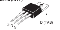
TO-220AB (IXTP)
800
V
800
V
±20
V
±30
V
750 mA
3 A
G S D (TAB)
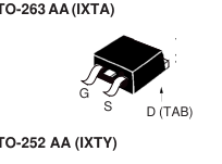
G = Gate,
D = Drain,
S = Source,
TAB = Drain
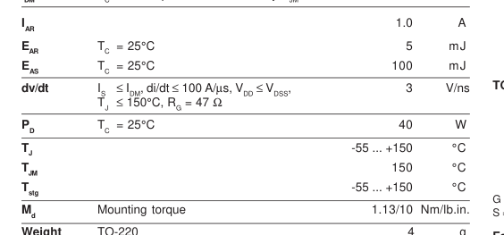
Weight
Features
TO-252 0.8
g
TO-263 3
Maximum lead temperature for soldering 1.6 mm (0.062 in.) from case for 10 s
Symbol
Test Conditions
g ! International standard packages °C ! High voltage, Low RDS (on) HDMOSTM 300
process
! Rugged polysilicon gate cell structure ! Fast switching times
Characteristic Values
(TJ = 25°C, unless otherwise specified)
Applications
| min. | typ. | max. |
|---|---|---|
| V V = 0 V, I = 250 µA 800 DSS GS D V V = V GS, I = 25 µA 2.5 GS(th) DS D | V 4.5 V | |
| I V = ±20 V DC, V = 0 GSS GS DS | ±100 nA | |
| I V = V T = 25°C DSS DS DSS J V = 0 V T = 125°C GS J | 25 µA 500 µA | |
| R V = 10 V, I = 500 mA DS(on) GS D Pulse test, t ≤ 300 µs, duty cycle d ≤ 2 % | 9.5 | 11 Ω |
! Switch-mode and resonant-mode
power supplies
! Flyback inverters ! DC choppers ! High frequency matching
Advantages
! Space savings ! High power density
DS98822C(11/03)
© 2003 IXYS All rights reserved
Page 2
IXTP 1N80 IXTA 1N80
IXTY 1N80
Characteristic Values
Symbol
Test Conditions
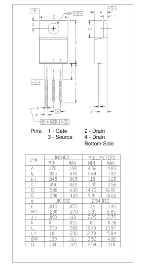
TO-220 AD Dimensions
(TJ = 25°C, unless otherwise specified)
min. typ.
max.
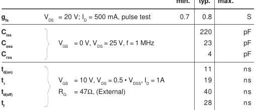
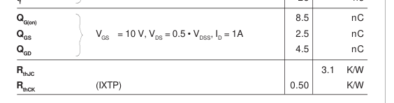
Characteristic Values
Source-Drain Diode
(TJ = 25°C, unless otherwise specified)
Symbol
Test Conditions
min. typ.
max.
VGS = 0 V
750 mA
IS
| I Repetitive; pulse width limited by T SM JM | 3 A | |
| V I = I , V = 0 V, SD F S GS Pulse test, t ≤ 300 µs, duty cycle d ≤ 2 % | 1.8 | 2 V |
| t I = I , -di/dt = 100 A/µs, V = 100 V rr F S R | 710 | ns |
TO-252 AA Outline
Dim. Millimeter
Inches Min. Max. Min. Max.
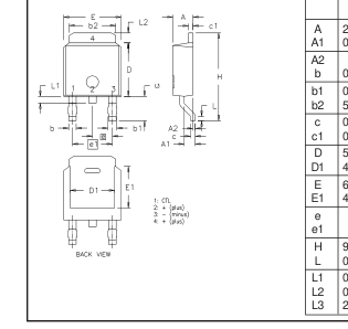
| A A1 A2 b | 2.19 2.38 0.89 1.14 0 0.13 0.64 0.89 | 0.086 0.094 0.035 0.045 0 0.005 0.025 0.035 |
| b1 b2 | 0.76 1.14 5.21 5.46 | 0.030 0.045 0.205 0.215 |
| c | 0.46 0.58 | 0.018 0.023 |
| c1 D D1 | 0.46 0.58 5.97 6.22 4.32 5.21 | 0.018 0.023 0.235 0.245 0.170 0.205 |
| E E1 | 6.35 6.73 4.32 5.21 | 0.250 0.265 0.170 0.205 |
| e e1 | 2.28 BSC 4.57 BSC | 0.090 BSC 0.180 BSC |
| H L | 9.40 10.42 0.51 1.02 | 0.370 0.410 0.020 0.040 |
| L1 L2 L3 | 0.64 1.02 0.89 1.27 2.54 2.92 | 0.025 0.040 0.035 0.050 0.100 0.115 |
IXYS reserves the right to change limits, test conditions, and dimensions. IXYS MOSFETs and IGBTs are covered by one or more of the following U.S. patents:
4,835,592 4,881,106 4,850,072 4,931,844
TO-263 AA Outline
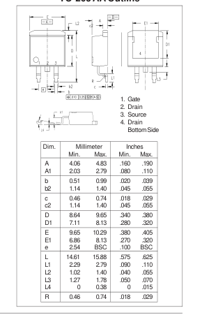
5,017,508 5,049,961 5,187,117 5,486,715 6,306,728B1
5,034,796 5,063,307 5,237,481 5,381,025