
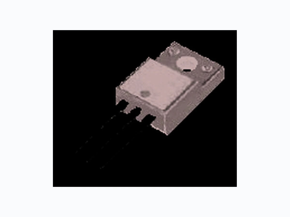
8N60 NELLSEMI
Document overview
- Manufacturer or author: Provided By www.digicamel.com(FREE DATASHEET DOWNLOAD SITE)
- PDF pages: 7
Technical content
(8A, 600Volts) They are designed for use in applications. such as switched mode power supplies, DC to DC converters, PWM motor controls, bridge circuits, and general purpose switching applications . The Nell 8N60 is a three-terminal silicon device with current conduction capability of 8A, fast switching speed, low on-state resistance, breakdown voltage rating of 600V ,and max. threshold voltage of 4 volts.
DESCRIPTION
Low reverse transfer capacitance (C = 12pF typical)RSS R = 1.2Ω @ V = 10V DS(ON) GS Ultra low gate charge(36nC max.) Fast switching capability 100% avalanche energy specified Improved dv/dt capability 150°C operation temperature
FEATURES
I (A)D 8 V (V)DSS 600 1.2 @ V = 10VGS R (Ω)DS(ON) Q (nC) max.G D (Drain) G (Gate) S (Source) 2TO-263(D PAK) (8N60H) UNIT V /ns V W A mJ ºC -55 to 150 VALUE 600 ±30 600 150 4.5 ABSOLUTE MAXIMUM RATINGS (T = 25°C unless otherwise specified)C T =25°C to 150°CJ TEST CONDITIONS R =20KΩGS T =25°C C T =100°C C Operation junction temperature Storage temperature Single pulse avalanche energy(Note 2) PARAMETER Pulsed Drain current(Note 1) Continuous Drain Current Peak diode recovery dv/dt(Note 3) Gate to Source voltage Drain to Gate voltage Drain to Source voltage SYMBOL VDGR VDSS dv/dt VGS IDM TSTG PD ID TJ TL . .lbf in (N m) 300Maximum soldering temperature, for 10 seconds Mounting torque, #6-32 or M3 screw -55 to 150 Note: 1. . Repetitive rating: pulse width limited by junction temperature. 10 (1.1) 1.6mm from case IAR Avalanche current(Note 1) 14.7 T =25°C C 2.I = 8A, V = 50V, L = 7.1mH, R = 25Ω, starting T =25°C.AS DD GS J 230 Repetitive avalanche energy(Note 1)EAR 3.I ≤ 7.5A, di/dt ≤ 200A/µs, V ≤ V , starting T =25°C.SD DD (BR)DSS J Total power dissipation G S D I =8A, R =50Ω, V =10V AR GS GS EAS I =8A, L=7.1mHAS www.nellsemi.com Page 1 of 7 TO-220AB (8 )N60A TO-220F (8 )N60AF D GDS G SD TO-220AB/TO-263 TO-220F
UNITMin. 0.85 2.6 THERMAL RESISTANCE PARAMETER Thermal resistance, junction to case SYMBOL Rth(j-c) Typ. Max. ºC/W 62.5Thermal resistance, junction to ambientRth(j-a) UNIT V ns μA pF nC 140 Max. 100 600 -100 100 0.7 1255 130 170 135 ELECTRICAL CHARACTERISTICS (T = 25°C unless otherwise specified)C I = 250µA ,D V = 0VGS TEST CONDITIONS I = 250µA, D V =VDS GS V =600V, V =0V DS GS T = 25°C C Fall time Gate to source reverse leakage current Input capacitance Total gate charge Output capacitance PARAMETER Rise time Gate to source forward leakage current Turn-on delay time Reverse transfer capacitance Breakdown voltage temperature coefficient Drain to source breakdown voltage Turn-off delay time SYMBOL CISS ▲ ▲V /(BR)DSS TJ V(BR)DSS IGSS QG tr tf QGS Gate to source charge V = 480V, V = 10V, I = 8ADD GS D (Note 1, 2) Drain to source leakage currentIDSS COSS CRSS td(ON) td(OFF) V/ºC Ω nA T =125°C C Typ.Min. 1.2 V = 300V, VDD (Note 1 ) = 10V, l = 8A,GS D R = GS 25Ω , 2 V = 25V, V = 0V, f =1MHzDS GS V = -30V, V = 0VGS DS V = 30V, V = 0VGS DS Static drain to source on-state resistanceRDS(ON) I =4A, V = 10VD GS Gate to drain charge (Miller charge)QGD V =480V, V =0V DS GS
2 V4V =V , I =250μA GS DS DGate threshold voltageVGS(TH)
SOURCE TO DRAIN DIODE RATINGS AND CHARACTERISTICS (T = 25°C unless otherwise specified)C UNITMax.TEST CONDITIONSPARAMETERSYMBOL Typ.Min. VI = 8A, V = 0VSD GS Diode forward voltageVSD 1.4 Integral reverse P-N junction diode in the MOSFET Continuous source to drain currentIs (IsD) 8 D (Drain) G (Gate) S (Source) A Pulsed source currentISM 32 I = 8A, V = 0V, SD GS dI /dt = 100A/µs F Reverse recovery timetrr ns320 µCReverse recovery chargeQrr 2.4 Note: 1. Pulse test: Pulse width ≤ 300μs, duty cycle ≤ 2%. 2. Essentially independent of operating temperature. TO-220AB/TO-263 TO-220F 4.5 www.nellsemi.com Page 2 of 7 8N60 Series TO-220AB/TO-263 TO-220F 62.5 64.5 60.5 16.5 105 965
Fig.2 Transfer characteristics Drain current,l (A)D Gate-Source voltage, (V)VGS Drain-Source on-resistance, R (Ω)DS(ON) Drain current, I (A)D Fig.1 On-State characteristics Drain current, (A)l D Drain-to-Source voltage, (V)VDS Fig.3 On-resistance variation vs. drain current and gate voltage Fig.4 Body diode forward voltage vs. source current Reverse , l (A) DR Drain current Source-drain voltage, V (V)SD 0.1 4 62 10 www.nellsemi.com Page 3 of 7 8N60 Series ORDERING INFORMATION SCHEME MOSFET series Current rating, ID Voltage rating, VDS 8 = 8A 60 = 600V
8 N 60 A
A = TO-220AB AF = TO-220F N = N-Channel H = TO-263(D²PAK) 0.1 1 8 0.1 0.1 *Notes: 1.250µs Pulse test 2.T =25°Cc VGS Top: 15V 10V 8 V 7 V 6.5V 6 V 5.5V Bottorm: 5 V *Notes: 1.V =40VDS 2.250µs Pulse test 150°C 25°C *Note:T =25°CJ V =20VGS V =10VGS 150°C *Notes: 1.V =0VGS 2.250μs Pulse test 25°C 1.6 1.8 100
Fig.5 Capacitance characteristics Fig.8 On-resistance Junction temperature Drain-Source on-resistance, RDS(ON) Junction temperature, T (°C)J Drain Current, l (A)D Fig.7 Breakdown voltage variation vs. Junction temperature Drain-source breakdown voltage, BV DSS Junction temperature, T (°C)J Fig.6 Gate charge characteristics Fig.9 Maximum safe operating area Fig.10 Maximum drain current vs. case temperature Capacitance (pF) Drain-Source voltage, V (V)DS 300 700 500 1900 1 100.1 0 5 10 15 20 25 Gate-Source voltage,V (V)GS Total gate charge, Q (nC)G 1.2 1.1 0.9 0.8 -100 -50 0 50 100 150 0.0 1.5 0.5 -100 -50 0 Drain current, I (A) D www.nellsemi.com Page 4 of 7 8N60 Series *Notes: 1.V =10V GS 2.I =4AD 100 150 20050 2.5 *Notes: 1.V =0V GS 2.I =250µAD 200 1000 100 0.1 1 10 100 25 50 75 Drain-source voltage, V (V)DS 1700 1500 1300 1100 900 100 CRSS COSS CISS C =C +C (C =shorted)ISS GS GD DS C =C +C C =COSS DS GD RSS GD Notes: 1.V =0VGS 2.f=1MHz V = 120VDS V = 480VDS V = 300VDS *Note:I =8AD *Notes: 1.T =25°C J 2.T=150°C Single pulse DC 10ms 100µs 1ms Operation in This Area is Limited by RDS(on) 125100 150 Case temperature, T (°C)C
Fig.11 Transient thermal response curve Square wave pulse duration, T (sec)1 Thermal response, R (t)th(j-c) www.nellsemi.com Page 5 of 7 8N60 Series 0.01 0.1 Notes: 1.R (t)=0.85°C/W Max.th(j-c) 2.Duty factor, D=t1/t2 3.T -Tc=P ×R (t)JM DM th(j-c) D = 0.5 0.2 0.1 0.05 0.02 0.01 Single pulse -510 -110-210-410 -310 110010 ■ TEST CIRCUITS AND WAVEFORMS Fig.1A Peak diode recovery dv/dt test circuit Fig.1B Peak diode recovery dv/dt waverforms D.U.T. + VDS RG VGS VDD Same Type as D.U.T. Driver dv/dt controlled by R* G l controlled by pulse period* SD D.U.T.-Device under test* L Period P.W. VGS (Driver) P.W. Period VDD lSD (D.U.T.) (D.U.T.) VDS Body Diode Forward Voltage Drop Body Diode Recovery dv/dt Body Diode Reverse Current lRM di/dt l , Body Diode forward currentFM V =10VGS (D.U.T Fig.2A Switching test circuit 10V D.U.T. RL VDS VGS RG VDD Pulse Width ≤ 1µs Duty Factor ≤ 0.1% Fig.2B Switching Waveforms VDS VGS 90% 10% td(ON) tR td(OFF) tF
www.nellsemi.com Page 6 of 7 8N60 Series Fig.3A Gate charge test circuit Fig.3B Gate charge waveform Same Type as D.U.T. VDS D.U.T. 3mA VGS 0.3µF 50kΩ 0.2µF 12V QG QGS QGD 10V VGS Charge Fig.4A Unclamped lnductive switching test circuit Fig.4B Unclamped lnductive switching waveforms L VDS RG 10V tp VDD D.U.T. VDD tp Time lAS BVDSS lD(t) VDS(t) Case Style 2.87 (0.113) 2.62 (0.103) 9.40 (0.370) 9.14 (0.360) 10.54 (0.415) MAX. 16.13 (0.635) 15.87 (0.625) PIN 4.06 (0.160) 3.56 (0.140) 1.45 (0.057) 1.14 (0.045) 2.67 (0.105) 2.41 (0.095) 2.65 (0.104) 2.45 (0.096) 5.20 (0.205) 4.95 (0.195) 0.90 (0.035) 0.70 (0.028) 3.91 (0.154) 3.74 (0.148) 4.70 (0.185) 4.44 0.1754 ( ) 1.39 (0.055) 1.14 (0.045) 3.68 (0.145) 3.43 (0.135) 8.89 (0.350) 8.38 (0.330) 29.16 (1.148) 28.40 (1.118) 14.22 (0.560) 13.46 (0.530) 0.56 (0.022) 0.36 (0.014) 2.79 (0.110) 2.54 (0.100) 15.32 (0.603) 14.55 (0.573) TO-220AB
www.nellsemi.com Page 7 of 7 8N60 Series 2TO-263(D PAK) 2.79 (0.110) 0.36 (0.014) 2.79 (0.110) 2.29 (0.090) 1.40 (0.055) 1.19 (0.047) 0 to 0.254 (0 to 0.01) 1.40 (0.055) 1.14 (0.045) 4.83 (0.190) 4.06 (0.160) 10.45 (0.411) 9.65 (0.380) 6.22 (0.245) 9.14 (0.360) 8.13 (0.320) 15.00 (0.591) 0.940 (0.037) 0.686 (0.027) 2.67 (0.105) 2.41 (0.095) 5.20 (0.205) 4.95 (0.195) 15.85 (0.624) 3.56 (0.140) 0.53 (0.021) Case Style TO-220F 1 3 3.3 3.1 13.7 13.5 All dimensions in millimeters 16.0 15.8 2.8 2.6 0.48 0.44 2.54 TYP 0.9 0.72.54 TYP 16.4 15.4 7.1 6.7 3.7 3.2 10.6 10.4 4.8 4.6 10° 2.85 2.65 3.4 3.1 D (Drain) G (Gate) S (Source)