

 Download PDF
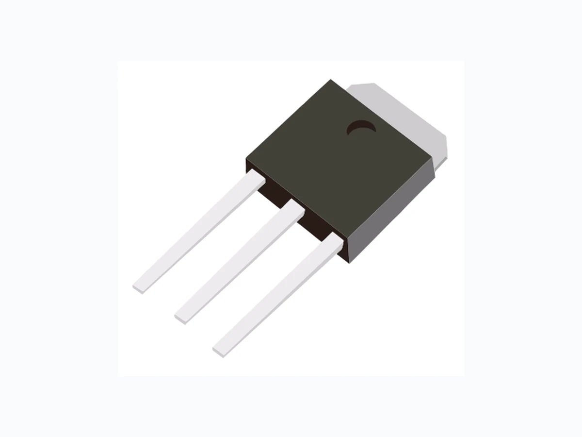
7N65 EVVOSEMI
Document overview
- Manufacturer or author: Provided By digicamel.com
- PDF pages: 7
Technical content
1.Gate 3.Source 2.Drain TO-251 -1- Package Halogen-Free Order codes Halogen 7N65 7N65 N/A N/A TO-252 TO-251 Packing 2500 /Realpieces 70 /Tubepieces
- High ef/g222 ciency switch mode power supplies
- Electronic lamp ballasts based on half bridge
- LED power supplies VDSS 650V 1.2Ω 29nC R (on)max( V =10 V)DS @ GS ID Qg@type TO-252 * RDS(ON) = 1.2Ω @VGS = 10 V * Ultra low gate charge * Low reverse transfer Capacitance * Fast switching capability * Avalanche energy tested * Improved dv/dt capability, high ruggedness ABSOLUTE MAXIMUM RATINGS (TC = 25°C, unless otherwise specified) PARAMETER SYMBOL RATINGS UNIT Drain-Source Voltage VDSS 650 V Gate-Source Voltage VGSS ±30 V Avalanche Current (Note 2) IAR 7 A Drain Current Continuous ID 7 A Pulsed (Note 2) IDM 29.6 A Avalanche Energy Single Pulsed (Note 3) E AS 530 mJ Repetitive (Note 2) EAR 14.2 mJ Peak Diode Recovery dv/dt (Note 4) dv/dt 4.5 V/ns Power Dissipation TO-252/251 PD 120 W Junction Temperature TJ +150 °C Storage Temperature TSTG -55 ~ +150 °C Notes: 1. Absolute maximum ratings are those values beyond which the device could be permanently damaged. Absolute maximum ratings are stress ratings only and functional device operation is not implied. 2. Repetitive Rating : Pulse width limited by maximum junction temperature 3. L = 19.5mH, IAS = 7A, VDD = 50V, RG = 25 Ω, Starting TJ = 25°C 4. ISD≤7A, di/dt≤200A/μs, VDD≤BVDSS, Starting TJ = 25°C ORDER INFORMATION FEATURES APPLICATIONS PRODUCT CHARACTERISTICS N-CHANNEL MOSFET 7N65 7N65 7N65 Rev:2022A2
-2- ELECTRICAL CHARACTERISTICS (TC =25°C, unless otherwise specified) PARAMETER SYMBOL TEST CONDITIONS MIN TYP MAX UNIT OFF CHARACTERISTICS Drain-Source Breakdown Voltage BVDSS V GS = 0V, ID = 250μA 650 V Drain-Source Leakage Current IDSS V DS = 650V, VGS = 0V 1 μA Gate- Source Leakage Current Forward IGSS VGS = 30V, VDS = 0V 100 nA Reverse VGS = -30V, VDS = 0V -100 nA Breakdown Voltage Temperature Coefficient △BVDSS/△TJ ID=250μA,Referenced to 25°C 0.67 V/°C ON CHARACTERISTICS Gate Threshold Voltage VGS(TH) V DS = VGS, ID = 250μA 2.0 4.0 V Static Drain-Source On-State Resistance R DS(ON) VGS = 10V, ID = 3.5A Ω DYNAMIC CHARACTERISTICS Input Capacitance CISS VDS=25V, VGS=0V, f=1.0 MHz 1400 pF Output Capacitance COSS 180 pF Reverse Transfer Capacitance CRSS 16 21 pF SWITCHING CHARACTERISTICS Turn-On Delay Time tD(ON) VDD =325V, ID =7.4A, RG =25Ω (Note 1, 2) 70 ns Turn-On Rise Time tR 170 ns Turn-Off Delay Time tD(OFF) 140 ns Turn-Off Fall Time tF 130 ns SWITCHING CHARACTERISTICS Total Gate Charge QG VDS=520V, ID VGS=10 V (Note 1, 2) 29 38 nC Gate-Source Charge QGS 7 nC Gate-Drain Charge QGD 14.5 nC DRAIN-SOURCE DIODE CHARACTERISTICS AND MAXIMUM RATINGS Drain-Source Diode Forward Voltage VSD V GS = 0V, IS = 7A Maximum Continuous Drain-Source Diode Forward Current IS Maximum Pulsed Drain-Source Diode Forward Current I SM 29.6 A Reverse Recovery Time trr VGS = 0V, IS = 7A, dIF / dt = 100A/μs (Note 1) 320 ns Reverse Recovery Charge QRR 2.4 μC Notes: 1. Pulse Test: Pulse width ≤300μs, Duty cycle≤2% 2. Essentially independent of operating temperature 0.94 1.2 1.4 V 7 A = 7A, N-CHANNEL MOSFET 7N65 Rev:2022A2
-3- TEST CIRCUITS AND WAVEFORMS Same Type as D.U.T. L VDDDriver VGS RG VDS D.U.T. + * dv/dt controlled by RG * ISD controlled by pulse period * D.U.T.-Device Under Test Peak Diode Recovery dv/dt Test Circuit P. W. PeriodD=VGS (Driver) ISD (D.U.T.) IFM, Body Diode Forward Current di/dt IRM Body Diode Reverse Current Body Diode Recovery dv/dt Body Diode Forward Voltage Drop VDD 10V VDS (D.U.T.) VGS= P.W. Period Peak Diode Recovery dv/dt Waveforms N-CHANNEL MOSFET 7N65 Rev:2022A2
-4- w TEST CIRCUITS AND WAVEFORMS (Cont.) VGS D.U.T. RG 10V VDS RL Pulse Width≤ 1μs Duty Factor≤0.1% VDD Switching Test Circuit Switching Waveforms 50kΩ 0.3µF DUT Same Type as D.U.T.0.2µF12V VGS 3mA VDS Gate Charge Test Circuit Gate Charge Waveform Unclamped Inductive Switching Test Circuit Unclamped Inductive Switching Waveforms N-CHANNEL MOSFET 7N65 Rev:2022A2
-5- 1 10 VGS Top 15V 10V 6.5V 5.5V Bottom 5V Notes: 1. 250μs pulse test 2. TC=25℃ ID [A] VDS [V] 2 4 6 8 10 0.1 Notes: 1.250μs pulse test 2.VDS=40V 25℃ ID [A] VGS [V] 150℃ 0 1 2 3 4 5 6 0.8 1.0 1.2 Note :Tj=25℃ VGS=10V VGS=20V RDS (on) [ Ω ] ID [A] On-Region Characteristics Transfer Characteristics On-Resistance Variation vs. Drain Current and Gate Voltage Body Diode Forward Voltage Variation vs. Source Current and Temperature Capacitance Characteristics Gate Charge Characteristics 0.1 Notes: 1. 250μs pulse test 2. VGS =0V 25℃ 150℃ VSD [V] IDR [A] -75 -50 -25 0 25 50 75 100 125 150 0.8 0.9 1.0 1.1 1.2 Notes: 1. VGS=0V 2. ID=250μA BVDS (Normalized) Tj [℃] Breakdown Voltage Variation vs. Temperature On-Resistance Variation vs. Temperature ELECTRICAL CHARACTERISTICS N-CHANNEL MOSFET 7N65 Rev:2022A2
-6- /c110TO- 251 N-CHANNEL MOSFET 7N65 Rev:2022A2
-7- /c110TO- 252 N-CHANNEL MOSFET 7N65 Rev:2022A2