

 Download PDF
7N65_V01 SY
Document overview
- Manufacturer or author: Provided By digicamel.com
- PDF pages: 9
Technical content
Features
RDSON≤1.4Ω @Vgs=10V, Id=3.5A Low gate Charge(typical 23.05nC) Low Crss (typical 2.2pF) Fast switching capability 100% avalanche tested Improved dv/dt capability
Applications
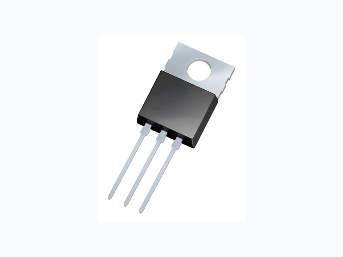
Switch Mode Power Supply (SMPS) Uninterruptible Power Supply (UPS) Power Factor Correction (PFC) (PFC) Charger Key Performance Parameters Parameter Value Unit VDS @ TJ,max 700 V RDS(on),max 1.4 Ω Qg,typ 23.1 nC ID 7 A ID,pulse 28 A Device Marking and Package Information Device Package Marking 7N65 TO-252 7N65AD 7N65 TO-220F 7N65AF 7N65 TO-220 7N65AP 650V N-Channel Planar MOSFET Drain Source Gate TO-252 TO-220F TO -220 7N65
Absolute Maximum Ratings TC = 25º C,unless otherwise noted Parameter Symbol Value Unit Drain-Source Voltage(VGS=0V) VDS 650 V Continuous Drain Current1) TC = 25ºC ID A TC = 100ºC 4.2 Pulsed Drain Current2) ID,pulse 28 A Gate-Source Voltage VGS ±30 V Single Pulse Avalanche Energy3) EAS 211 mJ MOSFET dv/dt Ruggedness, VDS = 0...480V dv/dt 5 V/ns Power Dissipation For TO-220F、TO220-FT PD 78 W Power Dissipation For TO-252、TO-220、TO-251 104 W Continuous Diode Forward Current IS 7 A Diode Pulsed Current2) IS,pulse 28 Operating Junction and Storage Temperature Range TJ, Tstg -55~+150 ºC Notes 1) Limited by maximum junction temperature. 2) Repetitive Rating: Pulse width limited by maximum junction temperature. 3)L=10mH, ID=5.5A, Start TJ=25℃ Thermal Resistance For TO-220F、TO-220FT Parameter Symbol Value Unit Thermal Resistance, Junction-to-Case RthJC 1.6 ºC/W Thermal Resistance, Junction-to-Ambient RthJA 80 Thermal Resistance For TO-252、TO-220、TO-251 Parameter Symbol Value Unit Thermal Resistance, Junction-to-Case RthJC 1.2 ºC/W Thermal Resistance, Junction-to-Ambient RthJA 62 7N65
Electrical Characteristics TJ = 25ºC, unless otherwise noted Parameter Symbol Test Conditions Value Unit Min. Typ. Max. Static Characteristics Drain-Source Breakdown Voltage V(BR)DSS VGS = 0V, ID = 250µ A 650 -- -- V Zero Gate Voltage Drain Current IDSS VDS = 650V VGS = 0V, TJ = 25ºC -- -- 1 μA VDS = 650V, VGS = 0V, TJ = 150ºC -- -- 100 Gate-Source Leakage Current IGSS VGS = ±30V -- -- ±100 nA Gate-Source Threshold Voltage VGS(th) VDS = VGS, ID = 250µ A 2 -- 4 V Drain-Source On-State-Resistance RDS(on) VGS = 10V, ID = 3.5A -- 1.2 1.4 Ω Gate Resistance RG f = 1.0MHz open drain -- 1.7 -- Ω Dynamic Characteristics Input Capacitance Ciss VGS = 0V, VDS =25V f = 1.0MHz -- 1191 -- pFOutput Capacitance Coss -- 86 -- Reverse Transfer Capacitance Crss -- 3 -- Total Gate Charge Qg VDD = 520V, ID = 7A VGS = 10V -- 25.9 -- nCGate-Source Charge Qgs -- 7.1 -- Gate-Drain Charge Qgd -- 8.0 -- Gate Plateau Voltage VPlateau -- 4.9 -- V Turn-on Delay Time td(on) VDD = 325V, ID = 7A RG = 25Ω -- 20 ns Turn-on Rise Time tr -- 50 Turn-off Delay Time td(off) -- 90 Turn-off Fall Time tf -- 55 Drain-Source Body Diode Characteristics Body Diode Forward Voltage VSD TJ = 25ºC, ISD = 7A VGS = 0V -- -- 1.2 V Reverse Recovery Time trr VR = 400V IF = 7A, diF/dt = 100A/μs -- 351 -- ns Reverse Recovery Charge Qrr -- 3.3 -- μC 7N65
Figure A:Gate Charge Test Circuit and Waveform Figure B:Resistive Switching Test Circuit and Waveform Figure C:Unclamped Inductive Switching Test Circuit and Waveform 7N65
A 2.2 2.3 2.4 A1 0 -- 0.2 A2 0.9 1.035 1.17 b 0.645 -- 0.9 b3 5.13 5.326 5.46 c 0.43 -- 0.61 c2 0.41 -- 0.61 D 5.98 6.1 6.22 D1 5.244 -- -- E 6.4 6.6 6.73 E1 4.63 -- -- e 2.186 2.286 2.386 H 9.4 10.04 10.5 L 1.38 1.5 1.75 L1 2.6 2.872 3 L2 0.5 0.509 0.52 L3 0.88 -- 1.28 L4 0.5 -- 1 L6 1.5 1.7 1.95 Ɵ 0° -- 10° 7N65
A 4.5 4.7 4.9 A1 2.34 2.54 2.74 A3 2.56 2.76 2.96 b 0.7 --- 0.95 b1 1.18 --- 1.43 b2 --- --- 1.55 c 0.4 0.5 0.65 D 15.57 15.87 16.17 D1 15.35 15.675 15.95 D2 9.6 9.875 10.15 E 9.96 10.16 10.36 e 2.54 BSC H1 6.48 6.68 6.88 L 12.68 12.98 13.28 L1 --- --- 3.5 7N65
A 2.20 2.30 2.38 A1 0.90 1.04 1.17 b 0.56 -- 0.90 b4 5.20 5.33 5.46 b5 -- -- 1.05 c 0.43 -- 0.61 c2 0.43 -- 0.61 D 5.98 6.10 6.22 D1 5.2 -- -- E 6.40 6.60 6.73 E1 4.60 -- -- e 2.24 2.29 2.34 e1 4.47 4.57 4.67 H 16.18 16.50 16.82 L 9 9.35 9.65 L2 0.88 1.05 1.28