

 Download PDF
7N65 DYELEC
Document overview
- Manufacturer or author: Provided By digicamel.com
- PDF pages: 9
Technical content
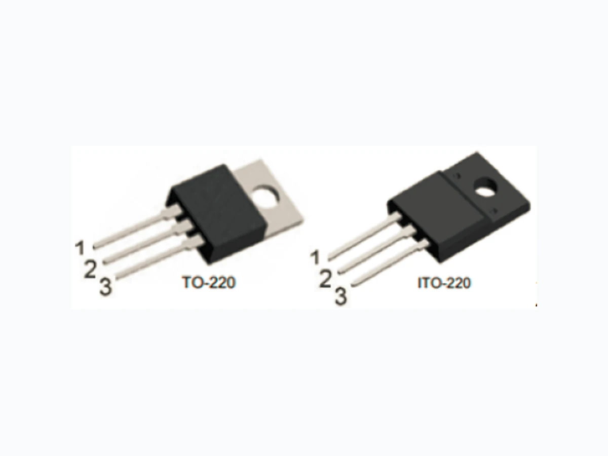
1 / 9May.2015-REV.00 www.dyelec.com 1. Gate 2. Drain 3. Source Pin Definition: PRODUCT SUMMARY VDS (V) RDS(on)(Ω) ID (A) 650 1.5 @ VGS =10V 7 650V N-Channel Power MOSFET ABSOLUTE MAXIMUM RATINGS (TC=25°C, unless otherwise specified) RDS(ON)<1.5Ω @ VGS=10V Fast switching capability Low gate charge Lead free in compliance with EU RoHS directive. Green molding compound Block Diagram
Ordering Information
- Case:TO-220,ITO-220,TO-262,TO-263 Package D G S PARAMETER SYMBOL RATINGS UNIT Drain-Source Voltage VDSS 650 V Gate-Source Voltage VGSS ±30 V Continuous Drain Current ID 7 A Pulsed Drain Current (Note 2) IDM 28 A Avalanche Energy Single Pulsed (Note 3) E AS 435 mJ Power Dissipation TO-220/TO-262/TO-263 PD 142 W ITO-220 48 W Junction Temperature TJ +150 °C Storage Temperature TSTG -55 ~ +150 °C Notes: 1. Absolute maximum ratings are those values beyond which the device could be permanently damaged. Absolute maximum ratings are stress ratings only and functional device operation is not implied. 2. Repetitive Rating : Pulse width limited by TJ 3. L = 30mH, IAS = 5.25A, VDD = 50V, RG = 25 Ω, Starting TJ = 25°C Part No. Package Packing DMT7N65-TU TO-220 50pcs / Tube DMF7N65-TU ITO-220 50pcs / Tube DMK7N65-TU TO-262 50pcs / Tube DMG7N65-TU TO-263 50pcs / Tube DMG7N65-TR TO-263 800pcs / 13" Reel
650V N-Channel Power MOSFET ELECTRICAL CHARACTERISTICS (TC=25°C, unless otherwise specified) PARAMETER SYMBOL RATING UNIT Junction to Ambient TO-220/ITO-220 TO-262/TO-263 θJA 62.5 °C/W Junction to Case TO-220/TO-262/TO-263 θJC 0.90 °C/W ITO-220 2.6 PARAMETER SYMBOL T EST CONDITIONS TYP MIN MAX UNIT OFF CHARACTERISTICS Drain-Source Breakdown Voltage BVDSS GSV =0V, ID=250μA 650 V Drain-Source Leakage Current IDSS VDS=650V, VGS=0V 1 μA Gate- Source Leakage Current Forward IGSS VG=30V, VDS=0V 100 nA Reverse VGS=-30V, VDS=0V -100 nA Breakdown Voltage Temperature Coefficient △BVDSS/△TJ ID=250μA, Referenced to 25°C 0.67 V/°C ON CHARACTERISTICS Gate Threshold Voltage VGS(TH) DSV =VGS, ID=250μA 2.0 4.0 V Static Drain-Source On-State Resistance R DS(ON) 1.35 1.5 Ω DYNAMIC CHARACTERISTICS Input Capacitance CISS VDS=25V, VGS =0V, f=1.0 MHz 1210 1400 pF Output Capacitance COSS pF140 180 Reverse Transfer Capacitance CRSS 40 50 pF SWITCHING CHARACTERISTICS Turn-On Delay Time tD(ON) 50 70 ns Turn-On Rise Time tR ns150 180 Turn-Off Delay Time tD(OFF) 380 410 ns Turn-Off Fall Time tF 180 220 ns Total Gate Charge QG 29 38 nC Gate-Source Charge QGS nC9 Gate-Drain Charge QGD 19 nC DRAIN-SOURCE DIODE CHARACTERISTICS AND MAXIMUM RATINGS Drain-Source Diode Forward Voltage VSD 1.4 V Maximum Continuous Drain-Source Diode Forward Current IS 7 A Maximum Pulsed Drain-Source Diode Forward Current I SM 28 A Reverse Recovery Time trr VGS=0V, IS=7.0A, dIF/dt =100 A/μs (Note 1) 490 ns Reverse Recovery Charge QRR μC3.2 Notes: 1. Pulse Test: Pulse width ≤ 300μs, Duty cycle ≤ 2%. 2. Essentially independent of operating temperature. May.2015-REV.00 www.dyelec.com V GS= 10V, ID = 3.5A VDD =300V, ID =7A, RG =25Ω (Note 1, 2) VDS=520V, ID=7A, VGS=10V (Note 1, 2) VGS=0V, IS = 7A
TEST CIRCUITS AND WAVEFORMS 600V N-Channel Power MOSFET Same Type as D.U.T. L VDDDriver VGS RG VDS D.U.T. + * dv/dt controlled by RG * SD controlled by pulse period * D.U.T.-D vice Under Test Peak Diode Recovery dv/dt Test Circuit P. W. PeriodD=VGS (Driver) ISD (D.U.T.) IFM, Body Diode Forward Current di/dt IRM Body Diode Reverse Current Body Diode Recovery dv/dt Body Diode Forward Voltage Drop VDD 10V VDS (D.U.T.) VGS= P.W. Period Peak Diode Recovery dv/dt Waveforms May.2015-REV.00 www.dyelec.com 7N65
TEST CIRCUITS AND WAVEFORMS(Cont.) 650V N-Channel Power MOSFET Switching Test Circuit Switching Waveforms Gate Charge Test Circuit Gate Charge Waveform VDD BVDSS IAS ID(t) VDS(t) Unclamped Inductive Switching Test Circuit tp Time Unclamped Inductive Switching Waveforms Jan.2015-REV.00 www.sddydz.com May.2015-REV.00 www.dyelec.com 7N65
650V N-Channel Power MOSFET May.2015-REV.00 www.dyelec.com 7N65 Drain-Source On-Resistance, RDS(ON) (Ω) Drain Current, ID (A) On-Resistance Variation vs. Drain Current and Gate Voltage 6 8 10 12 0.1 Source-Drain Voltage, VSD (V) Reverse Drain Current, IDR (A) On State Current vs. Allowable Case Temperature 0.6 Note: TJ=25°C Notes: 1. . GS=0V 2. 250µs Test VGS=20V VGS=10V
650V N-Channel Power MOSFET 7N65 6 / 9 May.2015-REV.00 www.dyelec.com Drain-Source Breakdown Voltage, BVDSS (Normalized) Drain-Source On-Resistance, RDS(ON) (Normalized) Square Wave Pulse Duration, t1 (sec) Transient Thermal Response Curve Case Temperature, TC (°C) 75 100 12550 25 2.5 3.75 5.0 6.25 7.5 Maximum Drain Current vs. Case Temperature 1.25 150 0.1 0.01 10-5 10-4 10-3 10-2 10-1 100 101 Notes: 1. θJC (t) ) = 1 18°C/W Max. 2. Duty Factor, D=t1/t2 3. TJM-TC=PDM×θJC (t) D=0.5 0.2 0.1 0.05 0.02 0.01 Single Pulse 100 10-1 10-2 Drain-Source Voltage, VDS (V) 102101100 103 Safe Operating Area – 650V Notes: 1. TJ=25°C 2. TJ=150°C 3. Single Pulse DC 10ms 1ms 100µs Operation in This Area is Limited by RDS(on) 101 650
650V N-Channel Power MOSFET May.2015-REV.00 www.dyelec.com 7N65 TO-220 Mechanical Drawing TO-220 Mechanical Drawing ITO-220 Mechanical Drawing
650V N-Channel Power MOSFET 8 / 9 May,2015-REV.00 www.dyelec.com TO-262 Mechanical Drawing TO-263 Mechanical Drawing
Specifications of the products displayed herein are subject to change without notice. DIYI or anyone on its behalf, assumes no responsibility or liability for any errors or inaccuracies. Information contained herein is intended to provide a product description only. No license, express or implied, to any intellectual property rights is granted by this document. Except as provided in DIYI’s terms and conditions of sale for such products, DIYI assumes no liability whatsoever, and disclaims any express or implied warranty, relating to sale and/or use of DIYI products including liability or warranties relating to fitness for a particular purpose, merchantability, or infringement of any patent, copyright, or other intellectual property right. The products shown herein are not designed for use in medical, life-saving, or life-sustaining applications. Customers using or selling these products for use in such applications do so at their own risk and agree to fully indemnify DIYI for any damages resulting from such improper use or sale. 650V N-Channel Power MOSFET May.2015-REV.00 www.dyelec.com 7N65