Download PDF
DATASHEET SEARCH SITE
Document overview
- PDF pages: 3
Technical content
Page 1
3-terminal 1 A positive voltage regulator
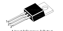
Features
- Output Current up to 1 A
- Thermal Overload Protection
- Short Circuit Protection
- Output Transistor Safe Operating Area Protection
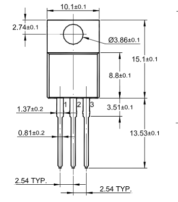
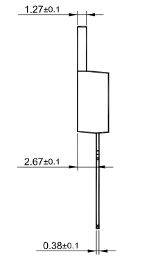
TO-220 Plastic Package
Absolute Maximum Ratings (Ta = 25 OC)
| Parameter | Symbol | Value | Unit |
|---|---|---|---|
| Input Voltage | V I | 35 | V |
| Thermal Resistance Junction-Cases | R θJC | 5 | OC/W |
| Thermal Resistance Junction-Air | R θJA | 65 | OC/W |
| Operating Temperature Range | T OPR | 0 to + 125 | OC |
| Storage Temperature Range | T S | - 65 to + 150 | OC |
Electrical Characteristics
(0 OC < TJ < 125 OC, IO = 500 mA, VI = 16 V, CI = 0.33 µF, CO = 0.1 µF, unless otherwise specified)
| Parameter | Symbol | Conditions | Min. | Typ. | Max. | Unit | |
|---|---|---|---|---|---|---|---|
| Output Voltage | V O | T = 25 OC J | 9.6 | 10 | 10.4 | V | |
| 5 mA I 1 A, P 15 W O O V = 12.5 V to 25 V I | 9.5 | 10 | 10.5 | ||||
| Line Regulation 1) | Regline | T = 25 OC J | V = 12.5 V to 25 V I | - | - | 200 | mV |
| V = 13 V to 20 V I | - | - | 100 | ||||
| Load Regulation 1) | Regload | T = 25 OC J | I = 5 mA to 1.5 A O | - | - | 200 | mV |
| I = 250 mA to 750 mA O | - | - | 100 | ||||
| Quiescent Current | I Q | T = 25 OC J | - | - | 8 | mA | |
| Quiescent Current Change | I Q | I = 5 mA to 1 A O | - | - | 0.5 | mA | |
| V = 13 V to 29 V I | - | - | 1 | ||||
| Output Voltage Drift | V /T O | I = 5 mA O | - | -1 | - | mV/OC | |
| Output Noise Voltage | V N | f = 10 Hz to 100 KHz, T = 25 OC a | - | 58 | - | µV | |
| Ripple Rejection | RR | f = 120 Hz, V = 14 V to 24 V I | 56 | - | - | dB | |
| Dropout Voltage | V Drop | I = 1 A, T = 25 OC O J | - | 2 | - | V | |
| Output Resistance | R O | f = 1 KHz | - | 17 | - | mΩ | |
| Short Circuit Current | I SC | V = 35 V, T = 25 OC I a | - | 250 | - | mA | |
| Peak Current | I PK | T = 25 OC J | - | 2.2 | - | A | |
1) Load and line regulation are specified at constant junction temperature, Changes in VO due to heating effects must be taken into account separately, Pulse testing with low duty is used.
Page 2
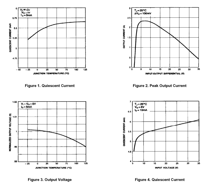
Typical Performance Characteristics
Page 3
TO-220 PACKAGE OUTLINE