


 Download PDF
DATASHEET SEARCH SITE
Document overview
- PDF pages: 45
Technical content
Page 1

PAC1934
Evaluation Board (ADM00805)
User’s Guide
DS50002673A
Page 2


Information contained in this publication regarding device applications and the like is provided only for your convenience and may be superseded by updates. It is your responsibility to ensure that your application meets with your specifications. MICROCHIP MAKES NO REPRESENTATIONS OR WARRANTIES OF ANY KIND WHETHER EXPRESS OR IMPLIED, WRITTEN OR ORAL, STATUTORY OR OTHERWISE, RELATED TO THE INFORMATION, INCLUDING BUT NOT LIMITED TO ITS CONDITION, QUALITY, PERFORMANCE, MERCHANTABILITY OR FITNESS FOR PURPOSE. Microchip disclaims all liability arising from this information and its use. Use of Microchip devices in life support and/or safety applications is entirely at
the buyer’s risk, and the buyer agrees to defend, indemnify and hold harmless Microchip from any and all damages, claims, suits, or expenses resulting from such use. No licenses are conveyed, implicitly or otherwise, under any Microchip intellectual property rights unless otherwise stated.
Microchip received ISO/TS-16949:2009 certification for its worldwide headquarters, design and wafer fabrication facilities in Chandler and Tempe, Arizona; Gresham, Oregon and design centers in California and India. The Company’s quality system processes and procedures are for its PIC® MCUs and dsPIC® DSCs, KEELOQ® code hopping devices, Serial EEPROMs, microperipherals, nonvolatile memory and analog products. In addition, Microchip’s quality system for the design and manufacture of development systems is ISO 9001:2000 certified.
| QUALITY MANAGEMENT SYSTEM CERTIFIED BY DNV == ISO/TS 16949 == | respective companies. © 2017, Microchip Technology Incorporated, All Rights Reserved. ISBN: 978-1-5224-2155-9 |
DS50002673A-page 2
Page 3
Object of Declaration: PAC1934 Evaluation Board (ADM00805) User’s Guide
EU Declaration of Conformity
This declaration of conformity is issued by the manufacturer. The development/evaluation tool is designed to be used for research and development in a laboratory environment. This development/evaluation tool is not a Finished Appliance, nor is it intended for incorporation into Finished Appliances that are made commercially available as single functional units to end users under EU EMC Directive 2004/108/EC and as supported by the European Commission's Guide for the EMC Directive 2004/108/EC (8th February 2010). This development/evaluation tool complies with EU RoHS2 Directive 2011/65/EU. This development/evaluation tool, when incorporating wireless and radio-telecom functionality, is in compliance with the essential
requirement and other relevant provisions of the R&TTE Directive 1999/5/EC and the FCC rules as stated in the declaration of conformity provided in the module datasheet and the module product page available at www.microchip.com. For information regarding the exclusive, limited warranties applicable to Microchip products, please see Microchip’s standard terms and conditions of sale, which are printed on our sales documentation and available at www.microchip.com. Signed for and on behalf of Microchip Technology Inc. at Chandler, Arizona, USA.

DS50002673A-page 3
Page 4
NOTES:
DS50002673A-page 4
Page 5

PAC1934 EVALUATION BOARD
(ADM00805) USER’S GUIDE
Table of Contents
Preface ........................................................................................................................... 7
Introduction............................................................................................................ 7 Document Layout .................................................................................................. 7 Conventions Used in this Guide............................................................................ 8 Warranty Registration............................................................................................ 8 Recommended Reading........................................................................................ 9 The Microchip Web Site ........................................................................................ 9
Product Change Notification Service..................................................................... 9 Customer Support ................................................................................................. 9 Document Revision History ................................................................................... 9
Chapter 1. Product Overview
1.1 Introduction ................................................................................................... 11 1.2 PAC1934 Device Features ........................................................................... 11 1.3 ADM00805 Evaluation Board for PAC1934 ................................................. 11 1.3.1 Hardware Overview ................................................................................... 11 1.3.2 Software and System Control Overview .................................................... 12 1.4 Evaluation Board Kit Contents ..................................................................... 12
Chapter 2. Installation and Operation
2.1 Getting Started ............................................................................................. 13 2.2 System Requirements .................................................................................. 13 2.3 Installing the Software .................................................................................. 13
Chapter 3. Software GUI Description
3.1 First Launch .................................................................................................. 17 3.2 Top Menu ..................................................................................................... 20 3.3 PAC Settings Section ................................................................................... 22 3.3.1 Alert Settings ............................................................................................. 22 3.4 Sample Rate and Display Controls .............................................................. 23 3.5 Raw Data Display ......................................................................................... 24
3.6 Plot Windows ................................................................................................ 24 3.6.1 Single Plot Option ...................................................................................... 24 3.6.2 Multiple Plots Option ................................................................................. 26
Chapter 4. Hardware Description
4.1 Default Connections, DEMO Mode and System Mode ................................ 27 4.2 Default Connections, DEMO Mode and System Mode for Channel Inputs .. 27 4.3 VBUS and VSENSE Connections - Using External Sources for SYTSTEM Mode ....................................................................................................... 28
DS50002673A-page 5
Page 6
4.4 Other Hardware on the Board ...................................................................... 28 4.5 Hardware for I2C/SMBus Communication over USB or External I2C Connection ......................................................................................29 4.6 Signal Description in DEMO MODE ............................................................. 29 4.7 PAC1934 Current Measurements using the PAC1934. ............................... 29 4.8 Additional Hardware Details ......................................................................... 30 4.9 Direct External I2C Connection .................................................................... 31
4.10 Jumper Connections - Default Configuration and Other Information Tabulated .........................................................................................31
Appendix A. Schematic and Layouts
A.1 Introduction .................................................................................................. 33 A.2 ADM00805 Evaluation Board - Schematic ................................................... 34 A.3 ADM00805 Evaluation Board - Schematic 2 ................................................ 35 A.4 ADM00805 Evaluation Board - Schematic 3 ................................................ 36 A.5 Board - Top Silk ........................................................................................... 37 A.6 Board - Top Copper and Silk ....................................................................... 37 A.7 Board - Top Copper ..................................................................................... 38
A.8 Board - Bottom Copper ................................................................................ 38 A.9 Board - Bottom Copper and Silk .................................................................. 39 A.10 Board - Bottom Silk .................................................................................... 39
Appendix B. Bill of Materials (BOM) Worldwide Sales and Service .....................................................................................44
DS50002673A-page 6
Page 7

PAC1934 EVALUATION BOARD
(ADM00805) USER’S GUIDE
Preface
INTRODUCTION
This chapter contains general information that will be useful to know before using the ADM00805. Items discussed in this chapter include:
- Document Layout
- Conventions Used in this Guide
- Warranty Registration
- Recommended Reading
- The Microchip Web Site
- Customer Support
- Document Revision History
DOCUMENT LAYOUT
This document describes how to use the ADM00805 Evaluation Board as a development tool to emulate and debug firmware on a target board. The manual layout is as follows:
- Chapter 1. “Product Overview” – Important information about the ADM00805 Evaluation Board.
- Chapter 2. “Installation and Operation” – Includes instructions on installing and starting the PAC193X Demo Application.
- Chapter 3. “Software GUI Description” – Includes details about the GUI.
- Chapter 4. “Hardware Description” – Detailed information about the PAC1934 device and the ADM00805 Evaluation Board.
- Appendix A. “Schematic and Layouts” – Shows the schematic and layout diagrams for the ADM00805 Evaluation Board.
- Appendix B. “Bill of Materials (BOM)” – Lists the parts used to build the ADM00805 Evaluation Board.
DS50002673A-page 7
Page 8
CONVENTIONS USED IN THIS GUIDE
This manual uses the following documentation conventions:
DOCUMENTATION CONVENTIONS
| Description | Represents | Examples |
|---|---|---|
| Arial font: | ||
| Italic characters | Referenced books | MPLAB® IDE User’s Guide |
| Emphasized text | ...is the only compiler... | |
| Initial caps | A window | the Output window |
| A dialog | the Settings dialog | |
| A menu selection | select Enable Programmer | |
| Quotes | A field name in a window or dialog | “Save project before build” |
| Underlined, italic text with right angle bracket | A menu path | File>Save |
| Bold characters | A dialog button | Click OK |
| A tab | Click the Power tab | |
| N‘Rnnnn | A number in verilog format, where N is the total number of digits, R is the radix and n is a digit. | 4‘b0010, 2‘hF1 |
| Text in angle brackets < > | A key on the keyboard | Press <Enter>, <F1> |
| Courier New font: | ||
| Plain Courier New | Sample source code | #define START |
| Filenames | autoexec.bat | |
| File paths | c:\mcc18\h | |
| Keywords | _asm, _endasm, static | |
| Command-line options | -Opa+, -Opa- | |
| Bit values | 0, 1 | |
| Constants | 0xFF, ‘A’ | |
| Italic Courier New | A variable argument | file.o, where file can be any valid filename |
| Square brackets [ ] | Optional arguments | mcc18 [options] file [options] |
| Curly brackets and pipe character: { | } | Choice of mutually exclusive arguments; an OR selection | errorlevel {0|1} |
| Ellipses... | Replaces repeated text | var_name [, var_name...] |
| Represents code supplied by user | void main (void) { ... } | |
DS50002673A-page 8
Page 9
Preface
RECOMMENDED READING
This user’s guide describes how to use the ADM00805. Other useful documents are listed below. The following Microchip document is available and recommended as a supplemental reference resource:
PAC1934 Data Sheet – “DC Power/Energy Monitor with Accumulator” (DS20005850A)
THE MICROCHIP WEB SITE
Microchip provides online support via our web site at www.microchip.com. This web site is used as a means to make files and information easily available to customers. Accessible by using your favorite Internet browser, the web site contains the following information:
- Product Support – Data sheets and errata, application notes and sample programs, design resources, user’s guides and hardware support documents, latest software releases and archived software
- General Technical Support – Frequently Asked Questions (FAQs), technical support requests, online discussion groups, Microchip consultant program member listing
- Business of Microchip – Product selector and ordering guides, latest Microchip press releases, listing of seminars and events, listings of Microchip sales offices, distributors and factory representatives
PRODUCT CHANGE NOTIFICATION SERVICE
Microchip’s customer notification service helps keep customers current on Microchip products. Subscribers will receive e-mail notifications whenever there are changes, updates, revisions or errata related to a specified product family or development tool of interest. To register, access the Microchip web site at www.microchip.com, click on Product Change Notification and follow the registration instructions.
CUSTOMER SUPPORT
Users of Microchip products can receive assistance through several channels:
- Distributor or Representative
- Local Sales Office
- Field Application Engineer (FAE)
- Technical Support Customers should contact their distributor, representative or field application engineer (FAE) for support. Local sales offices are also available to help customers. A listing of sales offices and locations is included in the back of this document. Technical support is available through the web site at: http://www.microchip.com/support.
DOCUMENT REVISION HISTORY
Revision A (September 2017)
- Initial Release of this Document.
DS50002673A-page 9
Page 10
NOTES:
DS50002673A-page 10
Page 11

PAC1934 EVALUATION BOARD
(ADM00805) USER’S GUIDE
Chapter 1. Product Overview
1.1 INTRODUCTION
The ADM00805 Evaluation Board for PAC1934 provides a flexible platform for evaluating PAC1934 and demonstrating the features of the PAC1934. A PAC1934 device in a wafer level chip scale package (WLCSP) is mounted to the board. The ADM00805 has a USB connector to connect to a computer for device communication. The PAC1934 device may be powered directly by VBUS from the USB connector or by an external connection for VDD. I2C communication can be provided over USB using the on-board MCP2221 USB to I2C Bridge. There is also a header that facilitates direct I2C communication by connecting the VDD_IO, Ground, SDA and SCL to an external source such as a PC motherboard
or a Linux system. See Section 4.9 “Direct External I2C Connection” for important details if using direct I2C connection. The shorting shunts and the switch on the board facilitate either simple demonstration of the device functions using on-board current sources or detailed evaluation of function and performance with external sources, including prototyping the system.
1.2 PAC1934 DEVICE FEATURES
The PAC1934 is a four-channel DC power/energy monitor with accumulator. There is a16-bit ADC for monitoring power rail voltages connected by a multiplexer to the positive (+) input pin of each channel, producing results named VBUS. There is a second 16-bit ADC for measuring the voltage across a current sense resistor. This ADC is connected by a differential multiplexer to the +input and –input pins for each channel, producing results called VSENSE. Channel selection for the multiplexers is controlled in sequential fashion to scan all four channels up to 1024 samples per second (sps). The device also computes VPOWER by multiplying VBUS by VSENSE and accumulates
these power results in an Accumulator. The device registers also hold eight times averaged VBUS and VSENSE results for very accurate low noise voltage and current measurements. All the results are stored in registers. The values in the Results Registers only change when a REFRESH or a REFRESH_V command is sent. Software applications are available for plotting, displaying and logging data. These applications also calculate energy based on the accumulated power and accumulation time.
1.3 ADM00805 EVALUATION BOARD FOR PAC1934
1.3.1 Hardware Overview
The ADM00805 Evaluation Board has a PAC1934 device mounted on the board and enables direct control of all device pins and easy measurements of on-board or external voltages and currents. The I2C address is connected as 0x20 by default. Removing a shunt gives 0x22. Other addresses are possible by replacing R22 with a new value. Sampling rate is 1024 sps by default, due to the shorting shunt on the SLOW pin connector (J23) tying the SLOW pin to ground. Remove this shunt for the SLOW sampling rate of 8 sps.
DS50002673A-page 11
Page 12
An on-board current source provides a 0.5 Hz square wave current signal for functionality testing and demo purposes. There are also on-board current sense resistors, provisions for external sources and loads, and provisions for both USB control and direct I2C connection. See Chapter 4. “Hardware Description” for more details.
Software and System Control Overview 1.3.2
The PAC193X Demo Application, described in detail in Chapter 2. “Installation and Operation”, provides USB control of the PAC193X with the ADM00805 Evaluation Board. The application provides an easy way to control all of the programmable registers and read all of the results for the PAC1934 device on the ADM00805 Evaluation Board. To use this software application with the ADM00805 Evaluation Board, download the software and launch the application. Then connect the provided USB cable to the computer and ensure that the USB/I2C switch is set ON. Chapter 2. “Installation and Operation” provides details on getting started.
1.4 EVALUATION BOARD KIT CONTENTS
The PAC1934 Evaluation Board Kit contains:
- The ADM00805 Evaluation Board (EVB)
- USB cable
- Important Information Sheet
DS50002673A-page 12
Page 13

PAC1934 EVALUATION BOARD
(ADM00805) USER’S GUIDE
Chapter 2. Installation and Operation
2.1 GETTING STARTED
This section describes how to power-up and interface with the ADM00805 Evaluation Board. Items discussed in this chapter include:
- System requirements
- Downloading and installing the software
2.2 SYSTEM REQUIREMENTS
The ADM00805 Evaluation Board is designed to be used with a personal computer (desktop or laptop) running Microsoft® Windows® 7 or later. For USB connectivity, the minimal physical requirement for the PC is a standard type-A USB 2.0 port.
2.3 INSTALLING THE SOFTWARE
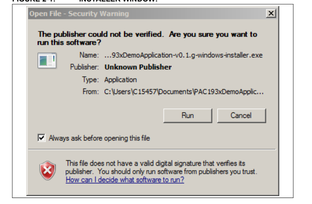
Go to www.microchip.com and search for PAC1934. Select the PAC193X Demo Application and double-click the executable program to download the ZIP file. Extract the files from the ZIP archive. Once the files have been extracted, double-click the application file to begin installing the software. Follow the next steps to proceed with the installation: 1. Figure 2-1 shows the Installer window. Click the Run button. 2. If the used antivirus software presents a warning, allow the file to run in order to proceed with the installation.
INSTALLER WINDOW:
FIGURE 2-1:
DS50002673A-page 13
Page 14
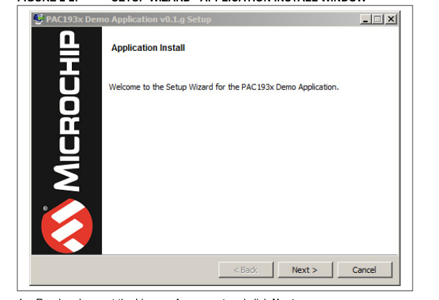
- Figure 2-2 shows the Application Install window. Click the Next button.
SETUP WIZARD - APPLICATION INSTALL WINDOW
FIGURE 2-2:
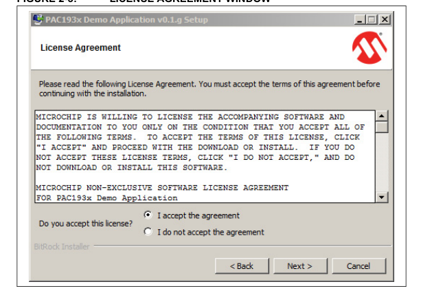
- Read and accept the License Agreement and click Next.
LICENSE AGREEMENT WINDOW
FIGURE 2-3:
DS50002673A-page 14
Page 15
Installation and Operation
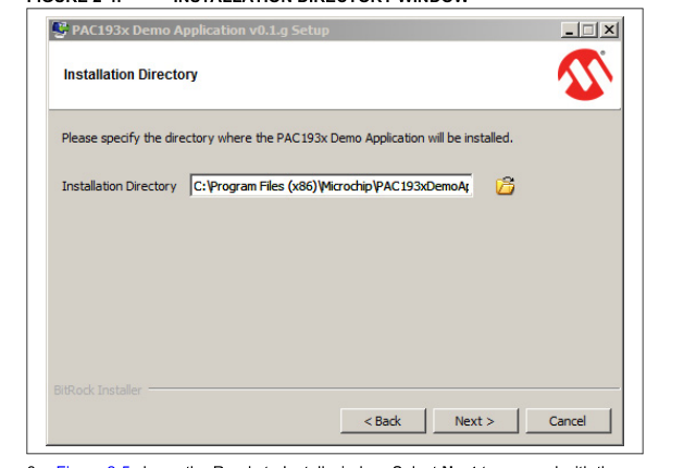
- Select the desired installation directory and click Next.
INSTALLATION DIRECTORY WINDOW
FIGURE 2-4:
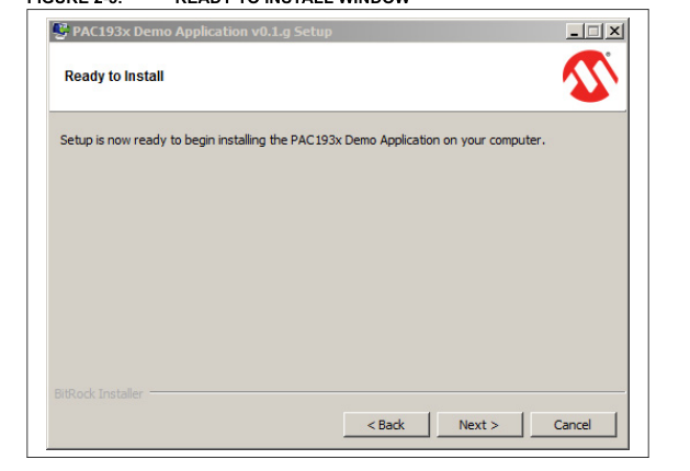
- Figure 2-5 shows the Ready to Install window. Select Next to proceed with the installation.
READY TO INSTALL WINDOW
FIGURE 2-5:
DS50002673A-page 15
Page 16
- Once the setup wizard has finished installing the software, the Install Complete window will appear. Click the Finish button to begin using the application.
INSTALL COMPLETE WINDOW
FIGURE 2-6:
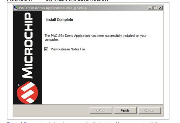
Figure 2-7 shows the desktop icon created by the installer. Hovering over it with the cursor will show the title PAC193X Demo Application.
FIGURE 2-7:
DESKTOP ICON

DS50002673A-page 16
Page 17

PAC1934 EVALUATION BOARD
(ADM00805) USER’S GUIDE
Chapter 3. Software GUI Description
3.1 FIRST LAUNCH
After the installation, double-click the desktop icon in order to launch the PAC193X Demo Application. Connect the board to the computer with the provided USB cable and ensure the USB/I2C switch is set ON. The SW1 switch is in the upper right corner of the board. Once they are connected, LED activity can be seen on the board:
- LD1: shows I2C activity from the USB bridge
- LD2: +5V USB power from the USB connection
- LD3: Shows the period of the square wave generated by the on-board current source
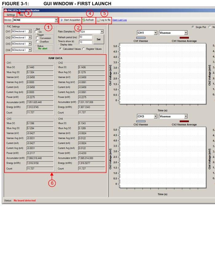
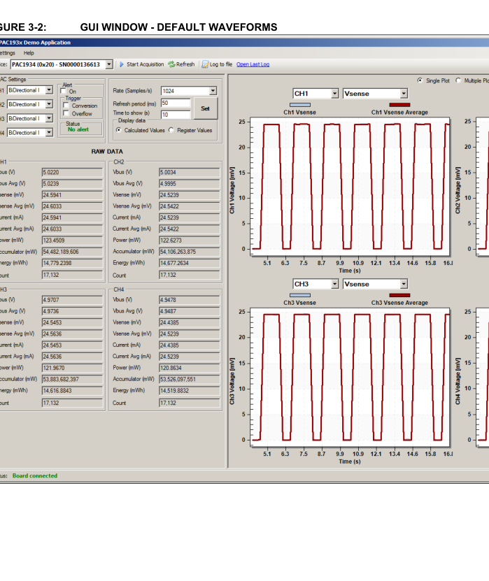
Figure 3-1 shows the GUI for the PAC193X Demo Application: 1. Device identification 2. Start Acquisition button Click the Start Acquisition button to start generating the default waveforms. After 10 seconds, click the button again to stop the acquisition and freeze the waveforms. Figure 3-2 displays the default waveforms in DEMO mode.
DS50002673A-page 17
Page 18
DS50002673A-page 18
Page 19
Software GUI Description
DS50002673A-page 19
Page 20
3.2 TOP MENU
As seen in Figure 3-1, the Device window (1) shows the device on the board and its I2C address; some parts have a serial number that is displayed. When clicked, the Settings button (3) displays a drop-down menu with two options: Set Constants and Slow Register, as shown in Figure 3-3. Note that you need to stop the acquisition process in order to have access to the Slow Register. It is recommended that the acquisition process is stopped before changing the values in the Set Constants Menu. Any changes to these values do not take effect until the start of the acquisition.
SETTINGS DROP-DOWN MENU
FIGURE 3-3:
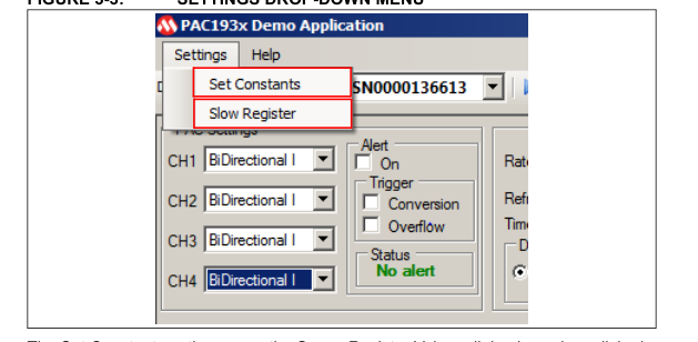
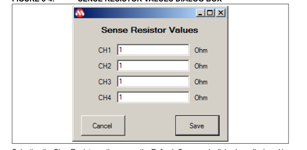
The Set Constants option opens the Sense Resistor Values dialog box when clicked, displayed in Figure 3-4. The default values shown are the sense resistor values in DEMO mode. Enter a new value in ohms if the SYSTEM/SHUNT mode is used or if a different value of sense resistor is used (see Section 3.3 “PAC Settings section”).
SENSE RESISTOR VALUES DIALOG BOX
FIGURE 3-4:
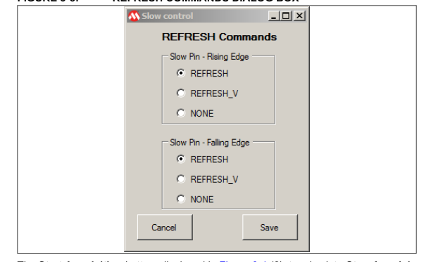
Selecting the Slow Register option opens the Refresh Commands dialog box, displayed in Figure 3-5, which allows the user to select which type of refresh commands, if any, occur on the rising and falling edge of the SLOW pin transitions. Select the desired options and the GUI programs the Slow Register (0x20) in the PAC1934 appropriately (see the
DS50002673A-page 20
Page 21
Software GUI Description
PAC1934 Data Sheet).This register is important if the SLOW pin is being used, the user will be able to capture the data for very accurate energy calculation when switching from a programmed sample rate to the eight samples/second rate under control of the SLOW pin. If the SLOW pin is not being used, these settings can be ignored.
REFRESH COMMANDS DIALOG BOX
FIGURE 3-5:
The Start Acquisition button, displayed in Figure 3-1 (2), toggles into Stop Acquisition when clicked. When the button is clicked, a REFRESH command is sent to the PAC1934 and it starts collecting conversion data in the accumulator. The GUI starts sending REFRESH_V commands to the PAC1934 and reading results data from all of the results registers for data plotting (and logging, if selected). When clicked, the Refresh button, displayed in Figure 3-1 (4), sends a command to the PAC1934, updating the control registers and loading all the results from the ADCs and the accumulator into the readable registers. The refresh command also resets the accumulators and the accumulator count.
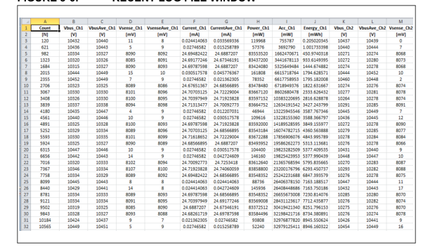
The Log to File button, displayed in Figure 3-1 (5), toggles when clicked to stop the logging to file process and turns data logging on and off. In order to log the data, the user must be acquiring. The data file is a CSV file created in the directory where the GUI has been installed. There is a link next to this button to open the last log. Stop acquiring data before opening the log file. When the Open Last Log button is clicked, the most recent data log is opened. It can be noticed that all of the results data is captured, and each column has a header identifying the data. Figure 3-6 shows one corner of a log file.
DS50002673A-page 21
Page 22
RECENT LOG FILE WINDOW
FIGURE 3-6:
3.3 PAC SETTINGS SECTION
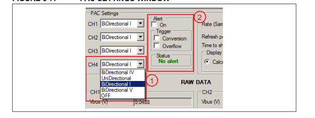
Each input channel of the PAC1934 is internally set for unipolar/unidirectional voltage on VBUS and unidirectional currents on VSENSE by default. However, in the GUI, all four channels are configured for bidirectional currents by default. This bidirectional setting avoids clipping of negative values. For bidirectional currents the VSENSE results are in 16-bit two's complement representation. A drop-down menu allows reconfiguring each channel or turning it off as shown in Figure 3-7 for channel 4 (1). Using the GUI this way programs the appropriate register for the selected channel.
PAC SETTINGS WINDOW
FIGURE 3-7:
3.3.1 Alert Settings
The check boxes enable turning on the alert function and selecting which type of conditions can trigger the alert function: Conversion Complete or Accumulator Overflow. The alert status is also displayed underneath the check boxes, as shown in Figure 3-7 (2). The GUI is not fast enough to capture the conversion based ALERT, which lasts only 5 μS. The SLOW/ALERT pin must be monitored with a circuit fast enough to detect the 5 μS wide ALERT signal to use this function.
DS50002673A-page 22
Page 23
Software GUI Description
3.4 SAMPLE RATE AND DISPLAY CONTROLS
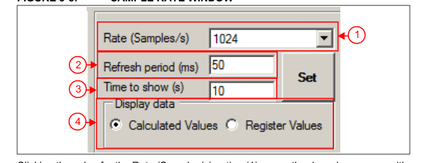
Figure 3-8 shows the Sample Rate window, located to the right of the Alert window.
SAMPLE RATE WINDOW
FIGURE 3-8:
Clicking the value for the Rate (Samples/s) option (1) opens the drop-down menu with the available programmable sample rates for the PAC1934, shown in Figure 3-9. Sleep mode and One Shot mode are two of the options that can be selected. In One Shot mode, a new round of results are collected when a refresh command is sent with the Refresh button right above the Sample Rate window.
SAMPLE RATE WINDOW - DROP-DOWN MENU
FIGURE 3-9:
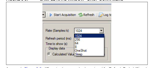
As seen in Figure 3-8, different values can also be entered for Refresh Period (2) and Time to Show (3). Refresh Period determines how often the GUI reads the results from the PAC1934. This is limited to 50 ms maximum by the ADM00805 Evaluation Board hardware, not the PAC1934. The GUI performs the reading by sending a REFESH_V command to the PAC1934 and then reads all of the results registers. Time to Show determines the time span shown on the X axis for the plots. After changing the Refresh Period of Time to show values, click the Set button to ensure that the new values take effect. When new values are typed in, they are displayed in red. When the Set button is clicked, the new values change to black.
The two radio buttons (4) at the bottom of the window control the format for the displayed data for both the large Raw Data screen and for the log file. The options show results in one of two ways:
- Calculated Values, which takes the Sense Resistor and full scale range values into account for calculating current, voltage and power;
- Register Values, which shows the actual values in the registers, converted to decimal.
DS50002673A-page 23
Page 24
3.5 RAW DATA DISPLAY
Figure 3-1 shows the Raw Data window (6), which displays the raw data for all results from all of the four channels. As described in Section 3.4 “Sample Rate and display controls”, calculated values and the register values can be read here. Count is displayed for all four channels, but there is only one Count Value register so it is always the same for each channel. Energy calculations are also displayed and take the sample rate, the elapsed time between refresh commands, the sense resistor value, and the full scale for voltage and current into account. See the PAC1934 Data Sheet for more information about Power and Energy calculations.
3.6 PLOT WINDOWS
There are four individual plots in the plot window. The plot window may be configured for single plots or multiple plots.
3.6.1 Single Plot option
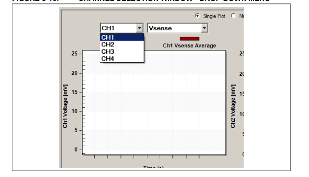
For the Single Plot option, each plot may be configured to show data from any channel with the channel selection window and drop-down menu on the left side above the plot. Each window may be configured to show any of the results from the selected channel with the results selection drop-down menu. Channel selection and results selection are independent for each window. This is illustrated in Figure 3-10 and Figure 3-11. Note that when selecting values from the drop-down menus, it works best to move the cursor with the mouse and click the desired value, instead of using the scroll button on the mouse.
CHANNEL SELECTION WINDOW - DROP-DOWN MENU
FIGURE 3-10:
DS50002673A-page 24
Page 25
Software GUI Description
RESULTS SELECTION WINDOW - DROP-DOWN MENU
FIGURE 3-11:
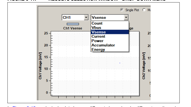
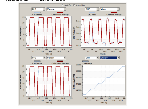
In Figure 3-12, each single plot shows a different channel and a different results register for each channel. Four different results can be displayed for the same channel, the same results for all four channels or any kind of mix and match.
PLOTS WINDOW
FIGURE 3-12:
DS50002673A-page 25
Page 26
3.6.2 Multiple Plots option
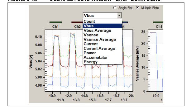
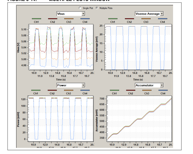
For Multiple Plots option, the same results register from all four channels are always plotted together in each of the four windows. The drop-down menu is used to select which results are plotted in each window, as shown in Figure 3-13. An example of multiple plots is displayed in Figure 3-14.
MULTIPLE PLOTS WINDOW - DROP-DOWN MENU
FIGURE 3-13:
MULTIPLE PLOTS WINDOW
FIGURE 3-14:
DS50002673A-page 26
Page 27

PAC1934 EVALUATION BOARD
(ADM00805) USER’S GUIDE
Chapter 4. Hardware Description
4.1 DEFAULT CONNECTIONS, DEMO MODE AND SYSTEM MODE
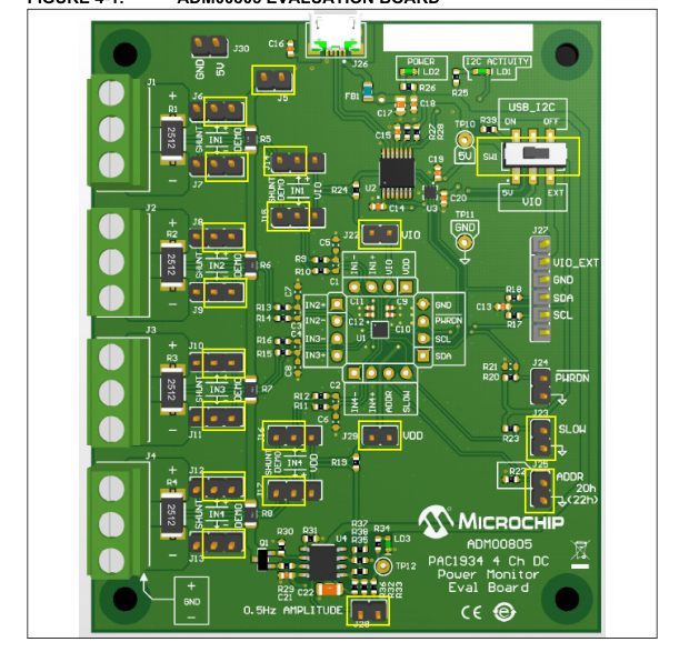
The PAC1934 is placed at the center of the board, in a wafer level chip scale package (WLCSP), U1. It is surrounded by probe points with the pin names labeled. There is a provision for an input filter for each pair on input pins, but these are not populated. The other hardware on the board is described below.
ADM00805 EVALUATION BOARD
FIGURE 4-1:
4.2 DEFAULT CONNECTIONS, DEMO MODE AND SYSTEM MODE FOR
CHANNEL INPUTS
In Figure 4-1, the USB connector is at the top. The yellow rectangles show the default (as shipped) position of the shorting shunts that connect the different pin pairs. There is also a yellow box around SW1. SW1 must be set to the ON position for USB communication to work properly. In this default configuration the inputs of the four chan-
DS50002673A-page 27
Page 28
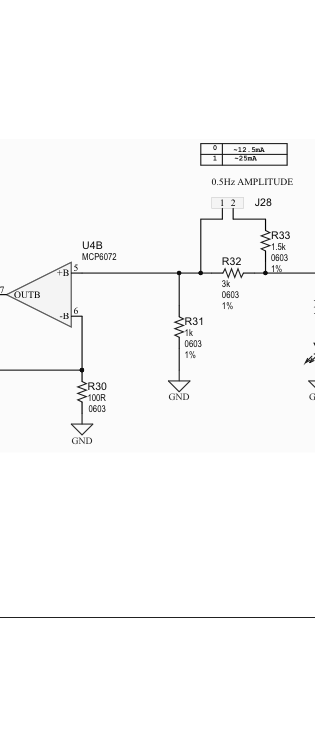
nels are connected across 1Ω sense resistors R5-R8. This is called the DEMO mode configuration. These connections are made by the first column of jumpers on the left side of the board, J6-J13. Each jumper has a shorting shunt connected to the DEMO side of the jumper, near the resistor string R5-R8. These resistors are all in series and connected to the on-board current source that flows through the resistors and then through the shunt on J5 (near the top of the board) to VDD. The shunt on J5 may be removed to disable the on-board current source and see the noise performance of the device with zero input. This current source generates a 0.5 Hz current square wave.
The amplitude is approximately 12.5 mA (J28 open) or 25 mA (J28 shorted, default position). J28 is near the bottom of the board. All of the plots in Chapter 3. “Software GUI Description” are made in DEMO mode with the default connections.
4.3 VBUS AND VSENSE CONNECTIONS - USING EXTERNAL SOURCES FOR
SYTSTEM MODE
To use external sources for VBUS with an external load, the shunts J6 - J13 are moved to the left (shunt position). In this configuration, connect VBUS sources to terminal 1 (top) of the screw terminal connectors J1-J4 and connect the loads to terminal 3 (bottom) of these connectors. The center terminal of each connector is connected to ground for a convenient return connection for the load. Each PAC1934 channel now has an on-board current sense resistor of 4 mΩ connected between the positive (+) input and negative (-) input pins, which gives 25A for the full scale current (VSENSE FSR is fixed at 100 mV). For options that use a different value for RSENSE than the default 1Ω, use the Settings
menu in the GUI to enter the correct sense resistor values so that ISENSE and Power can be properly calculated (see Section 3.2 “Top Menu”). The 4 mΩ resistors (R1-R4) can be unsoldered and replaced with a different value at the discretion of the user. The 4 mΩ resistors have very wide metal connecting each end to terminals 1 and 3 of the connector block, and it is challenging to remove them cleanly. If they are removed, they will reveal a layout that facilitates soldering this wide metal connection to each end of the new sense resistor and a kelvin connection for each end that goes to the inputs of the PAC1934. Both the wide metal to the connector block and the kelvin connection need to be soldered to the new sense resistor.
4.4 OTHER HARDWARE ON THE BOARD
The second columns of jumpers (J14-J17) are by default in the correct position for either DEMO mode or System (shunt) mode. Their function is to enable measurement of the current going into the VDD pin and the current going into the VDD_IO pin. This is described in Section 4.7 “PAC1934 current measurements using the PAC1934.” In the lower right corner are shorted jumpers J23 and J25 to connect the SLOW pin and the ADDRSELECT pin to ground. Grounding the SLOW pin causes the PAC1934 to function at the sample rate programmed by the GUI (default is 1024 samples per second). Removing the shunt on J23 allows the SLOW pin to be pulled high, overriding the programmed sample rate and setting the sampling rate to eight samples/second. The
ADDRSELECT pin sets the SMBus/I2C address to 20h when grounded. Removing the shunt sets the address to 22h. Other addresses can be selected by removing the shunt and changing the value of R22 (see the PAC1934 Data Sheet for values). Nearby is J24 for connecting the PWRDWN to ground if desired.
DS50002673A-page 28
Page 29
Hardware Description
4.5 HARDWARE FOR I2C/SMBUS COMMUNICATION OVER USB OR EXTERNAL
I2C CONNECTION
Directly above J22 is U2. This is an MCP2221 USB-2 to I2C bridge chip that translates the USB communications into I2C read/write commands to configure the PAC1934 and to capture status and results data. To the left of U2 is U3, a level shifter that matches the I2C signals from the MCP2221 to the VIO voltage that the user is using for the PAC1934 VDD_IO. On the far right side of the board, there is a switch SW1 and a connector J27. These are both used when connecting an external I2C connection directly to the board instead of using the USB connection. J27 allows the user to connect the external VIO, SCA, and SCL signals directly to the PAC1934. SW1 disables the USB
bridge and level shifter and connects the pull-up resistors on SCA and SCL pins to the external VIO voltage.
4.6 SIGNAL DESCRIPTION IN DEMO MODE
In DEMO mode, all four channels measure the same ISENSE. VSENSE matching is limited by resistor matching. All four channels measure similar VBUS levels. The VSENSE signals are equal to the current source value multiplied by 1Ω (25/50 mV).The VBUS signal for Channel 1 is +5V USB. The VSENSE inputs for the other channels are separated from +5V USB by each sense resistor’s voltage drop so they are offset from each other. Also, the +5V USB is not a low impedance power supply (it is generated from the USB connection on the PC), so there is a small square wave on each VBUS signal as the ISENSE current interacts with the output impedance of +5V USB. All of the plots in the GUI description above are made in the default DEMO mode
configuration.
4.7 PAC1934 CURRENT MEASUREMENTS USING THE PAC1934.
The ADM00805 Evaluation Board can be used to measure the PAC1934 VDD and VIO currents. For both measurements below, the sense resistor values for Channel 1 (VIO) and/or Channel 4 (VDD) require changing to 10Ω for proper scaling of the ISENSE and power measurements. To measure the current in the VDD_IO pin, move the shunts on J14 and J15 to the VIO position (see Figure 4-1). This connects Channel 1's inputs across R24, which is connected between VDD_IO and VIO. R24 is a 10Ω sense resistor that can measure the current going into the VDD_IO pin on the PAC1934. This is a very low current, and allows the user to see the benefit of using VSENSE average for making very accurate
VSENSE/ISENSE measurements for low currents. The VSENSE measurements have a periodic variation, repeating every four measurements. This periodic variation is due to a design feature that caused the average VSENSE/ISENSE measurement (and the accumulated power) to have nearly zero offset. Figure 4-2 displays VBUS (VDD_IO) and current into VDD_IO.
DS50002673A-page 29
Page 30
MEASURING THE VOLTAGE AND CURRENT ON THE VIO PIN
FIGURE 4-2:
WITH CHANNEL 1
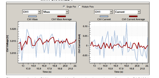
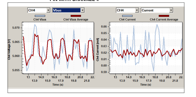
Please note that the GUI is not capable of capturing data points as fast as the PAC1934 is capable of producing them. For this reason, the fastest rate that data can be captured and plotted is approximately one point per 250 samples when sampling at 1024 samples/second. Therefore, the true period variation of the un-averaged measurements cannot be accurately seen with this GUI and appears more like noise. A similar option is available in DEMO mode for measuring the VDD current required by the PAC1934. The IDD current flows in R19 (10Ω). Move the shunts for J16 and J16 to the VDD position to connect Channel 4 inputs across R19, and the GUI may be used to
display IDD as ISENSE on channel 4. In Figure 4-3 VDD is displayed as VBUS with channel 4 and IDD is displayed as Current on Channel 4.
MEASURING THE VOLTAGE AND CURRENT ON THE VDD
FIGURE 4-3:
PIN WITH CHANNEL 4
4.8 ADDITIONAL HARDWARE DETAILS
Directly above and below the PAC1934 are shorted jumpers labeled VIO (J22) and VDD (J29). These provide a place for removing the short and inserting a current meter if the user wishes to measure the current in the VDD_IO pin and/or the VDD pin.
DS50002673A-page 30
Page 31
Hardware Description
J30 may be used to provide external power in place of the +5V USB power derived from VBUS if the USB is not connected. J30 is labeled 5V, but external voltages applied to the pin labeled 5V may be anywhere from 5.5V to 2.7V. This may be needed if the external I2C signals are used with no USB connection J25 sets the I2C/SMBus address to 20h when the shunt is in place. Removing the shunt on J25 changes the address to 22h. Replacing R22 allows selection of other addresses (see the PAC1934 Data Sheet). The shunt on J23 pulls the SLOW pin to ground, so the device is operating at the programmed sample rate. Removing this shunt selects an 8 Hz sample rate for low power
operation. The PAC1934 has a unique feature in that the status of this pin is tracked in a register bit. This allows the GUI to change the displayed sample rate to 8 Hz when the SLOW pin goes high. This is useful in real applications as well, when the user goes to a SLOW sample rate and wants to capture the energy usage before and after the SLOW pin transition. Requirements like this can also benefit from the features described for the SLOW register settings, where the device can automatically be refreshed by a SLOW pin transition.
4.9 DIRECT EXTERNAL I2C CONNECTION
The ADM00805 can be used with direct I2C control from a PC running Windows®, Linux® or other digital controller. VDD_IO may need a different voltage for external I2C use than the default settings for USB control. This is easily implemented by moving SW1 from the ON/5V position used for USB control to the OFF/EXT position used for external I2C control. Connect the external SCA and SCL signals is then required, along with the power (VIO) and ground used for these I2C signals, to J27. Generally, the user will not be able to use the PAC193x Demo Application with direct I2C connection. For Windows® 10 systems, the user can embed sense resistors in series with the
power rails to be monitored/measured, interface to the ADM00805 with direct I2C connections and use the Windows® 10 driver to interface the energy metering functions with the OS.
4.10 JUMPER CONNECTIONS - DEFAULT CONFIGURATION AND OTHER
INFORMATION TABULATED
Table 4-1 shows the default configuration for the shunts on the board to achieve the functionality described in the Section 1.1 “Introduction”. Using this table with the schematic will give a good understanding of the default configuration. In the DEMO mode and SYSTEM/SHUNT mode columns of Table 4-1, a dash (—) means that no jumper is installed or that there is no information needed in this cell. Numbers 12 and 23 mean that the jumper is installed either between the pins 1 and 2 (12) or between the pins 2 and 3 (23).
TABLE 4-1: DEFAULT SHUNT CONNECTIONS
| Jumper no. | DEMO mode | SYSTEM/SHUNT mode | Special connection | Options/Info |
| 1 | — | — | External source | Channel 1 +input, GND, channel 1 –input |
| 2 | — | — | External source | Channel 2 +input, GND, channel 2 –input |
| 3 | — | — | External source | Channel 3 +input, GND, channel 3 –input |
| 4 | — | — | External source | Channel 4 +input, GND, channel 4 –input |
DS50002673A-page 31
Page 32
TABLE 4-1: DEFAULT SHUNT CONNECTIONS (CONTINUED)
| Jumper no. | DEMO mode | SYSTEM/SHUNT mode | Special connection | Options/Info |
| 5 | 12 | — | Open to disable I SOURCE | Connects current source to +5V through R string |
| 6 | 23 | 12 | — | Connect Channel 1 +input |
| 7 | 23 | 12 | — | Connect Channel 1 –input |
| 8 | 23 | 12 | — | Connect Channel 2 +input |
| 9 | 23 | 12 | — | Connect Channel 2 –input |
| 10 | 23 | 12 | — | Connect Channel 3 +input |
| 11 | 23 | 12 | — | Connect Channel 3 –input |
| 12 | 23 | 12 | — | Connect Channel 4 +input |
| 13 | 23 | 12 | — | Connect Channel 4 –input |
| 14 | 12 | 12 | 23 | Connect V to channel DD_IO 1 +input |
| 15 | 12 | 12 | 23 | Connect I to channel VDD_IO 1 –input |
| 16 | 12 | 12 | 23 | Connect V to channel 1 DD +input |
| 17 | 12 | 12 | 23 | Connect I to channel 1 VDD –input |
| 22 | 12 | 12 | — | Remove to insert current meter if desired |
| 23 | 12 | 12 | — | Remove short to enter SLOW mode |
| 24 | Open | Open | — | Short pins 1,2 to enter Power Down state |
| 25 | 12 | 12 | — | Remove shut for address 22h |
| 27 | Open | Open | — | Connect external V , SCA, IO SCL, GND |
| 28 | 12 | 12 | — | Open to boost current source to 25 mA |
| 29 | 12 | 12 | — | Remove to insert current meter if desired |
| 30 | Open | Open | — | Measure +5 USB or connect external 5V |
Note: Switch SW1 is shipped in the ON position. It is easy for this switched to be accidentally moved to a different position when connecting the board. Please confirm that the switch is ON for USB communication, or OFF for external I2C communication.
DS50002673A-page 32
Page 33

PAC1934 EVALUATION BOARD
(ADM00805) USER’S GUIDE
Appendix A. Schematic and Layouts
A.1 INTRODUCTION
This appendix contains the following schematics and layouts for the ADM00805 Evaluation Board:
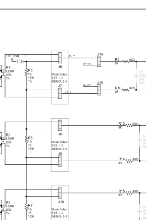
- ADM00805 Evaluation Board - Schematic
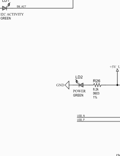
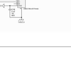
- ADM00805 Evaluation Board - Schematic 2
- ADM00805 Evaluation Board - Schematic 3
- Board - Top Silk
- Board - Top Copper and Silk
- Board - Top Copper
- Board - Bottom Copper
- Board - Bottom Copper and Silk
- Board - Bottom Silk
DS50002673A-page 33
Page 34
4 3 2 1
VDD
SLOW
VDD_IO
ADDR
IN1+
IN4+
IN1-
IN4-
1 2 3 4
DS50002673A-page 34
Page 35
Schematic and Layouts
DS50002673A-page 35
Page 36
DS50002673A-page 36
Page 37
Schematic and Layouts
A.5 BOARD - TOP SILK
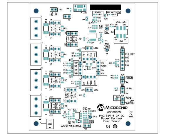
A.6 BOARD - TOP COPPER AND SILK
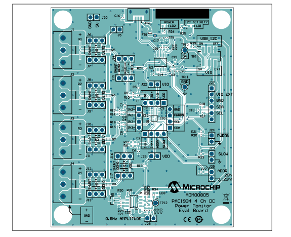
DS50002673A-page 37
Page 38
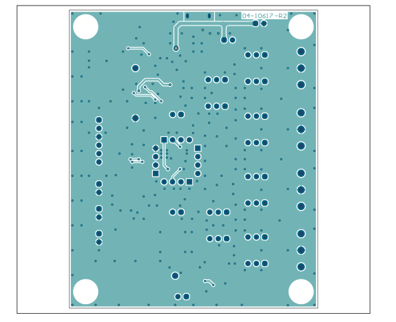
A.7 BOARD - TOP COPPER
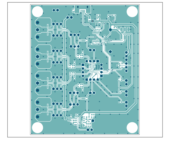
A.8 BOARD - BOTTOM COPPER
DS50002673A-page 38
Page 39
Schematic and Layouts
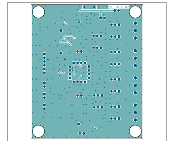
A.9 BOARD - BOTTOM COPPER AND SILK
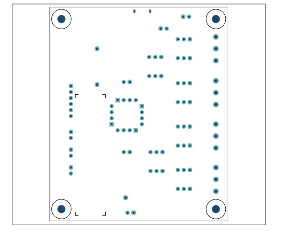
A.10 BOARD - BOTTOM SILK
DS50002673A-page 39
Page 40
NOTES:
DS50002673A-page 40
Page 41

PAC1934
EVALUATION BOARD
(ADM00805) USER’S GUIDE
Appendix B. Bill of Materials (BOM)
TABLE B-1: ADM00805 EVALUATION BOARD - BILL OF MATERIALS (BOM)
| Qty. | Reference | Description | Manufacturer | Part Number |
|---|---|---|---|---|
| 2 | C10, C12 | Capacitor Ceramic, 0.1 μF, 16V, 10% X7R, SMD, 0402 | Murata Electronics North America, Inc. | GRM155R71C104KA88D |
| 7 | C13, C14, C16, C18, C19, C20, C21 | Capacitor Ceramic, 0.1 μF, 16V, 10% X7R, SMD, 0603 | Wurth Elektronik | 885012206046 |
| 1 | C15 | Capacitor Ceramic, 0.47 μF, 6.3V, 10% X5R, SMD, 0603 | Murata Electronics North America, Inc. | GRM188R60J474KA01D |
| 1 | C17 | Capacitor Ceramic, 4.7 μF, 10V, 10% X5R, SMD, 0805 | Panasonic® - ECG | ECJ-GVB1A475M |
| 1 | C22 | Capacitor Ceramic, 2.2 μF, 16V, 10% X7R, SMD, 1206 | Panasonic® - ECG | ECJ-3YB1C225K |
| 2 | C9, C11 | Capacitor Ceramic, 2.2 μF, 10V, 10% X7S, SMD, 0402 | TDK Corporation | C1005X7S1A225K050B C |
| 1 | CBL1 | Mechanical HW Cable USB, Male-A to Male Micro-B, Clear 4 | DongGuan ZhanXin | A006ZX027 |
| 1 | FB1 | Ferrite, 2A, 220R, SMD, 0805 | Murata Electronics North America, Inc. | BLM21PG221SN1D |
| 4 | J1, J2, J3, J4 | Connector Terminal, 5 mm, 1x3 Female, 12-30 AWG, 16A, TH R/A | Wurth Elektronik | 691137710003 |
| 1 | J26 | Connector USB 2.0, Micro-B Female, SMD, R/A | FCI | 10118193-0001LF |
| 1 | J27 | Connector HDR-2.54, Male 1x6, Gold 5.84 MH, TH VERT | FCI | 68001-106HLF |
| 8 | J5, J22, J23, J24, J25, J28, J29, J30 | Connector HDR-2.54, Male 1x2, Gold 5.84 MH, TH VERT | FCI | 77311-118-02LF |
| 12 | J6, J7, J8, J9, J10, J11, J12, J13, J14, J15, J16, J17 | Connector HDR-2.54, Male 1x3, Gold 5.84 MH, TH VERT | FCI | 68000-103HLF |
Note 1: The components listed in this Bill of Materials are representative of the PCB assembly. The released BOM used in manufacturing uses all RoHS-compliant components.
DS50002673A-page 41
Page 42
TABLE B-1: ADM00805 EVALUATION BOARD - BILL OF MATERIALS (BOM) (CONTINUED)
| Qty. | Reference | Description | Manufacturer | Part Number |
|---|---|---|---|---|
| 18 | JP1, JP2, JP3, JP4, JP5, JP6, JP7, JP8, JP9, JP10, JP11, JP12, JP13, JP14, JP15, JP16, JP17, JP18 | Mechanical HW Jumper, 2.54 mm, 1x2 Han- dle, Gold | TE Connectivity, Ltd. | 881545-2 |
| 3 | LD1, LD2, LD3 | Diode LED, Green, 3.2V, 20 mA, 430 mcd, Clear, SMD, 0603 | Wurth Electronik | 150060GS75000 |
| 4 | PAD1, PAD2, PAD3, PAD4 | Mechanical HW Rubber PAD, Cylindrical, D7.9, H5.3, Black | 3M | SJ61A11 |
| 1 | PCB1 | Printed Circuit Board - ADM00805 Evaluation Board | Microchip Technology Inc. | 04-10617-R2 |
| 1 | Q1 | Transistor FET N-CH ZXMN2A01F 20V 1.9A 625 mW SOT-23-3 | Diodes Incorporated® | ZXMN2A01FTA |
| 4 | R1, R2, R3, R4 | Resistor Shunt, MF, 0.004R, 1%, 2W, 2512 | Stackpole Electronics, Inc. | CSNL2512FT4L00 |
| 5 | R17, R18, R27, R28, R39 | Resistor TKF, 4.7k, 1%, 1/10W, SMD, 0603 | Panasonic® - ECG | ERJ-3EKF4701V |
| 2 | R19, R24 | Resistor TKF, 10R, 1%, 1/10W, SMD, 0603 | Panasonic® - ECG | ERJ-3EKF10R0V |
| 3 | R20, R23, R38 | Resistor TKF, 10k, 1%, 1/10W, SMD, 0603 | Panasonic - ECG | ERJ-3EKF1002V |
| 1 | R22 | Resistor TKF, 499R, 1%, 1/10W, SMD, 0603 | Panasonic® - ECG | ERJ-3EKF4990V |
| 3 | R25, R26, R34 | Resistor TKF, 8.2k, 1%, 1/10W, SMD, 0603 | Panasonic - ECG | ERJ-3EKF8201V |
| 1 | R29 | Resistor TKF, 24.9R, 1%, 1/10W, SMD, 0603 | Vishay/Dale | CRCW060324R9FKEA |
| 1 | R30 | Resistor TKF, 100R, 1%, 1/10W, SMD, 0603 | Panasonic® - ECG | ERJ-3EKF1000V |
| 1 | R31 | Resistor TKF, 1k, 1%, 1/10W, SMD, 0603 | Panasonic® - ECG | ERJ-3EKF1001V |
| 1 | R32 | Resistor TKF, 3k, 1%, 1/10W, SMD, 0603 | Panasonic® - ECG | ERJ-3EKF3001V |
| 1 | R33 | Resistor TKF, 1.5k, 1%, 1/10W, SMD, 0603 | Panasonic® - ECG | ERJ-3EKF1501V |
| 1 | R35 | Resistor TKF, 12.1k, 1%, 1/10W, SMD, 0603 | Panasonic® - ECG | ERJ-3EKF1212V |
| 1 | R36 | Resistor TKF, 1M, 5%, 1/10W, SMD, 0603 | Panasonic® - ECG | ERJ-3GEYJ105V |
| 1 | R37 | Resistor TKF, 5.6k, 1%, 1/10W, SMD, 0603 | Yageo Corporation | RC0603FR-075K6L |
| 4 | R5, R6, R7, R8 | Resistor TKF, 1R, 1%, 1/4W, SMD, 1206 | Panasonic® - ECG | ERJ-8RQF1R0V |
| 8 | R9, R10, R11, R12, R13, R14, R15, R16 | Resistor TKF, 0R, 1/10W, SMD, 0603 | Panasonic® - ECG | ERJ-3GSY0R00V |
| 1 | SW1 | Switch Slide DPDT, 6V, 300 mA, JS202011SCQN, SMD | C&K Components | JS202011SCQN |
| 1 | U1 | MCHP Analog Power Current Sense Monitor PAC1934-I/J6CX WLCSP-16 | Microchip Technology Inc. | PAC1934-I/J6CX |
| 1 | U2 | I2C, MCHP Interface USB, UART MCP2221A-I/ST TSSOP-14 | Microchip Technology Inc. | MCP2221A-I/ST |
Note 1: The components listed in this Bill of Materials are representative of the PCB assembly. The released BOM used in manufacturing uses all RoHS-compliant components.
DS50002673A-page 42
Page 43
Bill of Materials (BOM)
TABLE B-1: ADM00805 EVALUATION BOARD - BILL OF MATERIALS (BOM) (CONTINUED)
| Qty. | Reference | Description | Manufacturer | Part Number |
|---|---|---|---|---|
| 1 | U3 | IC Interface, FXMA2102L8X, 2-Bit Voltage, Translator/Buffer Micropak-8 | Fairchild Semiconductor® | FXMA2102L8X |
| 1 | U4 | MCHP Analog OPAMP, 2-Ch, 1.2 MHz, MCP6072-E/SN SOIC-8 | Microchip Technology Inc. | MCP6072-E/SN |
Note 1: The components listed in this Bill of Materials are representative of the PCB assembly. The released BOM used in manufacturing uses all RoHS-compliant components.
TABLE B-2: DO NOT POPULATE
| Qty. | Reference | Description | Manufacturer | Part Number |
|---|---|---|---|---|
| 0 | C1, C2, C3, C4, C5, C6, C7, C8 | Capacitor Ceramic, 10000 pF, 50V, 20% X7R, SMD, 0603 | AVX Corporation | 06035C103KAT2A |
| 0 | R21 | Resistor TKF, 10k 1% 1/10W, SMD, 0603 | Panasonic® - ECG | ERJ-3EKF1002V |
| 0 | TP10 | Misc, Test Point, Multi-purpose, Mini, Red | Keystone Electronics Corp. | 5000 |
| 0 | TP11 | Misc, Test Point, Multi-purpose, Mini, Black | Keystone Electronics Corp. | 5001 |
| 0 | TP12 | Misc, Test Point, Multi-purpose, Mini, White | Keystone Electronics Corp. | 5002 |
| 0 | J18, J19, J20, J21 | CON HDR-2.54 Female 1x4 Gold TH VERT | Samtec, Inc. | SSW-104-01-G-S |
Note 1: The components listed in this Bill of Materials are representative of the PCB assembly. The released BOM used in manufacturing uses all RoHS-compliant components.
DS50002673A-page 43
Page 44
NOTES:
DS50002673A-page 44
Page 45

Worldwide Sales and Service
AMERICAS
ASIA/PACIFIC
ASIA/PACIFIC
Corporate Office
Asia Pacific Office
China - Xiamen
2355 West Chandler Blvd.
Suites 3707-14, 37th Floor
Tel: 86-592-2388138
Chandler, AZ 85224-6199
Tower 6, The Gateway
Fax: 86-592-2388130
Tel: 480-792-7200
Harbour City, Kowloon
China - Zhuhai
Fax: 480-792-7277
Tel: 86-756-3210040
Hong Kong
Technical Support:
Fax: 86-756-3210049
Tel: 852-2943-5100
http://www.microchip.com/
Fax: 852-2401-3431
India - Bangalore
support
Tel: 91-80-3090-4444
Australia - Sydney
Web Address:
Fax: 91-80-3090-4123
Tel: 61-2-9868-6733
www.microchip.com
Fax: 61-2-9868-6755
India - New Delhi
Atlanta
Tel: 91-11-4160-8631
China - Beijing
Duluth, GA
Fax: 91-11-4160-8632
Tel: 86-10-8569-7000
Tel: 678-957-9614
Fax: 86-10-8528-2104
India - Pune
Fax: 678-957-1455
Tel: 91-20-3019-1500
China - Chengdu
Austin, TX
Tel: 86-28-8665-5511
Japan - Osaka
Tel: 512-257-3370
Fax: 86-28-8665-7889
Tel: 81-6-6152-7160
Boston
Fax: 81-6-6152-9310
China - Chongqing
Westborough, MA
Tel: 86-23-8980-9588
Japan - Tokyo
Tel: 774-760-0087
Fax: 86-23-8980-9500
Tel: 81-3-6880- 3770
Fax: 774-760-0088
Fax: 81-3-6880-3771
China - Dongguan
Chicago
Tel: 86-769-8702-9880
Korea - Daegu
Itasca, IL
Tel: 82-53-744-4301
China - Guangzhou
Tel: 630-285-0071
Fax: 82-53-744-4302
Tel: 86-20-8755-8029
Fax: 630-285-0075
Korea - Seoul
China - Hangzhou
Dallas
Tel: 82-2-554-7200
Tel: 86-571-8792-8115
Addison, TX
Fax: 82-2-558-5932 or
Fax: 86-571-8792-8116
Tel: 972-818-7423
82-2-558-5934
China - Hong Kong SAR
Fax: 972-818-2924
Tel: 852-2943-5100
Malaysia - Kuala Lumpur
Detroit
Tel: 60-3-6201-9857
Fax: 852-2401-3431
Novi, MI
Fax: 60-3-6201-9859
China - Nanjing
Tel: 248-848-4000
Tel: 86-25-8473-2460
Malaysia - Penang
Houston, TX
Tel: 60-4-227-8870
Fax: 86-25-8473-2470
Tel: 281-894-5983
Fax: 60-4-227-4068
China - Qingdao
Indianapolis
Tel: 86-532-8502-7355
Philippines - Manila
Noblesville, IN
Tel: 63-2-634-9065
Fax: 86-532-8502-7205
Tel: 317-773-8323
Fax: 63-2-634-9069
China - Shanghai
Fax: 317-773-5453
Tel: 86-21-3326-8000
Singapore
Tel: 317-536-2380
Tel: 65-6334-8870
Fax: 86-21-3326-8021
Los Angeles
Fax: 65-6334-8850
China - Shenyang
Mission Viejo, CA
Tel: 86-24-2334-2829
Taiwan - Hsin Chu
Tel: 949-462-9523
Tel: 886-3-5778-366
Fax: 86-24-2334-2393
Fax: 949-462-9608
Fax: 886-3-5770-955
Tel: 951-273-7800
China - Shenzhen Tel: 86-755-8864-2200
Taiwan - Kaohsiung
Raleigh, NC
Tel: 886-7-213-7830
Fax: 86-755-8203-1760
Tel: 919-844-7510
Taiwan - Taipei
China - Wuhan
New York, NY
Tel: 886-2-2508-8600
Tel: 86-27-5980-5300
Tel: 631-435-6000
Fax: 886-2-2508-0102
Fax: 86-27-5980-5118
San Jose, CA
Thailand - Bangkok
China - Xian
Tel: 408-735-9110
Tel: 66-2-694-1351
Tel: 86-29-8833-7252
Tel: 408-436-4270
Fax: 66-2-694-1350
Fax: 86-29-8833-7256
Canada - Toronto Tel: 905-695-1980 Fax: 905-695-2078
DS50002673A-page 45
EUROPE
Austria - Wels Tel: 43-7242-2244-39 Fax: 43-7242-2244-393 Denmark - Copenhagen Tel: 45-4450-2828 Fax: 45-4485-2829 Finland - Espoo Tel: 358-9-4520-820 France - Paris Tel: 33-1-69-53-63-20 Fax: 33-1-69-30-90-79 France - Saint Cloud Tel: 33-1-30-60-70-00 Germany - Garching Tel: 49-8931-9700 Germany - Haan Tel: 49-2129-3766400 Germany - Heilbronn Tel: 49-7131-67-3636 Germany - Karlsruhe Tel: 49-721-625370 Germany - Munich Tel: 49-89-627-144-0 Fax: 49-89-627-144-44 Germany - Rosenheim Tel: 49-8031-354-560 Israel - Ra’anana Tel: 972-9-744-7705 Italy - Milan Tel: 39-0331-742611 Fax: 39-0331-466781 Italy - Padova Tel: 39-049-7625286 Netherlands - Drunen Tel: 31-416-690399 Fax: 31-416-690340
Norway - Trondheim Tel: 47-7289-7561 Poland - Warsaw Tel: 48-22-3325737 Romania - Bucharest Tel: 40-21-407-87-50 Spain - Madrid Tel: 34-91-708-08-90 Fax: 34-91-708-08-91 Sweden - Gothenberg Tel: 46-31-704-60-40 Sweden - Stockholm Tel: 46-8-5090-4654 UK - Wokingham Tel: 44-118-921-5800 Fax: 44-118-921-5820
11/07/16