
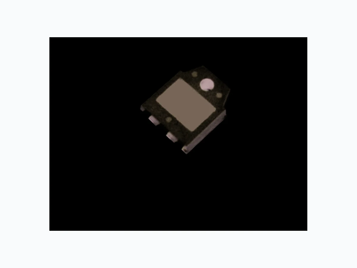
75N10 NELLSEMI
Document overview
- Manufacturer or author: Provided By www.digicamel.com(FREE DATASHEET DOWNLOAD SITE)
- PDF pages: 8
Technical content
www.nellsemi.com Page 1 of 8 TO-3PB G D S D N-Channel Power MOSFET (75A, 100Volts)
DESCRIPTION
Low reverse transfer capacitance (C = 275pF typical)RSS R = 0.025Ω @ V = 10V DS(ON) GS Ultra low gate charge(74nC typical) Fast switching capability 100% avalanche energy specified Improved dv/dt capability 150°C operation temperature
FEATURES
I (A)D 75 V (V)DSS 100 0.025 @ V = 10VGS R (Ω)DS(ON) Q (nC) typicalG UNIT V /ns V A mJ °C/W ºC -55 to 150 VALUE 100 ±20 200 100 1.90 ABSOLUTE MAXIMUM RATINGS (T = 25°C unless otherwise specified)C T =25°C to 150°CJ TEST CONDITIONS R =1MΩGS T =25°C C T =100°C C Operation junction temperature Storage temperature Peak diode recovery dv/dt(Note 4) PARAMETER Pulsed Drain current(Note 1) Continuous Drain Current Total power dissipation Gate to Source voltage Drain to Gate voltage Drain to Source voltage SYMBOL VDGR VDSS dv/dt VGS IDM TSTG PD ID TJ TL . .lbf in (N m) 300Maximum soldering temperature, for 10 seconds Mounting torque, #6-32 or M3 screw -55 to 150 Note: 1. Caluclated continuous current based on maximum allowable junction temperature. Package limitation current is 75A 10 (1.1) 1.6mm from case IAR Avalanche current(Note 1) 50 2.Repetitive rating: pulse width limited by junction temperature. 1000Single pulse avalanche energy(Note 3)EAS 3.L = 0.8mH, I ≤ 50A , R = 25 ,T °C.AS G J Ω ≤ 150 Linear derating factor above T =25°C C 30Repetitive avalanche energy(Note 1)EAR l =50A, =0.8mHAS L W They are designed as an extremely efficient and reliable device for use in a wide variety of applications. These transistors can be operated directly from The Nell 75N10 is a three-terminal silicon device with current conduction capability of 75A, fast switching speed, low on-state resistance, breakdown voltage rating of 100V, and max. threshold voltage of 5 volts. (75N10A) D (Drain) G (Gate) S (Source) 300T =25°C C TO-220AB (75N10B) D GDS integrated circuits. I (A), Package LimitedD 75 4.I ≤ 50A, di/dt ≤ 100A/µs, V ≤ V , T °C.SD DD (BR)DSS J = 150
UNITMin. 0.42 THERMAL RESISTANCE PARAMETER Thermal resistance, junction to case SYMBOL Rth(j-c) Typ. Max. ºC/W Thermal resistance, junction to ambientRth(j-a) UNIT V ns μA pF nC Max. 250 100 -100 100 0.105 2250 275 890 ELECTRICAL CHARACTERISTICS (T = 25°C unless otherwise specified)C V = 0V, I = 250µAGS D TEST CONDITIONS I = 1mA, referenced to 25°CD V =100V, V =0V DS GS T = 25°C C Fall time Gate to source reverse leakage current Input capacitance Total gate charge Output capacitance PARAMETER Rise time Gate to source forward leakage current Turn-on delay time Reverse transfer capacitance Breakdown voltage temperature coefficient Drain to source breakdown voltage Turn-off delay time SYMBOL CISS ▲ ▲V /(BR)DSS TJ V(BR)DSS IGSS QG tr tf QGS 18Gate to source charge V = 50V, V = 10V, I = 37.5A DS GS D Drain to source leakage currentIDSS COSS CRSS td(ON) td(OFF) V/ºC mΩ S nA T =125°C C Typ.Min. V = 50V, DD (Note 1) I = 75A,R = 10Ω,D G V = 10VGS V = 25V, V = 0V, f =1MHzDS GS V = -20V, V = 0VGS DS V = 20V, V = 0VGS DS V =10V, I =37.5A DS DForward transconductance Static drain to source on-state resistanceRDS(ON) gfS V = 10V, l = 37.5A (Note 1)GS D Gate to drain charge (Miller charge)QGD 40 V =80V, V =0V DS GS 2.5 V5.0V =V , I =250μA GS DS DGate threshold voltageVGS(TH) 75N10 Series TO-220AB TO-3PB μHBetween lead, 6mm from package and center of die 7.5Internal source inductanceLS Internal drain inductanceLD 4.5 OFF CHARACTERISTICS ON CHARACTERISTICS DYNAMIC CHARACTERISTICS SWITCHING CHARACTERISTICS www.nellsemi.com Page 2 of 8
SOURCE TO DRAIN DIODE RATINGS AND CHARACTERISTICS (T = 25°C unless otherwise specified)C UNITMax.TEST CONDITIONSPARAMETERSYMBOL Typ.Min. VI = 75A, V = 0VSD GS Diode forward voltageVSD 1.5 Integral reverse P-N junction diode in the MOSFET Continuous source to drain currentI s(IsD) 75 D (Drain) G (Gate) S (Source) A Pulsed source currentISM 200 I = 75A, V = 0V, SD GS dI /dt = 100A/µs F Reverse recovery timetrr ns120 μCReverse recovery chargeQrr 1.4 Note: 1. Pulse test: Pulse width ≤ 400μs, duty cycle ≤ 2%. tON Forward turn-on time Intrinsic turn-on time is negligible (turn-on is domonated by LS+LD) SEMICONDUCTOR RoHS RoHS Nell High Power Products 75N10 Series ORDERING INFORMATION SCHEME MOSFET series Current rating, ID Voltage rating, VDS 75 = 75A 10 = 100V
75 N 10 A
N = N-Channel A = TO-220AB B = TO-3PB www.nellsemi.com Page 3 of 8
Fig.1 Output characteristics Fig.4 R Normalized to 0.5 l value vs.DS(on) D Junction temperature Drain current, l (A) D R (DS(on) Normalized) Junction temperature, T (°C)J Fig.3 Output characteristics Fig.2 Extended output characteristics Drain-source Voltage, V (V) DS Drain current, l (A) D Drain-source Voltage, V (V) DS Drain current, l (A) D Drain-source Voltage, V (V) DS V = 10VGS 9V T = 25°CJ 120 110 0 1 2 3 4 5 6 7 8 9 10 11 12 100 T = 25°CJ V = 10VGS T = 125°CJ V = 10VGS 2.2 1.8 1.6 1.4 1.2 0.8 0.6 -50 -25 0 25 50 75 100 125 150 V = 10VGS l = 75AD l = 37.5AD R (Normalized)DS(on) Drain current, l (A)D Fig.5 R Normalized to 0.5 l value vs.DS(on) D Drain current Fig.6 Maximum drain current vs. Case temperature Case temperature, T C (°C) 2.0 2.8 2.6 2.4 2.2 1.8 1.6 1.4 1.2 1.0 0.8 0 20 40 60 -50 -25 25 50 75 100 125 1500 Drain current, l (A) D 80 100 120 V = 10VGS T = 125°CJ T = 25 °CJ www.nellsemi.com Page 4 of 8
Fig.7 Typical transfer characteristics Fig.8 Forward transconductance Fig.9 Typical source to drain diode forward voltage Fig.10 Gate charge characteristics Gate-Source voltage, V (V)GS Gate charge, Q (nC)G Gate-Source voltage, V (V) GS Forward transconductance, g (S) fs Drain current, l (A)D 0 20 40 60 Source-drain current, l (A) S Diode forward voltage, V (V)SD 0 10 20 30 40 50 60 70 80 Drain current, l (A) D 120 105 5 6 7 8 9 10 11 T = 125°CJ 25°C -40°C 80 100 120 140 160 180 25°C T = 125°CJ -40°C 200 180 160 140 120 100 1.7 T = 125°CJ T = 25°CJ V =50VDS l =37.5AD l =10mAG Fig.11 Typical capacitance vs. drain-Source voltage Fig.12 Maximum safe operating area 10000 1000 100 0 5 10 15 20 25 30 35 40 1000 100 100 1000101 Drain current, l (A) D Capacitance (pF) Drain-source voltage, V (V) DS Drain-source voltage, V (V) DS f=1 MHZ Ciss Coss Crss R LimitDS(on) T =150°Cj 25µs T =25°CC Single Pulse 100µs 1ms 10ms DC 100 www.nellsemi.com Page 5 of 8
Fig.13 Maximum transient thermal Resistance R (°C/W) th(j-c) Pulse width (S) 0.45 0.40 0.35 0.30 0.25 0.20 0.15 0.10 0.05 -310 Fig.14b. Switching time waveforms VDS VGS 90% 10% td(ON) tR td(OFF) tF Fig.14a. Switching time test circuit RD VDS VGS RG 10V Pulse width ≤ 1µs Duty Factor ≤ 0.1% D.U.T. VDD Fig.15a. Unclamped lnductive test circuit Fig.15b. Unclamped lnductive waveforms A 15V DRIVER VDD D.U.T. VDS RG 20V tP lAS 0.01Ω L VDD tp Time lAS BVDSS lD(t) VDS(t) -210 -110 010 www.nellsemi.com Page 6 of 8
Fig.16b. Gate charge test circuit QG QGS QGD 10V VGS Charge P.W. Period di/dt Diode Recovery dv/dt Ripple ≤ 5% Body Diode Forward Drop Re-Applied Voltage Reverse Recovery Current Body Diode Forward Current VGS=10V VDD ISD Driver Gate Drive D.U.T. I SD Waveform D.U.T. VDS Waveform Inductor Curent D = P.W. Period Circuit Layout Considerations Low Stray lnductance Ground Plane Low Leakage lnductance Current Transformer dv/dt controlled by RG Driver same type as D.U.T. l controlled by Duty Factor DSD " " D.U.T. -Device Under Test D.U.T. RG VDD *V = 5V for Logic Level DevicesGS Current Regulator Same Type as D.U.T. 12V 0.2µF 50KΩ 0.3µF VGS 3mA D.U.T. VDS lDlG Fig.17 Peak diode recovery dv/dt test circuit for N-Channel MOSFET Fig.16a. Basic gate charge waveform Current Sampling Resistors www.nellsemi.com Page 7 of 8
www.nellsemi.com Page 8 of 8 TO-3PB 15.6±0.4 9.6 2.04.0 19.9±0.320.0 min 4.0 max 2 1.05 +0.2 -0.1 5.45±0.1 5.45±0.1 Φ3.2 0,1± 1.8 5.0 .±0 2 4.8±0.2 2.0±0.1 0.65 +0.2 -0.1 1.4 G D S 1 2 3 All dimensions in millimeters(inches) D (Drain) G (Gate) S (Source) All dimensions in millimeters(inches) D (Drain) G (Gate) S (Source) 2.87 (0.113) 2.62 (0.103) 9.40 (0.370) 9.14 (0.360) 10.54 (0.415) MAX. 16.13 (0.635) 15.87 (0.625) PIN 4.06 (0.160) 3.56 (0.140) 1.45 (0.057) 1.14 (0.045) 2.67 (0.105) 2.41 (0.095) 2.65 (0.104) 2.45 (0.096) 5.20 (0.205) 4.95 (0.195) 0.90 (0.035) 0.70 (0.028) 3.91 (0.154) 3.74 (0.148) G S D 4.70 (0.185) 4.44 0.1754 ( ) 1.39 (0.055) 1.14 (0.045) 3.68 (0.145) 3.43 (0.135) 8.89 (0.350) 8.38 (0.330) 29.16 (1.148) 28.40 (1.118) 14.22 (0.560) 13.46 (0.530) 0.56 (0.022) 0.36 (0.014) 2.79 (0.110) 2.54 (0.100) 15.32 (0.603) 14.55 (0.573) TO-220AB