
Single bilateral switch
Document overview
- Manufacturer or author: STMICROELECTRONICS
- PDF pages: 15
Technical content
Features
■ High speed: tPD = 0.3 ns (typ.) at VCC = 5 V tPD = 0.4 ns (typ.) at VCC = 3.3 V ■ Low power dissipation: I CC = 1 μA (max.) at TA =2 5° C ■ Low "ON" resistance: RON =6 . 5Ω (typ.) at VCC = 5 V I I/O = 1 mA RON = 8.5 Ω (typ.) at VCC = 3.3 V II/O = 1 mA ■ Sine wave distortion: 0.04% at VCC = 3 . 3V f = 1k H z ■ Wide operating range: V CC (opr) = 2 V to 5.5 V ■ Improved latch-up immunity
Description
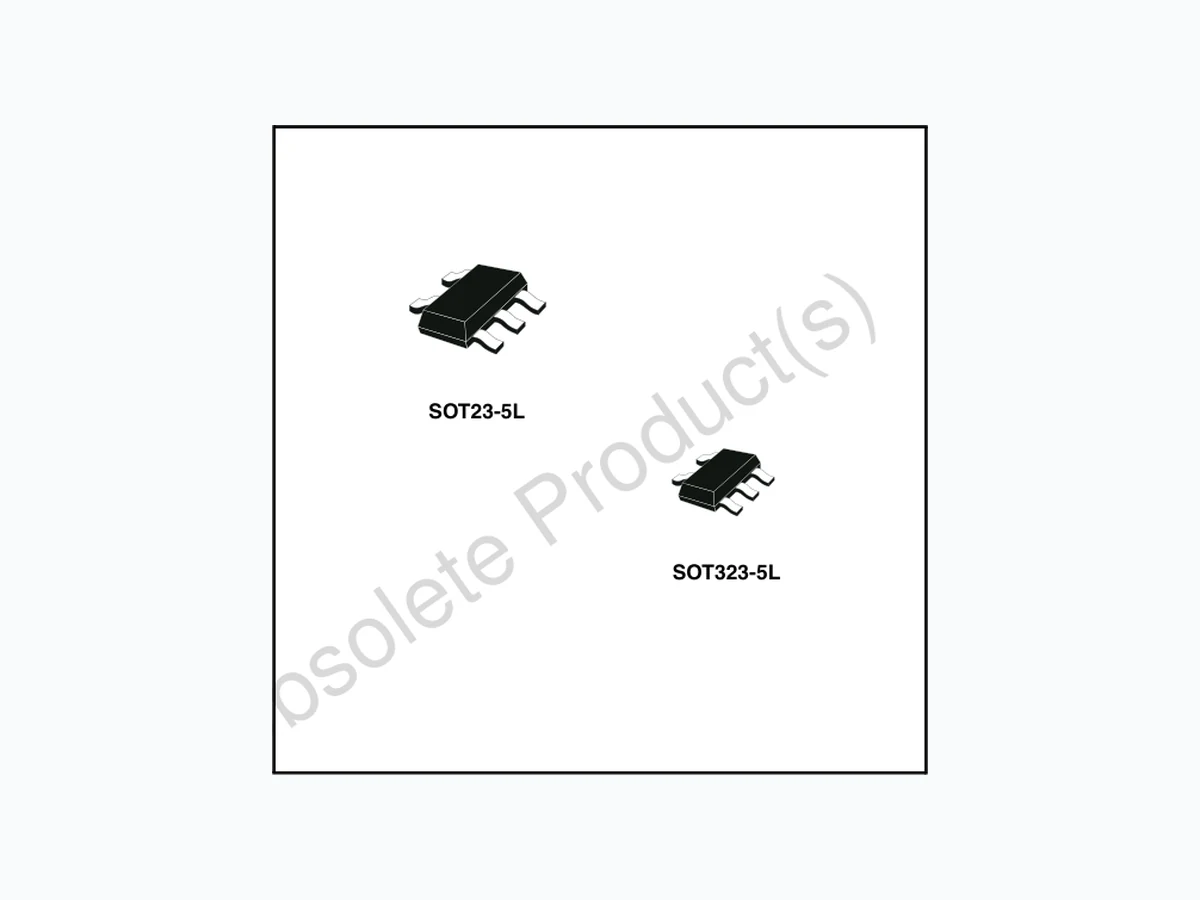
The 74V1G66 is an advanced high-speed CMOS single bilateral switch fabricated in silicon gate C 2MOS technology. It achieves high speed propagation delay and very low ON resistances while maintaining true CMOS low power consumption. This bilateral switch handles rail to rail analog and digital signals that may vary across the full power supply range (from GND to V CC). The C input is provided to control the switch and it is compatible with standard CMOS outputs. The switch is ON (port I/O is connected to port O/I) when the C input is held high and OFF (high impedance state exists between the two ports) when C is held low. It can be used in many applications as battery powered systems or test equipments. The 74V1G66 is available in the commercial and extended temperature range in SOT23-5L and SOT323-5L packages. All inputs and outputs are equipped with protection circuits against static discharge, giving them ESD immunity and transient excess voltage. SOT323-5L SOT23-5L Table 1. Device summary
1 Pin connection
Figure 1. Pin connection and IEC logic symbols Figure 2. Input equivalent circuit Table 2. Pin description
1 I/O Independent input/output
2 O/I Independent output/input
3 GND Ground (0 V)
4 C Enable input (active high)
Table 3. Truth table
2 Maximum rating
extended periods may affect device reliability. Table 4. Absolute maximum ratings Table 5. Recommended operating conditions
- V IN from 30% to 70% of VCC on control pin.
Table 6. DC specifications
- Voltage range is 3.3 V ± 0.3 V.
- Voltage range is 5 V ± 0.5 V.
Table 7. AC electrical characteristics (C L = 50 pF, input tr = tf = 3 ns)
- Voltage range is 3.3 V ± 0.3 V.
- Voltage range is 5 V ± 0.5 V.
Table 8. Capacitive characteristics
- C PD is defined as the value of the IC’s internal equivalent capacitance which is calculated from the operating current
consumption without load. (Refer to the test circuit). Average operating current can be obtained by the following equation. ICC(opr) = CPD x VCC x fIN + ICC.
Table 9. Analog switch characteristics (GND = 0 V; T A = 25°C) 3.3(1) Adjust fIN voltage to obtain 0 dBm at VOS.
- Voltage range is 3.3 V ± 0.3 V
- Voltage range is 5.0 V ± 0.5 V
3 Switching characteristics test circuit
Figure 3. Enable and disable timing (circu it) Figure 4. Enable and disable timing Figure 5. Resistive feedthrough attenuation Fi gure 6. Capacitive feedthrough attenuation Figure 7. Bandwidth attenuation Figure 8. Maximum control frequency
4 Package mechanical data
In order to meet environmental requirements, ST offers these devices in ECOPACK® packages. These packages have a Lead-free second level interconnect. The category of second level interconnect is marked on the package and on the inner box label, in compliance with JEDEC Standard JESD97. The maximum ratings related to soldering conditions are also marked on the inner box label. ECOPACK is an ST trademark. ECOPACK specifications are available at: www.st.com. Obsolete Product(s) - Obsolete Product(s)
Package mechanical data 74V1G66 DIM. mm. mil s A 0.90 1.45 35.4 57.1 A1 0.00 0.10 0.0 3.9 A2 0.90 1. 30 35.4 51.2 b 0.35 0.50 1 3.7 19.7 C 0.09 0.20 3.5 7. 8 D2 . 80 3.00 110.2 11 8.1 E 1.50 1.75 59.0 6 8.8 e0 . 9 5 37.4 H 2.60 3.00 102. 3 118.1 L 0.10 0.60 3.9 2 3.6 SOT23-5L MECHANICAL DATA 7049676C Obsolete Product(s) - Obsolete Product(s)
DIM. mm. mil s A0 . 80 1.10 31.5 4 3.3 A1 0.00 0.10 0.0 3.9 A2 0.80 1.00 31.5 39.4 b 0.15 0. 30 5.9 11. 8 C 0.10 0.1 83 .9 7.1 D1 . 80 2.20 70.9 86.6 E1 . 80 2.40 70.9 94.5 E1 1.15 1. 35 45. 3 53.1 e .65 25.6 e1 1.3 51.2 L 0.10 0. 30 3.9 11. 8 SOT323-5L MECHANICAL DATA Obsolete Product(s) - Obsolete Product(s)
Package mechanical data 74V1G66 DIM. mm. inch A1 807 . 0 86 D 20.2 0.795 N6 0 2 . 362 T 14.4 0.567 Tape & Reel SOT23-xL MECHANICAL DATA Obsolete Product(s) - Obsolete Product(s)
DIM. mm. inch A 175 1 801 856 . 8897 . 0 867 . 2 83 D 20.2 0.795 N 59.5 60 60.5 2. 362 T 14.4 0.567 Ao 2.25 0.0 88 Bo 2.7 0.106 Ko 1.2 0.047 Tape & Reel SOT323-xL MECHANICAL DATA Obsolete Product(s) - Obsolete Product(s)
5 Revision history
Table 10. Document revision history 01-Apr-2004 7 Updated data reel information. 28-Oct-2008 8 Document reformatted to improve readability. Updated Table 6: DC specifications on page 4.