Download PDF
74HC7046A PHILIPS
Document overview
- PDF pages: 38
Technical content
Page 1
Page 2
Page 3
Page 4
| SYMBOL | PARAMETER | CONDITIONS | TYPICAL | UNIT | |
|---|---|---|---|---|---|
| HC | HCT | ||||
| f o | VCO centre frequency | C1 = 40 pF; R1 = 3 kΩ; V = 5 V CC | 19 | 19 | MHz |
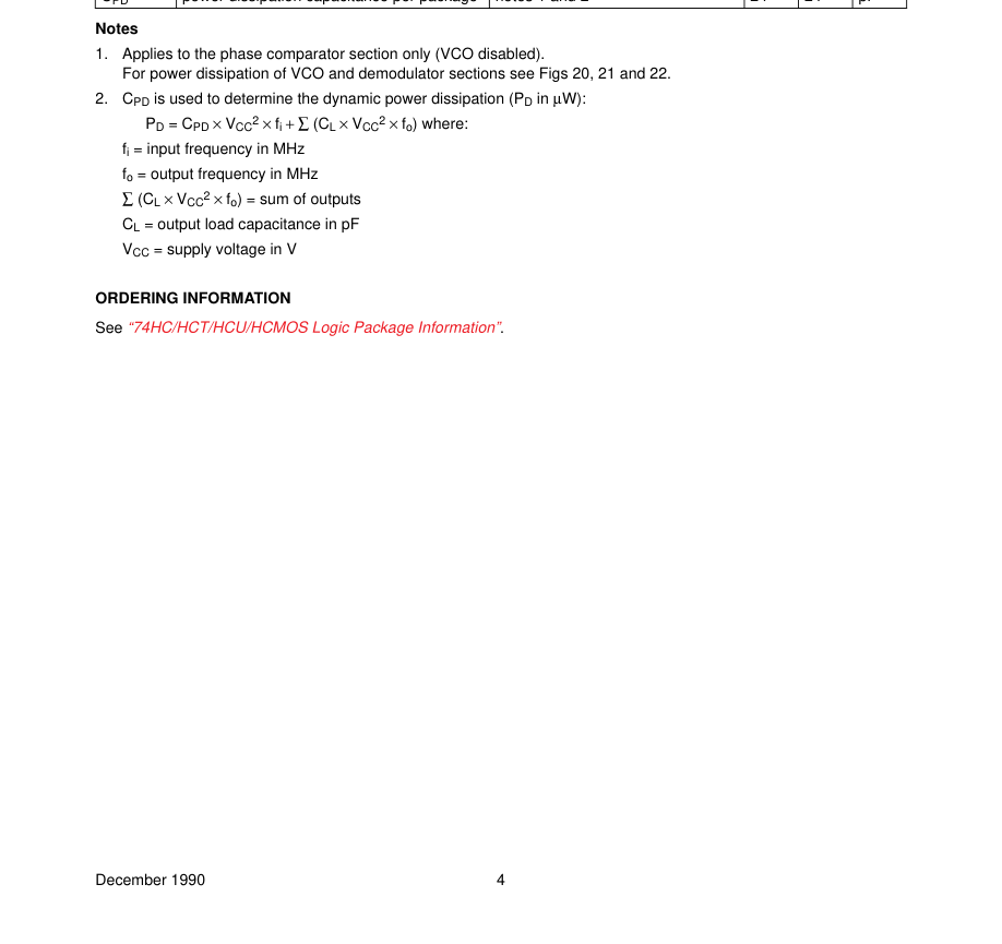
| C I | input capacitance (pin 5) | 3.5 | 3.5 | pF | |
| C PD | power dissipation capacitance per package | notes 1 and 2 | 24 | 24 | pF |
Page 5
Page 6

Page 7
Page 8
Page 9
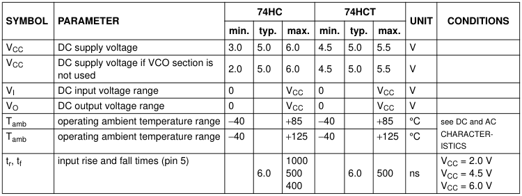

| SYMBOL | PARAMETER | MIN. | MAX. | UNIT | CONDITIONS |
|---|---|---|---|---|---|
| V CC | DC supply voltage | −0.5 | +7 | V | |
| ±I IK | DC input diode current | 20 | mA | for V < −0.5 V or V > V + 0.5 V I I CC | |
| ±I OK | DC output diode current | 20 | mA | for V < −0.5 V or V > V + 0.5 V O O CC | |
| ±I O | DC output source or sink current | 25 | mA | for − 0.5 V < V < V + 0.5 V O CC | |
| ±I ; CC ±I GND | DC V or GND current CC | 50 | mA | ||
| T stg | storage temperature range | −65 | +150 | °C | |
| P tot | power dissipation per package plastic DIL | 750 | mW | for temperature range: −40 to +125 °C 74HC/HCT above +70 °C: derate linearly with 12 mW/K | |
| plastic mini-pack (SO) | 500 | mW | above +70 °C: derate linearly with 8 mW/K |
Page 10
Page 11
Page 12
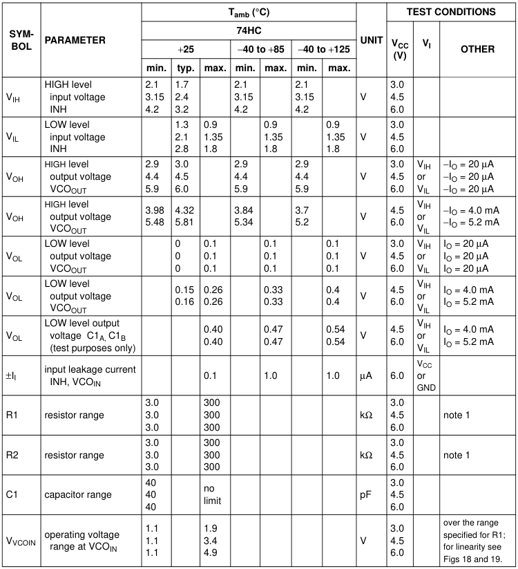

Page 13
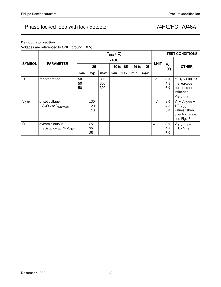
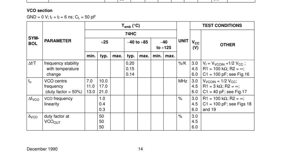
Page 14
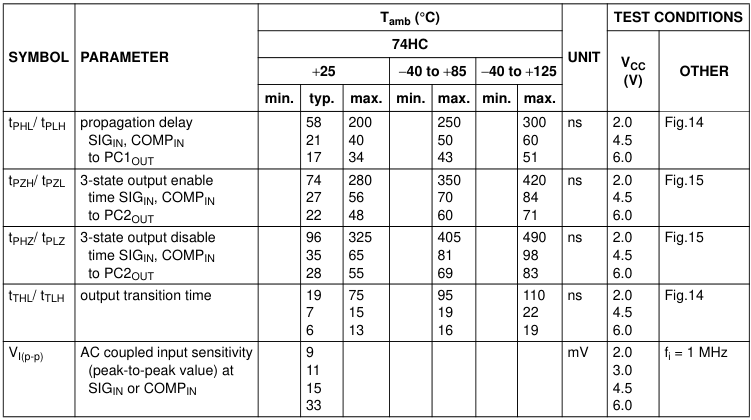
Page 15
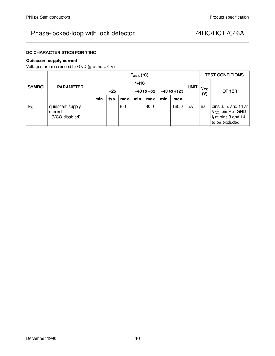
| SYMBOL | PARAMETER | T (°C) amb | UNIT | TEST CONDITIONS | |||||||
|---|---|---|---|---|---|---|---|---|---|---|---|
| 74HCT | V CC (V) | OTHER | |||||||||
| +25 | −40 to +85 | −40 to +125 | |||||||||
| min. | typ. | max. | min. | max. | min. | max. | |||||
| I CC | quiescent supply current (VCO disabled) | 8.0 | 80.0 | 160.0 | µA | 6.0 | pins 3, 5 and 14 at V ; pin 9 at CC GND; I at pins 3 I and 14 to be excluded | ||||
| ∆I CC | additional quiescent supply current per input pin for unit load coefficient is 1 (note 1) V = V −2.1 V I CC | 100 | 360 | 450 | 490 | µA | 4.5 to 5.5 | pins 3 and 14 at V ; pin 9 at CC GND; I at pins 3 I and 14 to be excluded | |||

| INPUT | UNIT LOAD COEFFICIENT |
|---|---|
| INH | 1.00 |
Page 16
| SYM BOL | PARAMETER | T (°C) amb | UNIT | TEST CONDITIONS | ||||||||
|---|---|---|---|---|---|---|---|---|---|---|---|---|
| 74HCT | V CC (V) | V I | OTHER | |||||||||
| +25 | −40 to +85 | −40 to +125 | ||||||||||
| min. | typ. | max | min. | max. | min. | max. | ||||||
| V IH | DC coupled HIGH level input voltage SIG , COMP IN IN | 3.15 | 2.4 | V | 4.5 | |||||||
| V IL | DC coupled LOW level input voltage SIG , COMP IN IN | 2.1 | 1.35 | V | 4.5 | |||||||
| V OH | HIGH level output voltage LD, PC nOUT | 4.4 | 4.5 | 4.4 | 4.4 | V | 4.5 | V IH or V IL | −I = 20 µA O | |||
| V OH | HIGH level output voltage LD, PC nOUT | 3.98 | 4.32 | 3.84 | 3.7 | V | 4.5 | V IH or V IL | −I = 4.0 mA O | |||
| V OL | LOW level output voltage LD, PC nOUT | 0 | 0.1 | 0.1 | 0.1 | V | 4.5 | V IH or V IL | I = 20 µA O | |||
| V OL | LOW level output voltage LD, PC nOUT | 0.15 | 0.26 | 0.33 | 0.4 | V | 4.5 | V IH or V IL | I = 4.0 mA O | |||
| ±I I | input leakage current SIG , COMP IN IN | 30 | 38 | 45 | µA | 5.5 | V CC or GND | |||||
| ±I OZ | 3-state OFF-state current PC2 OUT | 0.5 | 5.0 | 10.0 | µA | 5.5 | V IH or V IL | V = V O CC or GND | ||||
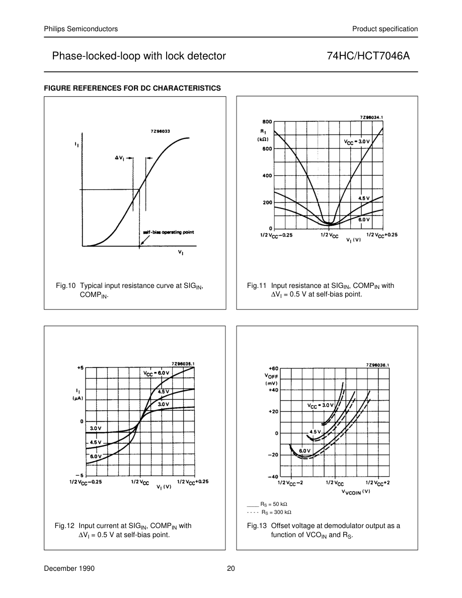
| R I | input resistance SIG , COMP IN IN | 250 | kΩ | 4.5 | V at self-bias I operating point; ∆V = 0.5 V; see Figs I 10, 11 and 12 | |||||||
Page 17
| SYMBOL | PARAMETER | T (°C) amb | UNIT | TEST CONDITIONS | ||||||||
|---|---|---|---|---|---|---|---|---|---|---|---|---|
| 74HCT | V CC (V) | V I | OTHER | |||||||||
| +25 | −40 to +85 | −40 to +125 | ||||||||||
| min. | typ. | max. | min. | max. | min. | max. | ||||||
| V IH | HIGH level input voltage INH | 2.0 | 1.6 | 2.0 | 2.0 | V | 4.5 to 5.5 | |||||
| V IL | LOW level input voltage INH | 1.2 | 0.8 | 0.8 | 0.8 | V | 4.5 to 5.5 | |||||
| V OH | HIGH level output voltage VCO OUT | 4.4 | 4.5 | 4.4 | 4.4 | V | 4.5 | V IH or V IL | −I = 20 µA O | |||
| V OH | HIGH level output voltage VCO OUT | 3.98 | 4.32 | 3.84 | 3.7 | V | 4.5 | V IH or V IL | −I = 4.0 mA O | |||
| V OL | LOW level output voltage VCO OUT | 0 | 0.1 | 0.1 | 0.1 | V | 4.5 | V IH or V IL | I = 20 µA O | |||
| V OL | LOW level output voltage VCO OUT | 0.15 | 0.26 | 0.33 | 0.4 | V | 4.5 | V IH or V IL | I = 4.0 mA O | |||
| V OL | LOW level output voltage C1 , C1 A B (test purposes only) | 0.40 | 0.47 | 0.54 | V | 4.5 | V IH or V IL | I = 4.0 mA O | ||||
| ±I I | input leakage current INH, VCO IN | 0.1 | 1.0 | 1.0 | µA | 5.5 | V CC or GND | |||||
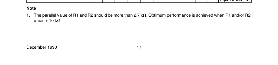
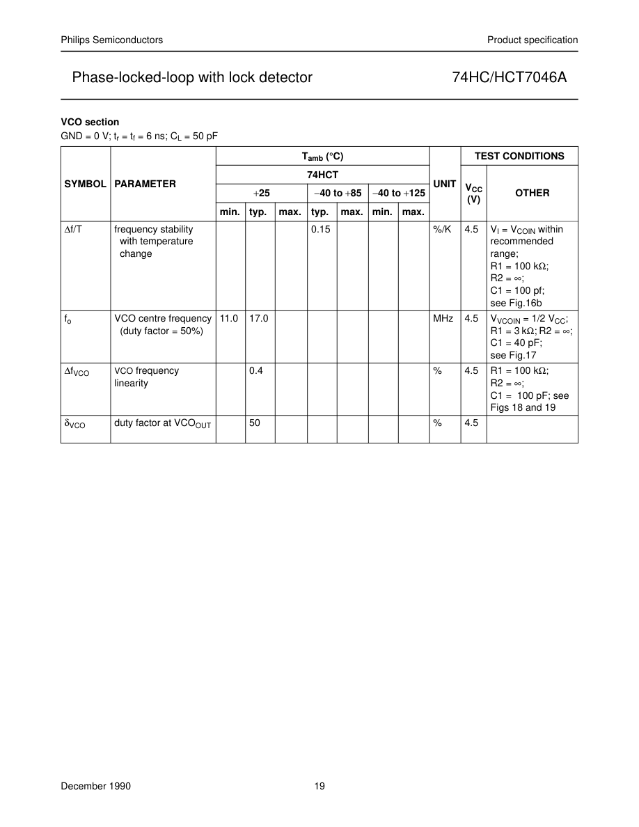
| R1 | resistor range | 3.0 | 300 | kΩ | 4.5 | note 1 | ||||||
| R2 | resistor range | 3.0 | 300 | kΩ | 4.5 | note 1 | ||||||
| C1 | capacitor range | 40 | no limit | pF | 4.5 | |||||||
| V VCOIN | operating voltage range at VCO IN | 1.1 | 3.4 | V | 4.5 | over the range specified for R1; for linearity see Figs 18 and 19. | ||||||
Page 18
| SYMBOL | PARAMETER | T (°C) amb | UNIT | TEST CONDITIONS | |||||||
|---|---|---|---|---|---|---|---|---|---|---|---|
| 74HCT | V CC (V) | OTHER | |||||||||
| +25 | −40 to +85 | −40 to +125 | |||||||||
| min. | typ. | max. | min. | max. | min. | max. | |||||
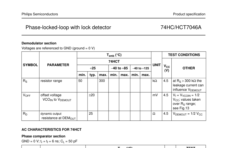
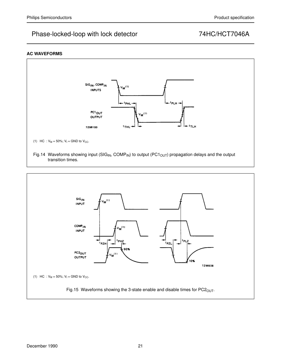
| t / t PHL PLH | propagation delay SIG , COMP IN IN to PC1 OUT | 21 | 40 | 50 | 60 | ns | 4.5 | Fig.14 | |||
| t / t PZH PZL | 3-state output enable time SIG , COMP IN IN to PC2 OUT | 27 | 56 | 70 | 84 | ns | 4.5 | Fig.15 | |||
| t / t PHZ PLZ | 3-state output disable time SIG , COMP IN IN to PC2 OUT | 35 | 65 | 81 | 98 | ns | 4.5 | Fig.15 | |||
| t / t THL TLH | output transition time | 7 | 15 | 19 | 22 | ns | 4.5 | Fig.14 | |||
| V I(p-p) | AC coupled input sensitivity (peak-to-peak value) at SIG or COMP IN IN | 15 | mV | 4.5 | f = i 1 MHz | ||||||
Page 19
Page 20
Page 21
Page 22

Page 23
Page 24
Page 25
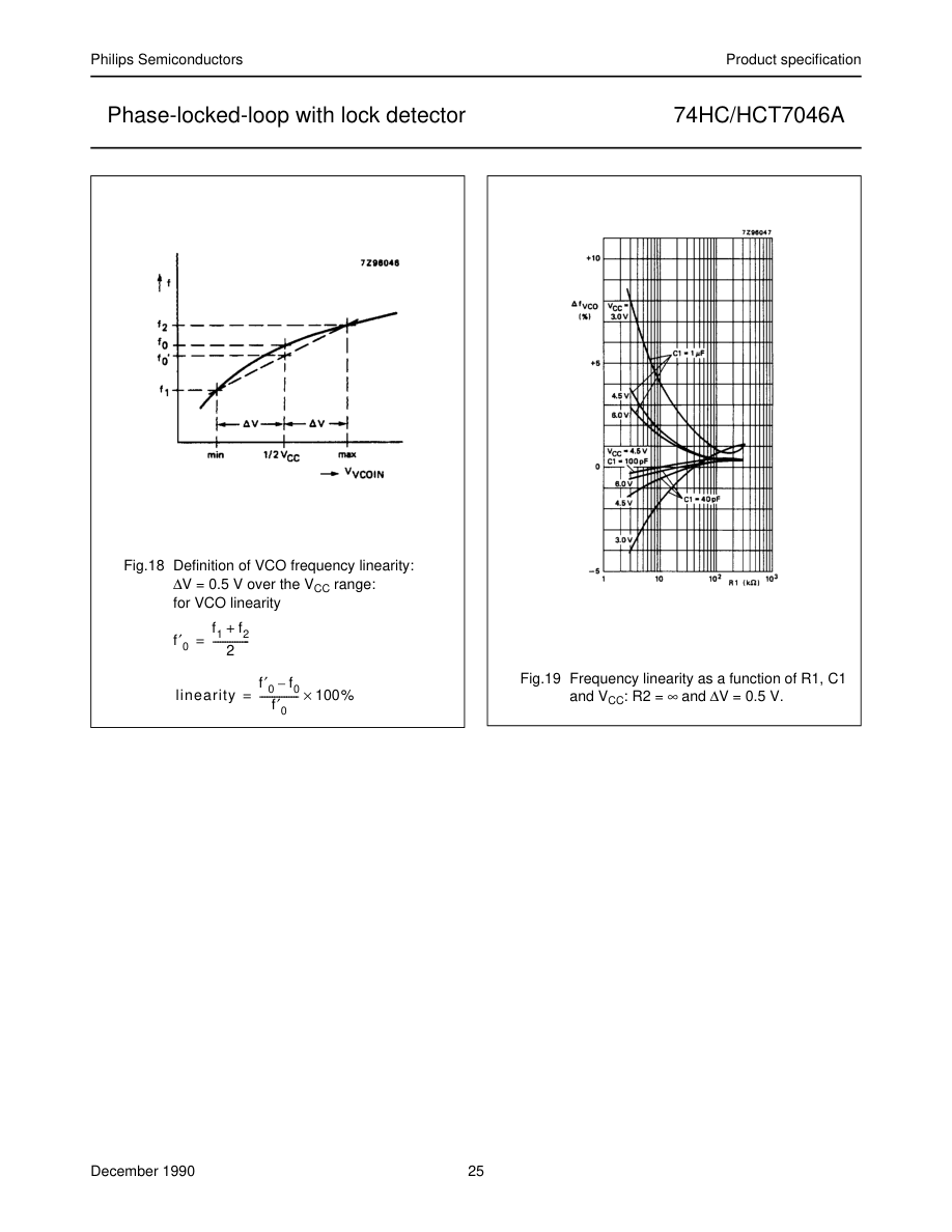
Page 26
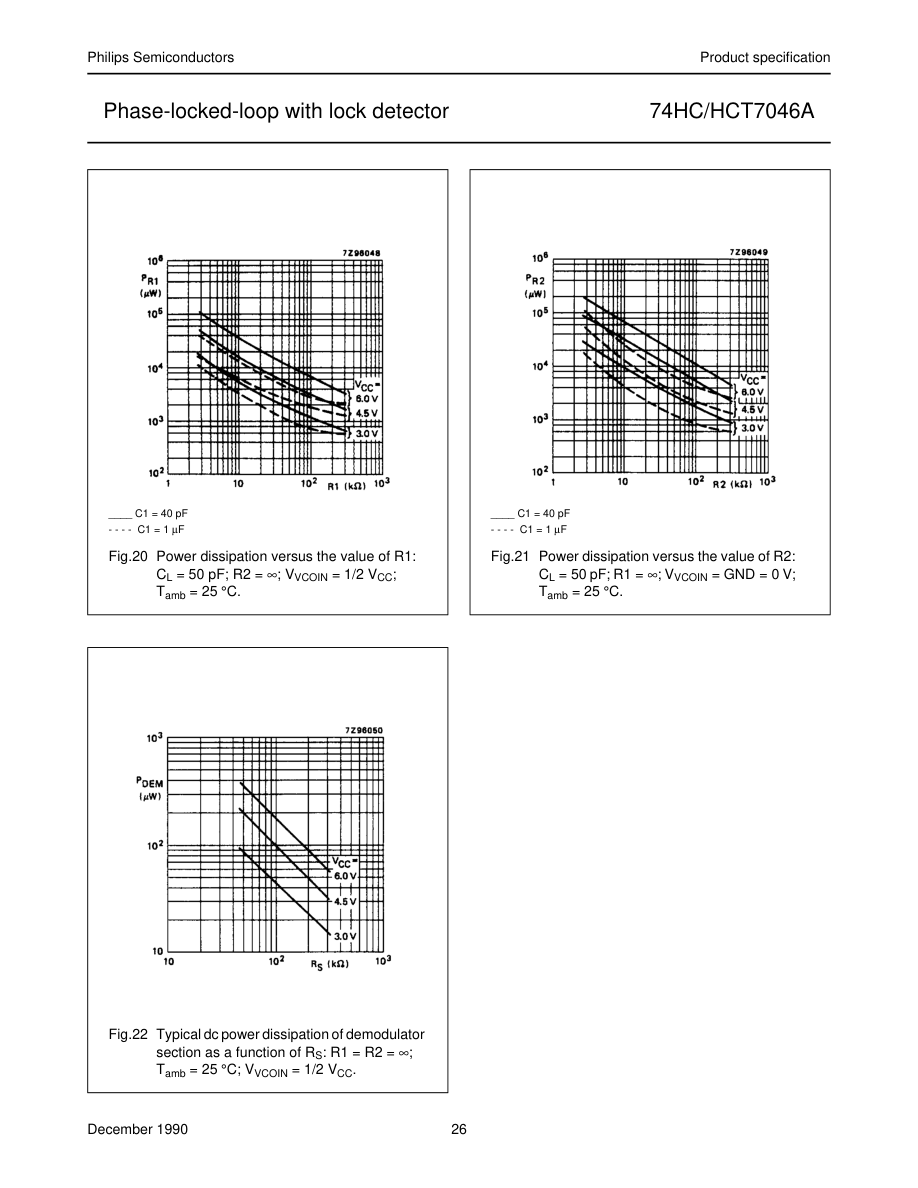
Page 27
APPLICATION INFORMATION
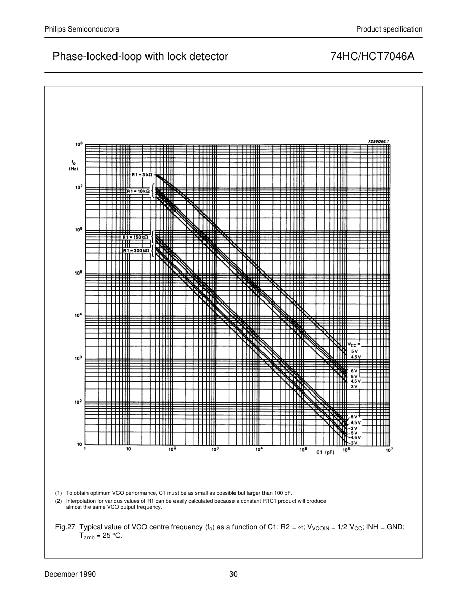
This information is a guide for the approximation of values of external components to be used with the 74HC/HCT7046 in a phase-lock-loop system. References should be made to Figs 27, 28 and 29 as indicated in the table.
Values of the selected components should be within the following ranges: R1 between 3 kΩ and 300 kΩ; R2 between 3 kΩ and 300 kΩ; R1 + R2 parallel value > 2.7 kΩ; C1 greater than 40 pF.
| SUBJECT | PHASE COMPARATOR | DESIGN CONSIDERATIONS |
| VCO frequency without extra offset | PC1, PC2 | VCO frequency characteristic With R2 = ∞ and R1 within the range 3 kΩ< R1 < 300 kΩ, the characteristics of the VCO operation will be as shown in Fig. 23. (Due to R1, C1 time constant a small offset remains when R2 = ∞.) Fig. 23 Frequency characteristic of VCO operating without offset: f = centre frequency; 2f = frequency lock range. o L |
| PC1 | Selection of R1 and C1 Given f , determine the values of R1 and C1 using Fig.27. o | |
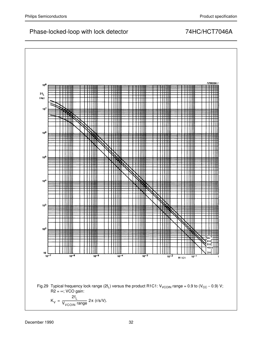
| PC2 | Given f and f , determine the values of R1 and C1 using Fig.27, max o use Fig.29 to obtain 2f and then use this to calculate f L min. |
Page 28
| SUBJECT | PHASE COMPARATOR | DESIGN CONSIDERATIONS |
| VCO frequency with extra offset | PC1, PC2 | VCO frequency characteristic With R1 and R2 within the ranges 3 kΩ< R1 < 300 kΩ, 3 kΩ< R2 < 300 kΩ, the characteristics of the VCO operation will be as shown in Fig. 24. Fig. 24 Frequency characteristic of VCO operating with offset: f = centre frequency; 2f = frequency lock range. o L |
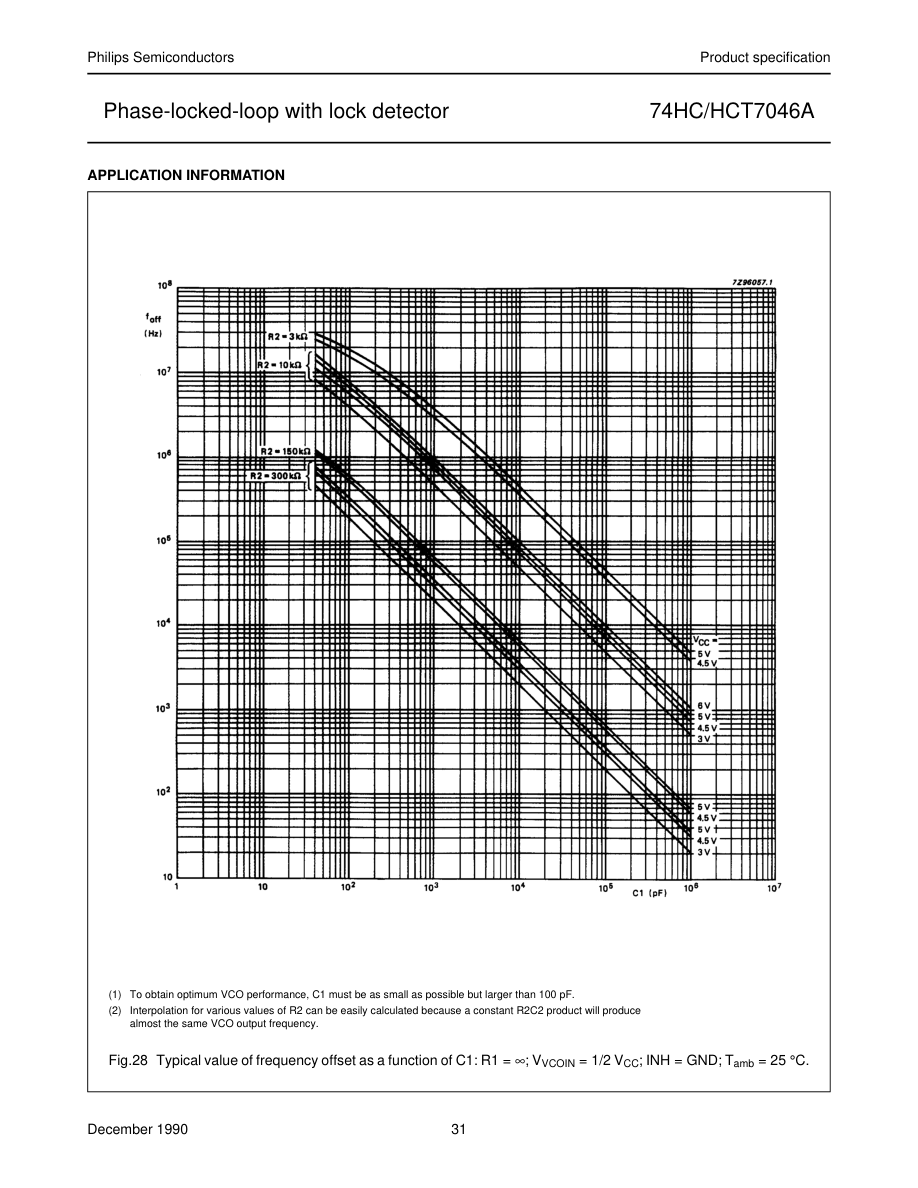
| PC1, PC2 | Selection of R1, R2 and C1 Given f and f , determine the value of product R1C1 by using Fig.29. 0 L Calculate f from the equation f = f −1.6f L. off off o Obtain the values of C1 and R2 by using Fig.28. Calculate the value of R1 from the value of C1 and the product R1C1. |
Page 29

| SUBJECT | PHASE COMPARATOR | DESIGN CONSIDERATIONS |
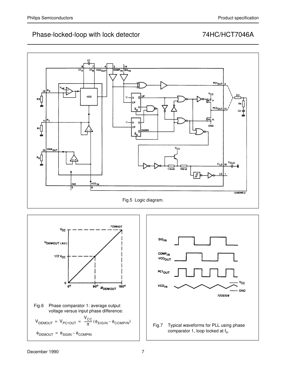
| PLL conditions with no signal at the SIG input IN | PC1 | VCO adjusts to f with φ = 90° and V = 1/2 V (see Fig.6). o DEMOUT VCOIN CC |
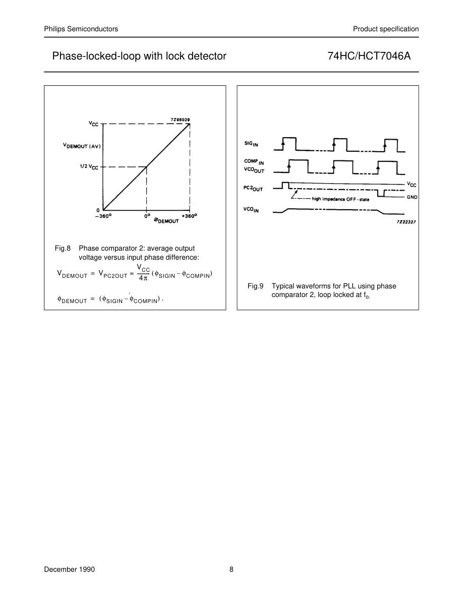
| PC2 | VCO adjusts to f with φ = −360° and V = min. (see Fig.8). o DEMOUT VCOIN | |
| PLL frequency capture range | PC1, PC2 | Loop filter component selection (a) τ = R3 x C2 (b) amplitude characteristic (c) pole-zero diagram Fig. 25 Simple loop filter for PLL without offset; R3 ≥500 Ω. |
| (a) τ1 = R3 x C2; (b) amplitude characteristic (c) pole-zero diagram τ2 = R4 x C2; τ3 = (R3 + R4) x C2 Fig. 26 Simple loop filter for PLL with offset; R3 + R4 ≥500 Ω. | ||
| PLL locks on harmonics at centre frequency | PC1 | yes |
| PC2 | no | |
| noise rejection at signal input | PC1 | high |
| PC2 | low | |
| AC ripple content when PLL is locked | PC1 | f = 2f i, large ripple content at φ = 90° r DEMOUT |
| PC2 | f = f i, small ripple content at φ = 0° r DEMOUT |
Page 30
Page 31
Page 32
Page 33
APPLICATION INFORMATION
Lock-detection circuit The built-in lock-detection circuit will only work when used in conjunction with the phase comparator PC2. The lock-indication is derived from the phase error between SIGIN and COMPIN. The PC2 has a typical phase error of zero degrees over the entire VCO operating range. However, to remain in-lock the circuit requires some small adjustments. The variation is dependent on the loop parameters and back-lash time (typically 5 ns). Depending
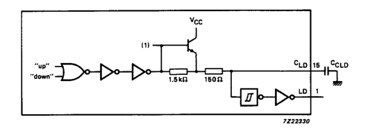
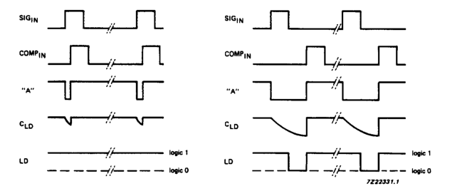
on the application, the phase error can be defined as the limit, a phase error of greater magnitude would be considered out-of-lock. An example of an in-lock detection circuit using the “7046A” is shown in Fig.30. If the PLL is in-lock, only very small pulses will come from the “up” or “down” connections of PC2. These pulses are filtered out by a RC network. A Schmitt trigger produces a steady state level, a HIGH level indicates an in-lock condition and a pulsed output indicates an out-of-lock condition as shown in Fig.31.
See Fig.31 for input waveform.
Fig.30 An example of an in-lock detection circuit using the “7046A”.
(a)
(b)
Fig.31 Waveforms showing the lock detection process; (a) in-lock; (b) out-of-lock.
Page 34
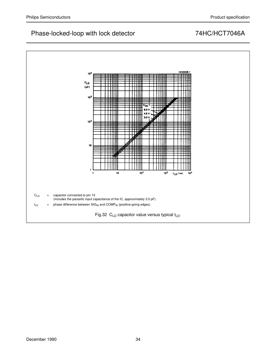
Page 35
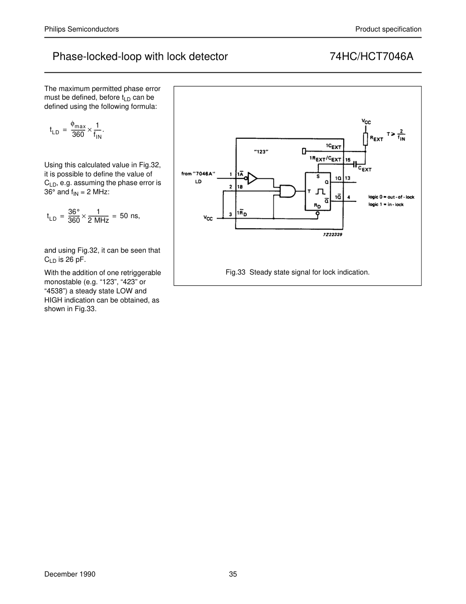
Page 36
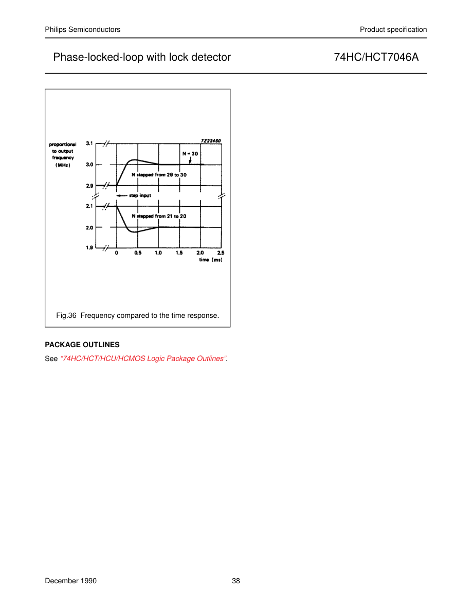
PLL design example The frequency synthesizer, used in the design example shown in Fig.34, has the following parameters: Output frequency: 2 MHz to 3 MHz frequency steps : 100 kHz settling time
: 1 ms
overshoot
: < 20%
The open-loop gain is H (s) x G (s) = Kp × Kf × Ko × Kn.
Where: Kp = phase comparator gain = low-pass filter transfer gain Kf Ko = Kv/s VCO gain Kn = 1/n divider ratio
The programmable counter ratio Kn can be found as follows: fout 2 MHz
Nmin. ----------- ---------------------- 20 = =
=
fstep 100 kHz
fout 3 MHz = ----------- = ---------------------- = 30 Nmax. fstep 100 kHz
The VCO is set by the values of R1, R2 and C1, R2 = 10 kΩ (adjustable). The values can be determined using the information in the section “DESIGN CONSIDERATIONS”. With fo = 2.5 MHz and fL = 500 kHz this gives the following values (VCC = 5.0 V): R1 = 10 kΩ R2 = 10 kΩ C1 = 500 pF The VCO gain is: 2fL × 2 × π
1 MHz
= ---------------------------------------------- = = ----------------- × 2π ≈ 2 × 10⁶ r/s/v KV
3.2
– 0.9) 0.9 – ( VCC
The gain of the phase comparator is: VCC ------------ 0.4 V/r. Kp = = 4 × π
The transfer gain of the filter is given by: 1 + τ2s Kf = ------------------------------------- 1 + ( + ) s τ1 τ2
Where: τ1 R3C2 and τ2
= R4C2.
=
The characteristics equation is: 1 + H (s) × G (s) = 0. This results in:
Kp Kv Kn
1 + × × × Kp Kv Kn τ2
× ×
s2 + ----------------------------------------------------- s --------------------------------
= 0.
+
( + )
( + )
τ1 τ2
τ1 τ2
The natural frequency ωn is defined as follows:
˙ Kp Kv Kn × × = --------------------------------. ωn ( + ) τ1 τ2
and the damping value ζ is defined as follows:
1 + × × × Kp Kv Kn τ2 1
.
---------- ----------------------------------------------------- ζ = × 2ωn
+ τ1 τ2
The overshoot and settling time percentages are now used to determine ωn. From Fig.35 it can be seen that the damping ratio ζ = 0.8 will produce an overshoot of less than 20% and settle to within 5% at ωnt = 4.5. The required settling time is 1 ms. This results in: 5 5 = 5 × 10³ r/s.
= = t--- 0.001 --------------- ωn
Rewriting the equation for natural frequency results in:
Kp Kv Kn × ×
( + ) = --------------------------------. τ1 τ2
2 ωn
The maximum overshoot occurs at Nmax.:
0.4 × 2 × 106
= 0.0011 s.
( + ) =
--------------------------------- τ1 τ2
2 5000 × 30
When C2 = 470 nF, then
) × 2 × × ζ 1 +
–
( τ1 τ2
ωn
R4 ----------------------------------------------------------------- 790 Ω. =
=
Kp Kv Kn × ×
R3 is calculated using the damping ratio equation: τ1 R3 = – R4 = 2 kΩ. -------- C2
Page 37
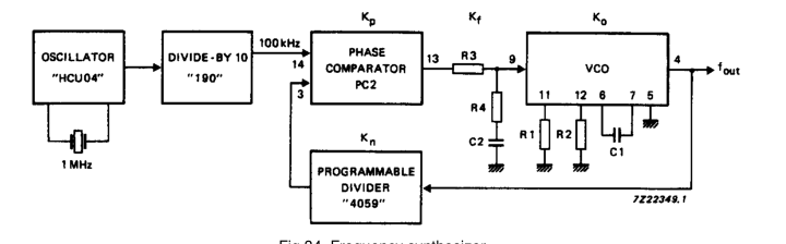
Fig.34 Frequency synthesizer.
Note For an extensive description and application example please refer to application note ordering number 9398 649 90011. Also available a computer design program for PLL’s ordering number 9398 961 10061.
MGA959
1.6
−0.6
= 0.3 ζ
1.4
−0.4
0.5
∆ω (t)
∆Φ (t)
e
e
0.707
∆ωe /ω n
∆Φe /ω n
1.0
1.2
−0.2
= 5.0 ζ
0
1.0
= 2.0 ζ
0.8
0.2
0.6
0.4
0.4
0.6
0.2
0.8
0
1.0
0 1 2 3 4 5 6 7 8 ω nt
Fig.35 Type 1, second order frequency step response.
Since the output frequency is proportional to the VCO control voltage, the PLL frequency response can be observed with an oscilloscope by monitoring pin 9 of the VCO. The average frequency response, as calculated by the Laplace method, is found experimentally by smoothing this voltage at pin 9 with a simple RC filter, whose time constant is long compared to the phase detector sampling rate but short compared to the PLL response time.
Page 38