Download PDF
74HC7030 PHILIPS
Document overview
- PDF pages: 22
Technical content
Page 1
Page 2
FEATURES
- Synchronous or asynchronous operation
- 3-state outputs
- Master-reset input to clear control functions
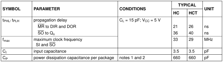
- 33 MHz (typ.) shift-in, shift-out rates with or without flags
- Very low power consumption
- Cascadable to 25 MHz (typ.)
- Readily expandable in word and bit dimensions
- Pinning arranged for easy board layout: input pins directly opposite output pins
- Output capability: standard
- ICC category: LSI
GENERAL DESCRIPTION
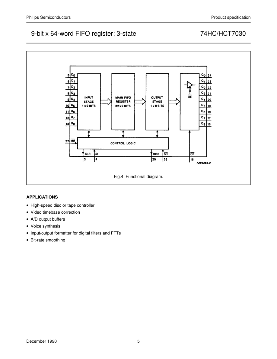
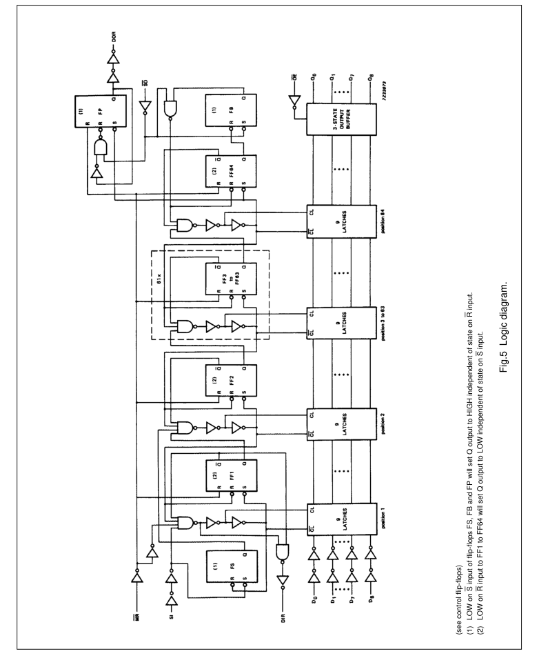
The 74HC/HCT7030 are high-speed Si-gate CMOS devices specified in compliance with JEDEC standard no. 7A. The 74HC/HCT7030 is an expandable, First-In First-Out (FIFO) memory organized as 64 words by 9 bits. A 33 MHz data-rate makes it ideal for high-speed applications. Even at high frequencies, the ICC dynamic is very low (fmax = 18 MHz; VCC = 5 V produces a dynamic ICC of 80 mA). If the device is not continuously operating at fmax, then ICC will decrease proportionally. With separate controls for shift-in (SI) and shift-out (SO), reading and writing operations are completely independent, allowing synchronous and asynchronous data transfers. Additional controls include a master-reset
input (MR) and an output enable input (OE). Flags for data-in-ready (DIR) and data-out-ready (DOR) indicate the status of the device. Devices can be interconnected easily to expand word and bit dimensions. All output pins are directly opposite the corresponding input pins thus simplifying board layout in expanded applications.
INPUTS AND OUTPUTS
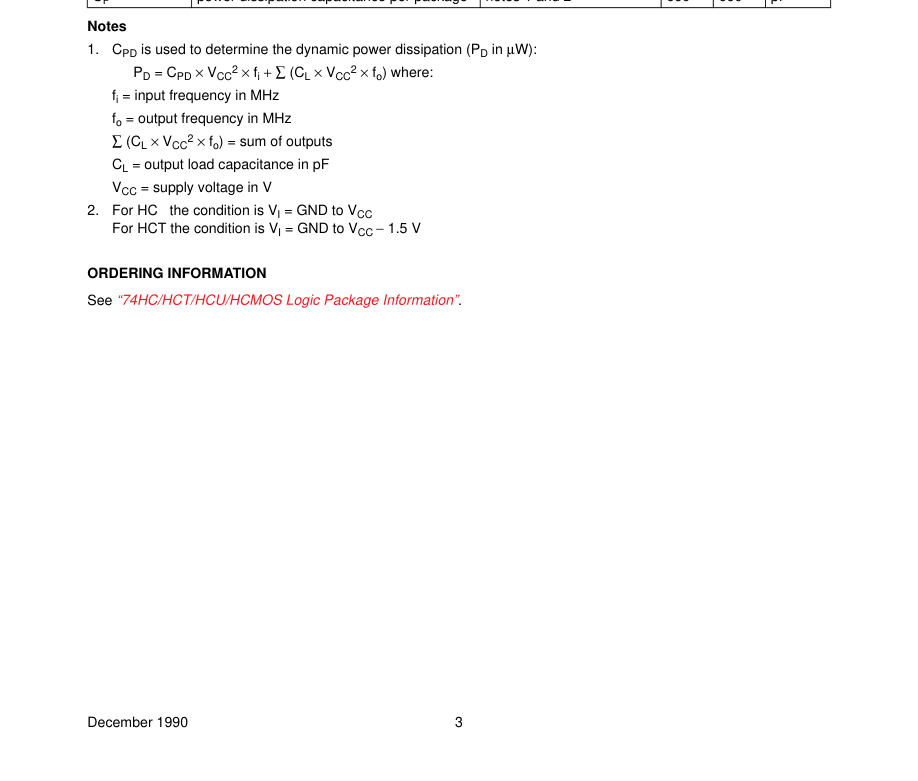
Data inputs (D0 to D8) As there is no weighting of the inputs, any input can be assigned as the MSB. The size of the FIFO memory can be reduced from the 9 × 64 configuration, i.e. 8 × 64, 7 × 64, down to 1 × 64, by tying unused data input pins to VCC or GND.
Data outputs (Q0 to Q8) As there is no weighting of the outputs, any output can be assigned as the MSB. The size of the FIFO memory can be reduced from the 9 × 64 configuration as described for data inputs. In a reduced format, the unused data output pins must be left open circuit.
Master-reset (MR) When MR is LOW, the control functions within the FIFO are cleared, and data content is declared invalid. The data-in-ready (DIR) flag is set HIGH and the data-out-ready (DOR) flag is set LOW. The output stage remains in the state of the last word that was shifted out, or in the random state existing at power-up.
Status flag outputs (DIR, DOR) Indication of the status of the FIFO is given by two status flags, data-in-ready (DIR) and data-out-ready (DOR):
DIR = HIGH indicates the input stage is empty and ready to accept valid data DIR = LOW indicates that the FIFO is full or that a previous shift-in operation is not complete (busy) DOR = HIGH assures valid data is present at the outputs Q0 to Q8 (does not indicate that new data is awaiting transfer into the output stage) DOR = LOW indicates the output stage is busy or there is no valid data
Shift-in control (SI) Data is loaded into the input stage on a LOW-to-HIGH transition of SI. A HIGH-to-LOW transition triggers an automatic data transfer process (ripple through). If SI is held HIGH during reset, data will be loaded at the rising edge of the MR signal.
Shift-out control (SO) A LOW-to-HIGH transition of SO causes the DOR flags to go LOW. A HIGH-to-LOW transition of SO causes upstream data to move into the output stage, and empty locations to move towards the input stage (bubble-up).
Output enable (OE) The outputs Q0 to Q8 are enabled when OE = LOW. When OE = HIGH the outputs are in the high impedance OFF-state.
Page 3
Page 4
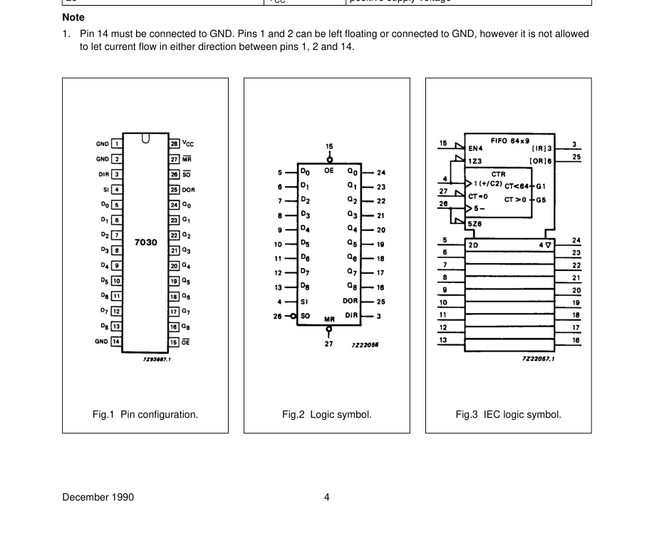
| PIN NO. | SYMBOL | NAME AND FUNCTION |
|---|---|---|
| 1, 2, 14 3 4 5, 6, 7, 8, 9, 10, 11, 12, 13 15 24, 23, 22, 21, 20, 19, 18, 17, 16 25 26 27 28 | GND DIR SI D to D 0 8 OE Q to Q 0 8 DOR SO MR V CC | ground (0 V) data-in-ready output shift-in input (LOW-to-HIGH, edge-triggered) parallel data inputs output enable input (active LOW) 3-state parallel data outputs data-out-ready output shift-out input (HIGH-to-LOW, edge-triggered) asynchronous master-reset input (active LOW) positive supply voltage |
Page 5
Page 6
FUNCTIONAL DESCRIPTION
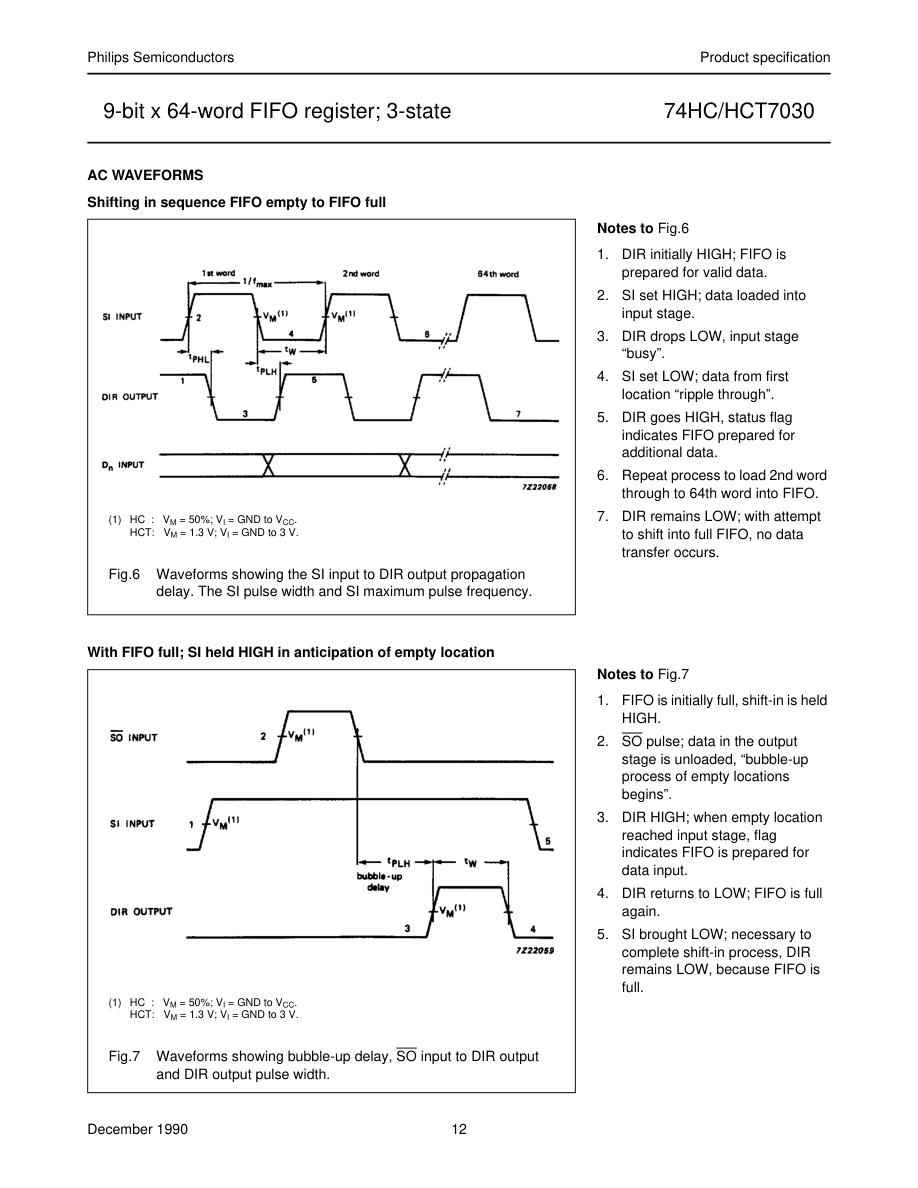
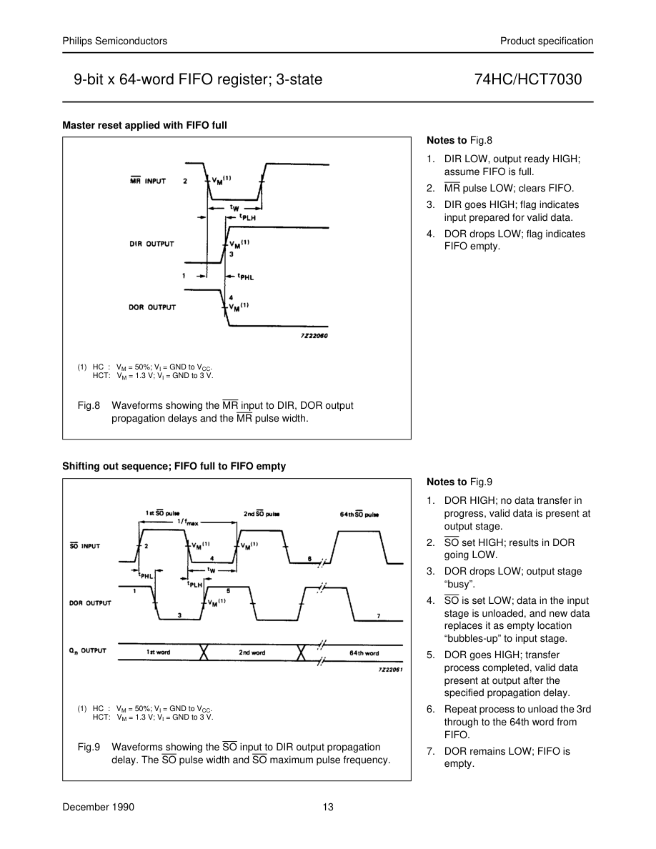
Data input Following power-up, the master-reset (MR) input is pulsed LOW to clear the FIFO memory (see Fig.8). The data-in-ready flag (DIR = HIGH) indicates that the FIFO input stage is empty and ready to receive data. When DIR is valid (HIGH), data present at D0 to D8 can be shifted-in using the SI control input. With SI = HIGH, data is shifted into the input stage and a busy indication is given by DIR going LOW. The data remains at the first location in the FIFO until SI is set to LOW. With SI = LOW data moves through the FIFO to the output stage, or to the last empty location. If the FIFO is not full after the SI pulse, DIR again becomes valid (HIGH) to indicate that space is available in the FIFO. The
DIR flag remains LOW if the FIFO is full (see Fig.6). The SI pulse must be made LOW in order to complete the shift-in process. With the FIFO full, SI can be held HIGH until a shift-out (SO) pulse occurs. Then, following a shift-out of data, an empty location appears at the FIFO input and DIR goes HIGH to allow the next data to be shifted-in. This remains at the first FIFO location until SI again goes LOW (see Fig.7).
Data transfer After data has been transferred from the input stage of the FIFO following SI = LOW, data moves through the FIFO asynchronously and is stacked at the output end of the register. Empty locations appear at the input end of the FIFO as data moves through the device.
Data output The data-out-ready flag (DOR = HIGH) indicates that there is valid data at the output (Q0 to Q8). The initial master-reset at power-on (MR = LOW) sets DOR to LOW (see Fig.8). After MR = HIGH, data shifted into the FIFO moves through to the output stage causing DOR to go HIGH. As the DOR flag goes HIGH, data can be shifted-out using the SO control input. With SO = HIGH, data in the output stage is shifted out and a busy indication is given by DOR going LOW. When SO is made LOW, data moves through the FIFO to fill the output stage and an empty location appears at the input stage. When the output stage is filled DOR goes HIGH, but if the last of the
valid data has been shifted out leaving the FIFO empty the DOR flag remains LOW (see Fig.9). With the FIFO empty, the last word that was shifted-out is latched at the output Q0 to Q8.
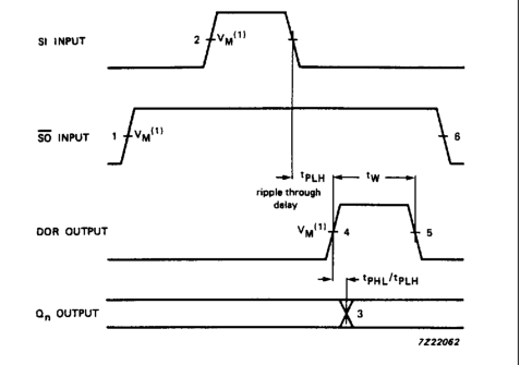
With the FIFO empty, the SO input can be held HIGH until the SI control input is used. Following an SI pulse, data moves through the FIFO to the output stage, resulting in the DOR flag pulsing HIGH and a shift-out of data occurring. The SO control must be made LOW before additional data can be shifted out (see Fig.10).
High-speed burst mode If it is assumed that the shift-in/shift-out pulses are not applied until the respective status flags are valid, it follows that the shift-in/shift-out rates are determined by the status flags. However, without the status flags a high-speed burst mode can be implemented. In this mode, the burst-in/burst-out rates are determined by the pulse widths of the shift-in/shift-out inputs and burst rates of 35 MHz can be obtained. Shift pulses can be applied without regard to the status flags but shift-in pulses that would overflow the storage capacity of the FIFO are not allowed (see Figs 11 and 12).
Expanded format With the addition of a logic gate, the FIFO is easily expanded to increase word length (see Fig.17). The basic operation and timing are identical to a single FIFO, with the exception of an additional gate delay on the flag outputs. If during application, the following occurs:
- SI is held HIGH when the FIFO is empty, some additional logic is required to produce a composite DIR pulse (see Figs 7 and 18).
- SO is held HIGH when the FIFO is full, some additional logic is required to produce a composite DOR pulse (see Figs 10 and 18).
Due to the part-to-part spread of the ripple through time, the flag signals of FIFOA and FIFOB will not always coincide and the AND-gate will not produce a composite flag signal. The solution is given in Fig.18. The “7030” is easily cascaded to increase the word capacity and no external components are needed. In the cascaded configuration, all necessary communications and timing are performed by the FIFOs. The intercommunication speed is determined by the minimum flag pulse widths and the flag delays. The data rate of cascaded devices is typically 25 MHz. Word-capacity can be expanded to and beyond 128-words × 9-bits (see Fig.19).
Page 7

Page 8

Page 9

Page 10

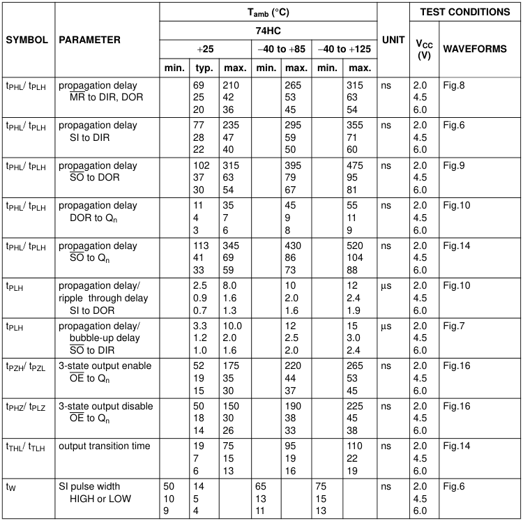
| SYMBOL | PARAMETER | T (°C) amb | UNIT | TEST CONDITIONS | |||||||
|---|---|---|---|---|---|---|---|---|---|---|---|
| 74HCT | V CC (V) | WAVEFORMS | |||||||||
| +25 | −40 to +85 | −40 to +125 | |||||||||
| min. | typ. | max. | min. | max. | min. | max. | |||||
| t / t PHL PLH | propagation delay MR to DIR, DOR | 30 | 51 | 53 | 63 | ns | 4.5 | Fig.8 | |||
| t / t PHL PLH | propagation delay SI to DIR | 29 | 49 | 61 | 74 | ns | 4.5 | Fig.6 | |||
| t / t PHL PLH | propagation delay SO to DOR | 39 | 67 | 84 | 101 | ns | 4.5 | Fig.9 | |||
| t / t PHL PLH | propagation delay SO to Q n | 46 | 78 | 98 | 117 | ns | 4.5 | Fig.14 | |||
| t / t PHL PLH | propagation delay DOR to Q n | 7 | 12 | 15 | 18 | ns | 4.5 | Fig.10 | |||
| t PLH | propagation delay/ripple through delay SI to DOR | 0.9 | 1.6 | 2.0 | 2.4 | µs | 4.5 | Fig.10 | |||
| t PLH | propagation delay/ bubble-up delay SO to DIR | 1.2 | 2.0 | 2.5 | 3.0 | µs | 4.5 | Fig.7 | |||
| t / t PZH PZL | 3-state output enable OE to Q n | 20 | 35 | 44 | 53 | ns | 4.5 | Fig.16 | |||
| t / t PHZ PLZ | 3-state output disable OE to Q n | 19 | 35 | 44 | 53 | ns | 4.5 | Fig.16 | |||
| t / t THL TLH | output transition time | 7 | 15 | 19 | 22 | ns | 4.5 | Fig.14 | |||

Page 11

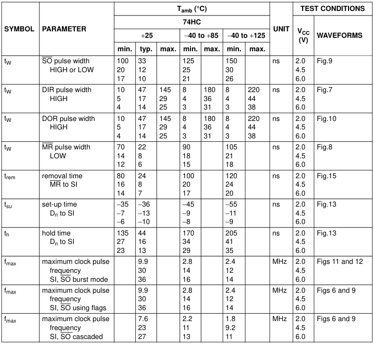
| SYMBOL | PARAMETER | T (°C) amb | UNIT | TEST CONDITIONS | |||||||
|---|---|---|---|---|---|---|---|---|---|---|---|
| 74HCT | V CC (V) | WAVEFORMS | |||||||||
| +25 | −40 to +85 | −40 to +125 | |||||||||
| min. | typ. | max. | min. | max. | min. | max. | |||||
| t W | SI pulse width HIGH or LOW | 12 | 6 | 15 | 18 | ns | 4.5 | Fig.6 | |||
| t W | SO pulse width HIGH or LOW | 15 | 9 | 19 | 22 | ns | 4.5 | Fig.9 | |||
| t W | DIR pulse width HIGH | 7 | 22 | 37 | 6 | 46 | 6 | 56 | ns | 4.5 | Fig.7 |
| t W | DOR pulse width HIGH | 6 | 20 | 35 | 5 | 44 | 5 | 53 | ns | 4.5 | Fig.10 |
| t W | MR pulse width LOW | 18 | 10 | 23 | 27 | ns | 4.5 | Fig.8 | |||
| t rem | removal time MR to SI | 18 | 10 | 23 | 27 | ns | 4.5 | Fig.15 | |||
| t su | set-up time D to SI n | −5 | −16 | −4 | −4 | ns | 4.5 | Fig.13 | |||
| t h | hold time D to SI n | 30 | 18 | 38 | 45 | ns | 4.5 | Fig.13 | |||
| f max | maximum clock pulse frequency SI, SO burst mode | 15 | 26 | 12 | 10 | MHz | 4.5 | Figs 11 and 12 | |||
| f max | maximum clock pulse frequency SI, SO using flags | 15 | 26 | 12 | 10 | MHz | 4.5 | Figs 6 and 9 | |||
| f max | maximum clock pulse frequency SI, SO cascaded | 13 | 22 | 10 | 8.6 | MHz | 4.5 | Figs 6 and 9 | |||
Page 12
Page 13
Page 14
With FIFO empty; SO is held HIGH in anticipation
(1) HC : VM = 50%; VI = GND to VCC. HCT: VM = 1.3 V; VI = GND to 3 V.
Fig.10 Waveforms showing ripple through delay SI input to DOR output, DOR output pulse width and propagation delay from the DOR pulse to the Qn output.
Shift-in operation; high-speed burst mode
Notes to Fig.10 1. FIFO is initially empty, SO is held HIGH. 2. SI pulse; loads data into FIFO and initiates ripple through process. 3. DOR flag signals the arrival of valid data at the output stage. 4. Output transition; data arrives at output stage after the specified propagation delay between the rising edge of the DOR pulse to the Qn output. 5. DOR goes LOW; FIFO is empty again. 6. SO set LOW; necessary to complete shift-out process. DOR remains LOW, because FIFO is empty.
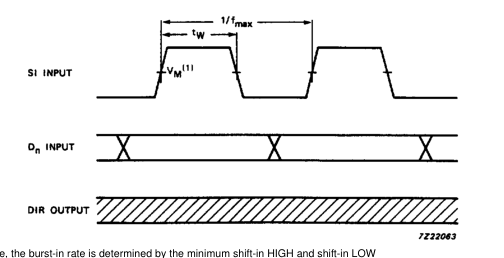
In the high-speed mode, the burst-in rate is determined by the minimum shift-in HIGH and shift-in LOW specifications. The DIR status flag is a don’t care condition, and a shift-in pulse can be applied regardless of the flag. A SI pulse which would overflow the storage capacity of the FIFO is ignored. (1) HC : VM = 50%; VI = GND to VCC. HCT: VM = 1.3 V; VI = GND to 3 V.
Fig.11 Waveforms showing SI minimum pulse width and SI maximum pulse frequency, in high-speed shift-in burst mode.
Page 15
Shift-out operation; high-speed burst mode
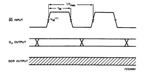
In the high-speed mode, the burst-out rate is determined by the minimum shift-out HIGH and shift-out LOW specifications. The DOR flag is a don’t care condition and a SO pulse can be applied without regard to the flag. (1) HC : VM = 50%; VI = GND to VCC. HCT: VM = 1.3 V; VI = GND to 3 V.
Fig.12 Waveforms showing SO minimum pulse width and maximum pulse frequency, in high-speed shift-out
burst mode.
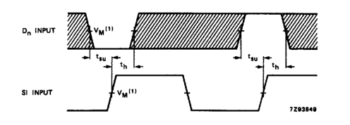
The shaded areas indicate when the input is permitted to change for predictable output performance. (1) HC : VM = 50%; VI = GND to VCC. HCT: VM = 1.3 V; VI = GND to 3 V.
Fig.13 Waveforms showing hold and set-up times for Dn input to SI input.
Page 16
Page 17
APPLICATION INFORMATION
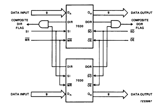
The PC74HC/HCT7030 is easily expanded to increase word length. Composite DIR and DOR flags are formed with the addition of an AND gate. The basic operation and timing are identical to a single FIFO, with the exception of an added gate delay on the flags.
Fig.17 Expanded FIFO for increased word length; 64 words × 18 bits.
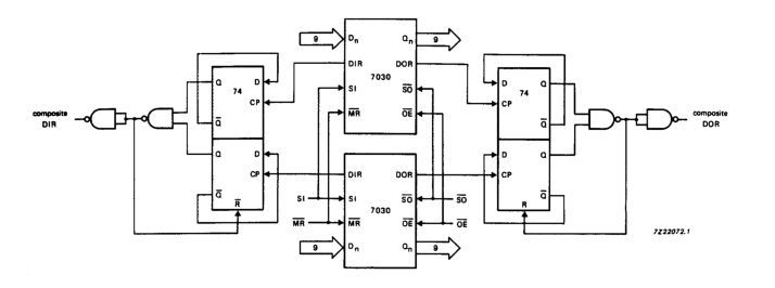
This circuit is only required if the SI input is constantly held HIGH, when the FIFO is empty and the automatic shift-in cycles are started or if SO output is constantly held HIGH, when the FIFO is full and the automatic shift-out cycles are started (see Figs 7 and 10).
Fig.18 Expanded FIFO for increased word length.
Page 18
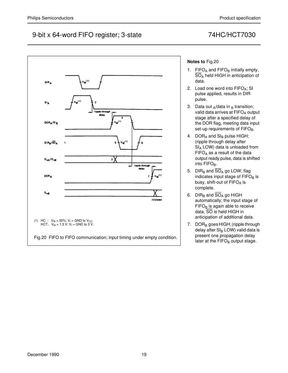
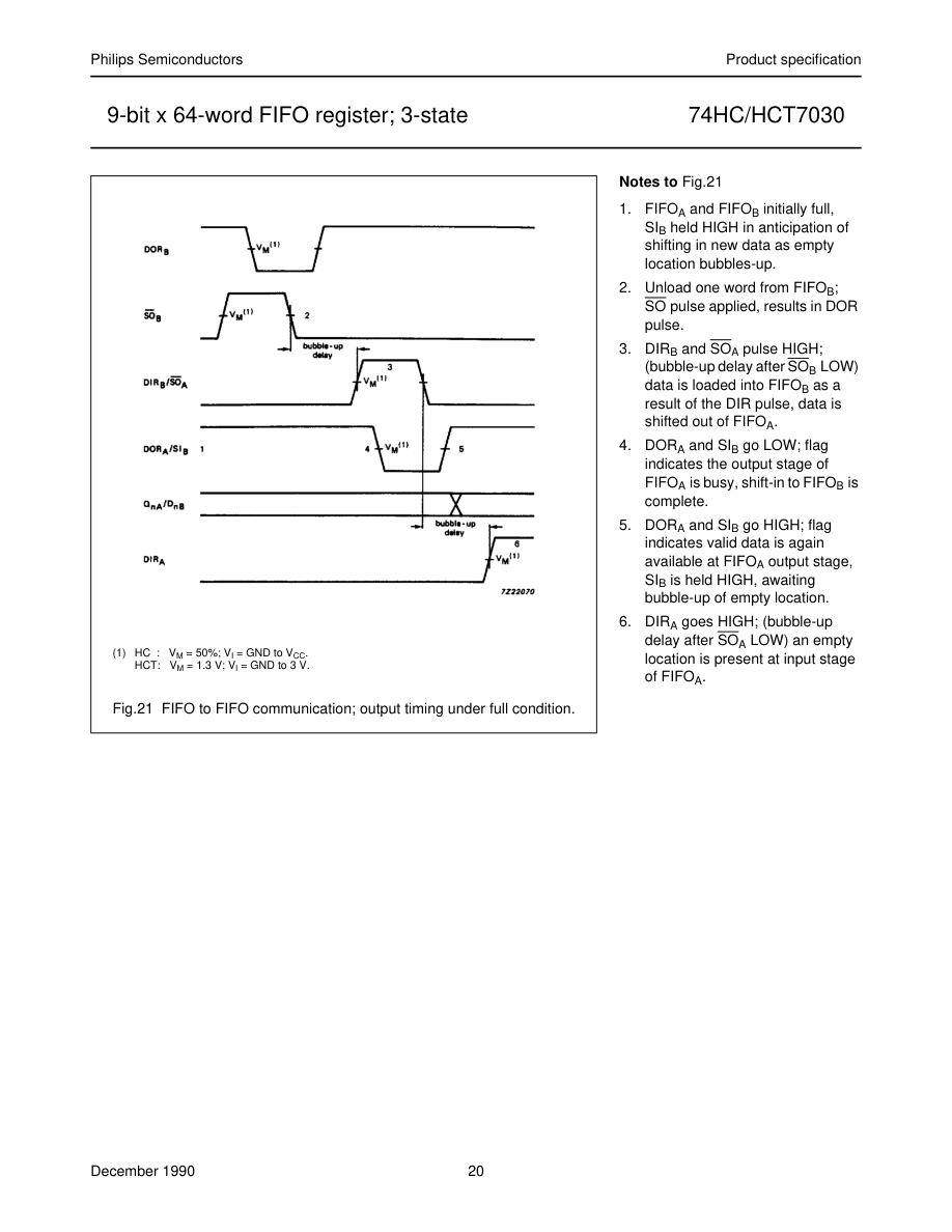
Expanded format Fig.19 shows two cascaded FIFOs providing a capacity of 128 words × 9 bits. Fig.20 shows the signals on the nodes of both FIFOs after the application of a SI pulse, when both FIFOs are initially empty. After a rippled through delay, data arrives at the output of FIFOA. Due to SOA being HIGH, a DOR pulse is generated. The requirements of SIB and DnB are satisfied by the DORA pulse width and the timing between the rising edge of DORA and QnA. After a second ripple through delay, data arrives at the output of FIFOB. Fig.21 shows the signals on the nodes of both FIFOs after the application of a SOB pulse, when both FIFOs are initially full. After a bubble-up delay a DIRB pulse is generated, which acts as a SOA pulse for FIFOA. One word is transferred
from the output of FIFOA to the input of FIFOB. The requirements of the SOA pulse for FIFOA is satisfied by the pulse width of DORB. After a second bubble-up delay an empty space arrives at DnA, at which time DIRA goes HIGH. Fig.22 shows the waveforms at all external nodes of both FIFOs during a complete shift-in and shift-out sequence.
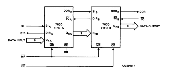
The PC74HC/HCT7030 is easily cascaded to increase word capacity without any external circuitry. In cascaded format, all necessary communications are handled by the FIFOs. Figs 17 to 19 demonstrate the intercommunication timing between FIFOA and FIFOB. Fig.22 gives an overview of pulses and timing of two cascaded FIFOs, when shifted full and shifted empty again.
Fig.19 Cascading for increased word capacity; 128 words × 9 bits.
Page 19
Page 20
Page 21
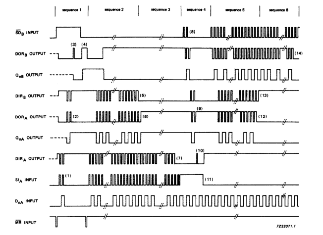
Sequence 1 (Both FIFOs empty, starting shift-in process): After a MR pulse has been applied FIFOA and FIFOB are empty. The DOR flags of FIFOA and FIFOB go LOW due to no valid data being present at the outputs. The DIR flags are set HIGH due to the FIFOs being ready to accept data. SOB is held HIGH and two SIA pulses are applied (1). These pulses allow two data words to ripple through to the output stage of FIFOA and to the input stage of FIFOB (2). When data arrives at the output of FIFOB, a DORB pulse is generated (3). When SOB goes LOW, the first bit is shifted out and a second bit ripples through to the output after which DORB goes HIGH (4). Sequence 2 (FIFOB runs full):
After the MR pulse, a series of 64 SI pulses are applied. When 64 words are shifted in, DIRB remains LOW due to FIFOB being full (5). DORA goes LOW due to FIFOA being empty. Sequence 3 (FIFOA runs full): When 65 words are shifted in, DORA remains HIGH due to valid data remaining at the output of FIFOA. QnA remains HIGH, being the polarity of the 65th data word (6). After the 128th SI pulse, DIR remains LOW and both FIFOs are full (7). Additional pulses have no effect. Sequence 4 (Both FIFOs full, starting shift-out process): SIA is held HIGH and two SOB pulses are applied (8). These pulses shift out two words and thus allow two empty locations to bubble-up to the input stage of FIFOB, and proceed to FIFOA (9). When the first empty
location arrives at the input of FIFOA, a DIRA pulse is generated (10) and a new word is shifted into FIFOA. SIA is made LOW and now the second empty location reaches the input stage of FIFOA, after which DIRA remains HIGH (11). Sequence 5 (FIFOA runs empty): At the start of sequence 5 FIFOA contains 63 valid words due to two words being shifted out and one word being shifted in in sequence 4. An additional series of SOB pulses are applied. After 63 SOB pulses, all words from FIFOA are shifted into FIFOB. DORA remains LOW (12). Sequence 6 (FIFOB runs empty): After the next SOB pulse, DIRB remains HIGH due to the input stage of FIFOB being empty (13). After
another 63 SOB pulses, DORB remains LOW due to both FIFOs being empty (14). Additional SOB pulses have no effect. The last word remains available at the output Qn.
Fig.22 Waveforms showing the functionality and intercommunication between two FIFOs (refer to Fig.19).
Page 22