Download PDF
74HC652 PHILIPS
Document overview
- PDF pages: 10
Technical content
Page 1
Page 2
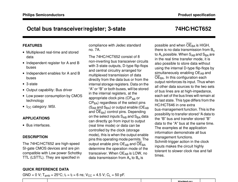
| SYMBOL | PARAMETER | CONDITIONS | TYPICAL | UNIT | |
|---|---|---|---|---|---|
| HC | HCT | ||||
| t /t PLH PZL | propagation delay A n/B to B /A n n n | C = 15 pF; L V = 5 V CC | 13 | 13 | ns |
| propagation delay CP AB/CP to B /A BA n n | 18 | 20 | ns | ||
| propagation delay S AB/S to B /A BA n n | 20 | 23 | ns | ||
| t /t PHZ PZL | 3-state output enable time OE AB/OE to B n/A BA n | 14 | 15 | ns | |
| t /t PHZ PLZ | 3-state output disable time OE AB/OE to B n/A BA n | 12 | 13 | ns | |
| f max | maximum clock frequency | 92 | 92 | MHz | |
| C I | input capacitance | 3.5 | 3.5 | pF | |
| C PD | power dissipation capacitance per channel | notes 1 and 2 | 26 | 28 | pF |
Page 3
| TYPE NUMBER | PACKAGE | |||
|---|---|---|---|---|
| PINS | PIN POSITION | MATERIAL | CODE | |
| 74HC/HCT652N | 24 | DIL | plastic | SOT101L |
| 74HC/HCT652D | 24 | SO | plastic | SOT137A |
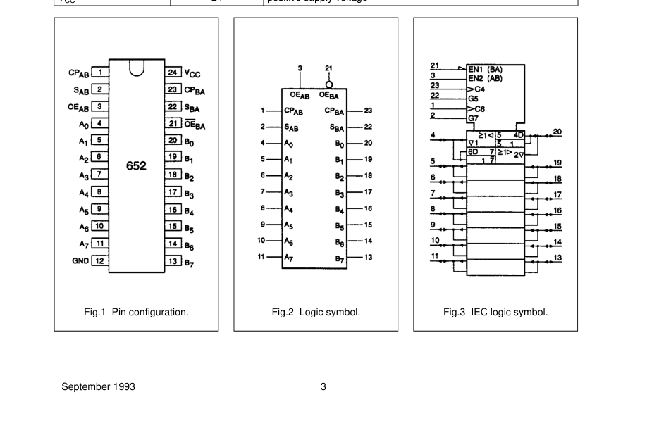
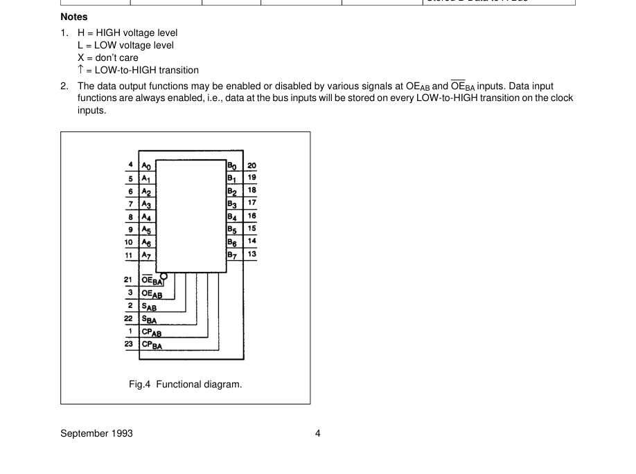
PINNING
| SYMBOL | PIN | DESCRIPTION |
|---|---|---|
| CP AB | 1 | A to B clock input |
| S AB | 2 | select A to B source input |
| OE AB | 3 | output enable A to B input |
| A ..A 0 7 | 4..11 | A data inputs/outputs |
| GND | 12 | ground (0 V) |
| B ..B 7 0 | 13..20 | B data inputs/outputs |
| OE BA | 21 | output enable B to A input |
| S BA | 22 | select B to A source input |
| CP BA | 23 | B to A clock input |
| V CC | 24 | positive supply voltage |
Page 4
| INPUTS (1) | DATA I/O (2) | OPERATION OR FUNCTION | |||
| OE OE AB BA | CP CP AB BA | S S AB BA | A THRU A 1 8 | B THRU B 1 8 | HC/HCT652 |
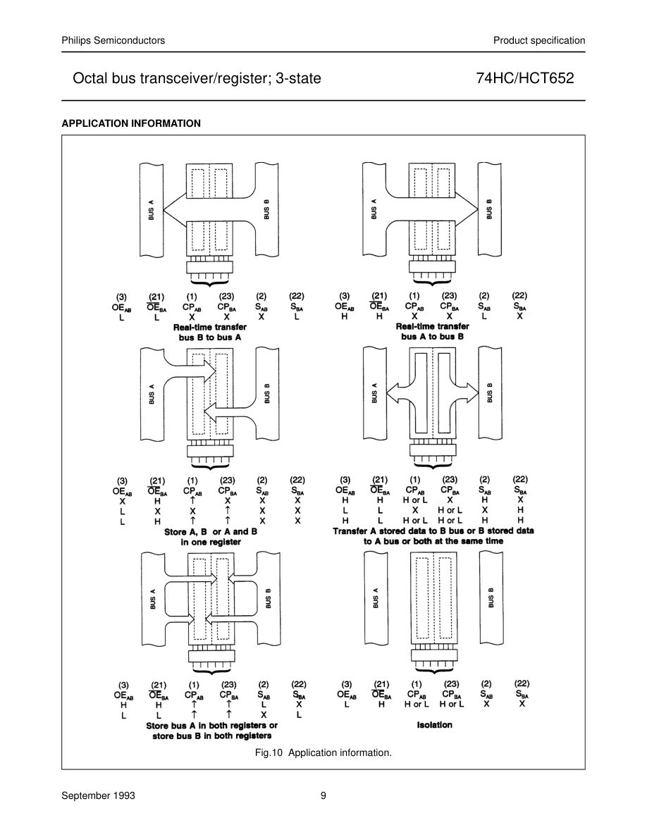
| L H L H | H or L H or L ↑ ↑ | X X X X | Input | Input | Isolation Store A and B data |
| X H H H | ↑ H or L ↑ ↑ | X X L X | Input Input | Not specified Output | Store A, Hold B Store A in both registers |
| L X L L | H or L ↑ ↑ ↑ | X X X L | Not specified Ouput | Input Input | Hold A, Store B Store B in both registers |
| L L L L | X X X H or L | X L X H | Ouput | Input | Real Time B Data to A Bus Stored B Data to A Bus |
| H H H H | X X H or L X | L X H X | Input | Output | Real Time A Data to B Bus Stored A Data to B Bus |
| H L | H or L H or L | H H | Output | Output | Stored A Data to B Bus and Stored B Data to A Bus |
Page 5
Page 6
Page 7
| INPUT | UNIT LOAD COEFFICIENT |
|---|---|
| S , S AB BA | 0.75 |
| A to A and B to B 0 7 0 7 | 0.75 |
| CP , CP AB BA | 1.50 |
| OE AB | 1.50 |
| OE BA | 1.50 |

| INPUT | PARAMETER | T (°C) amb | UNIT | TEST CONDITIONS | |||||||
|---|---|---|---|---|---|---|---|---|---|---|---|
| +25 | −40 to +85 | −40 to +125 | V CC (V) | WAVEFORMS | |||||||
| MIN. | TYP. | MAX. | MIN. | MAX. | MIN. | MAX. | |||||
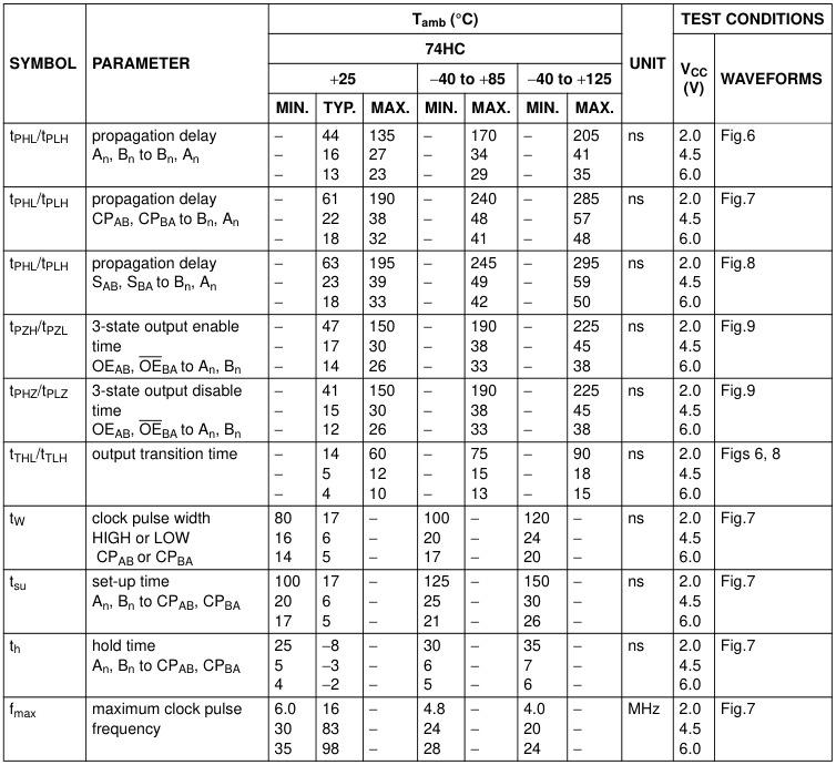
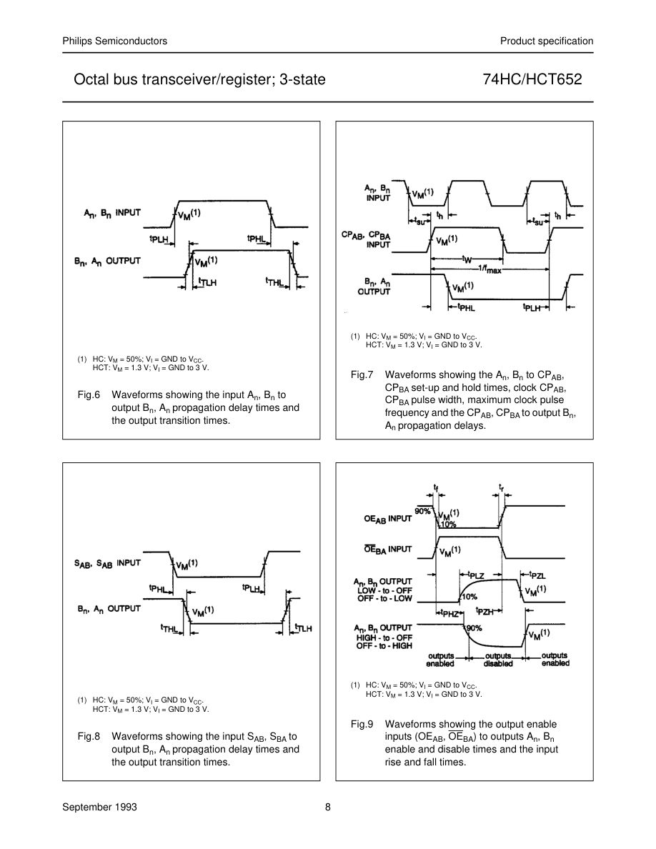
| t /t PHL PLH | propagation delay A , B to B , A n n n n | − | 16 | 27 | − | 34 | − | 41 | ns | 4.5 | Fig.6 |
| t /t PHL PLH | propagation delay CP AB, CP to B n, A BA n | − | 23 | 39 | − | 49 | − | 59 | ns | 4.5 | Fig.7 |
| t /t PHL PLH | propagation delay S AB, S to B n, A BA n | − | 27 | 46 | − | 55 | − | 66 | ns | 4.5 | Fig.8 |
| t /t PZH PZL | 3-state output enable time OE AB, OE to A n, B BA n | − | 18 | 33 | − | 41 | − | 50 | ns | 4.5 | Fig.9 |
| t /t PHZ PLZ | 3-state output disable time OE AB, OE to A n, B BA n | − | 16 | 35 | − | 44 | − | 53 | ns | 4.5 | Fig.9 |
| t /t THL TLH | output transition time | − | 5 | 12 | − | 15 | − | 18 | ns | 4.5 | Fig.6, 8 |
| t W | clock pulse width HIGH or LOW CP or CP AB BA | 16 | 6 | − | 20 | − | 24 | − | ns | 4.5 | Fig.7 |
| t su | set-up time A , B to CP , CP n n AB BA | 10 | 5 | − | 13 | − | 15 | − | ns | 4.5 | Fig.7 |
| t h | hold time A , B to CP , CP n n AB BA | 5 | −2 | − | 6 | − | 8 | − | ns | 4.5 | Fig.7 |
| f max | maximum clock pulse frequency | 30 | 83 | − | 24 | − | 20 | − | MHz | 4.5 | Fig.7 |

Page 8
Page 9
Page 10