Download PDF
74HC4514 PHILIPS
Document overview
- PDF pages: 9
Technical content
Page 1
Page 2
FEATURES
- Non-inverting outputs
- Output capability: standard
- ICC category: MSI
GENERAL DESCRIPTION
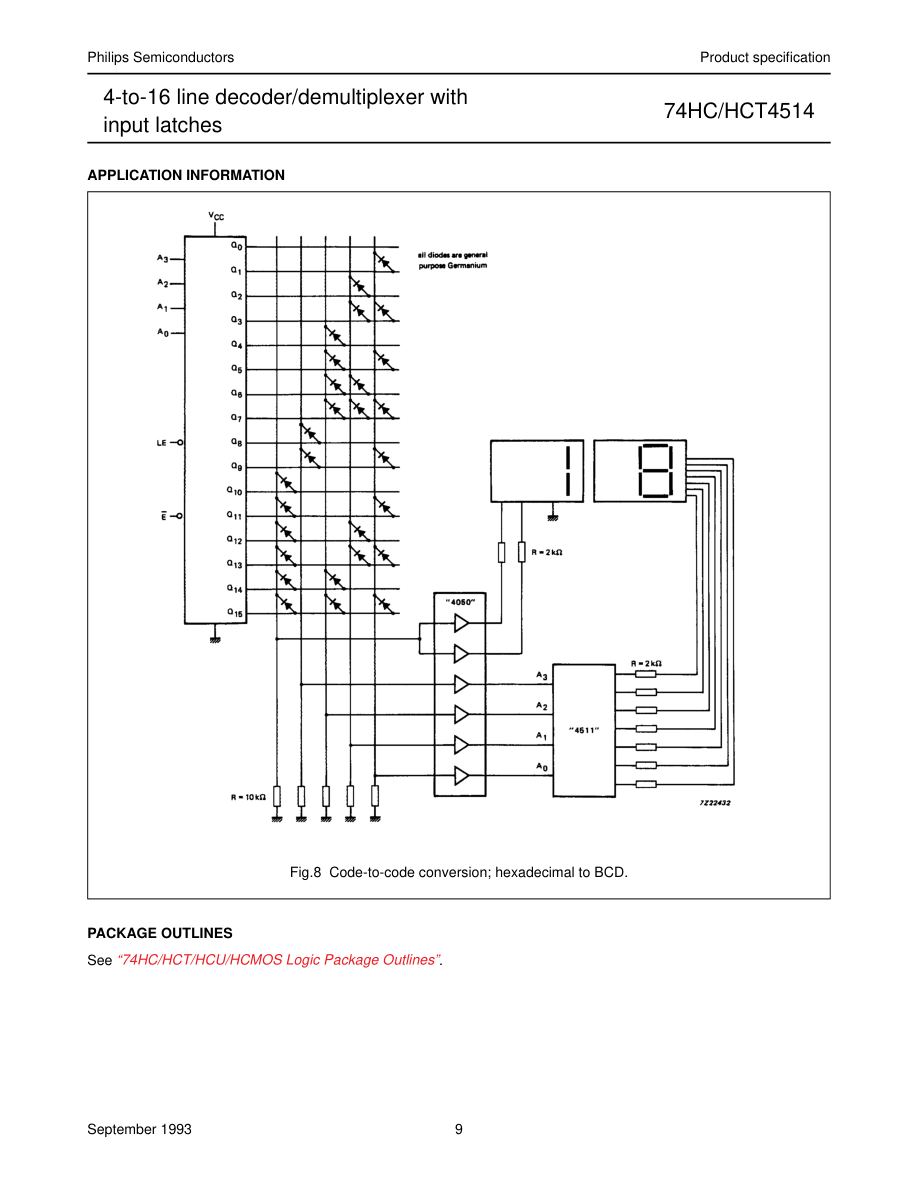
The 74HC/HCT4514 are high-speed Si-gate CMOS devices and are pin compatible with “4514” of the “4000B” series. They are specified in compliance with JEDEC standard no. 7A.
QUICK REFERENCE DATA
GND = 0 V; Tamb = 25 °C; tr = tf = 6 ns
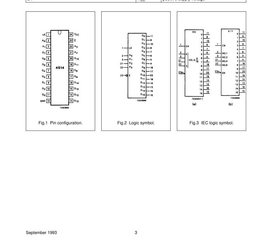
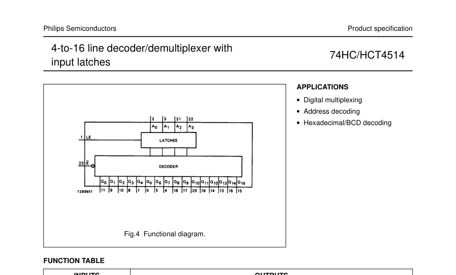
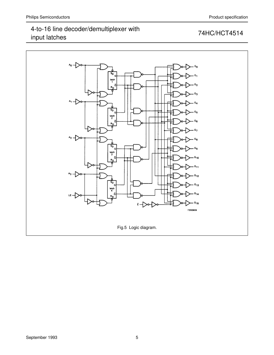
The 74HC/HCT4514 are 4-to-16 line decoders/demultiplexers having four binary weighted address inputs (A0 to A3), with latches, a latch enable input (LE), and an active LOW enable input (E). The 16 outputs (Q0 to Q15) are mutually exclusive active HIGH. When LE is HIGH, the selected output is determined by the data on An. When LE goes LOW, the last data present at An are stored in the latches and the outputs remain stable. When E is LOW, the selected output, determined by the contents of the latch, is HIGH. At E HIGH, all outputs are LOW. The enable input (E) does not affect the state of the latch. When the “4514” is used as a demultiplexer, E is the data
input and A0 to A3 are the address inputs.
| SYMBOL | PARAMETER | CONDITIONS | TYPICAL | UNIT | |
|---|---|---|---|---|---|
| HC | HCT | ||||
| t / t PHL PLH | propagation delay A to Q n n | C = 15 pF; V = 5 V L CC | 23 | 26 | ns |
| C I | input capacitance | 3.5 | 3.5 | pF | |
| C PD | power dissipation capacitance per package | notes 1 and 2 | 44 | 45 | pF |
Notes 1. CPD is used to determine the dynamic power dissipation (PD in µW): PD = CPD × VCC2 × fi +∑ (CL × VCC2 × fo) where: fi = input frequency in MHz fo = output frequency in MHz ∑ (CL × VCC2 × fo) = sum of outputs CL = output load capacitance in pF VCC = supply voltage in V 2. For HC the condition is VI = GND to VCC For HCT the condition is VI = GND to VCC − 1.5 V
ORDERING INFORMATION
See “74HC/HCT/HCU/HCMOS Logic Package Information”.
Page 3
| PIN NO. | SYMBOL | NAME AND FUNCTION |
|---|---|---|
| 1 2, 3, 21, 22 11, 9, 10, 8, 7, 6, 5, 4, 18, 17, 20, 19, 14, 13, 16, 15 12 23 24 | LE A to A 0 3 Q to Q 0 15 GND E V CC | latch enable input (active HIGH) address inputs multiplexer outputs (active HIGH) ground (0 V) enable input (active LOW) positive supply voltage |
Page 4
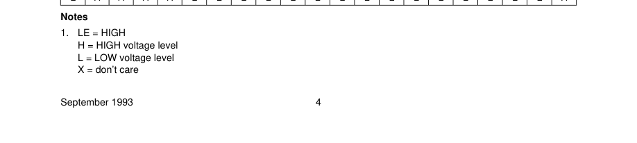
| INPUTS | OUTPUTS | |||||||||||||||||||
| E | A 0 | A 1 | A 2 | A 3 | Q 0 | Q 1 | Q 2 | Q 3 | Q 4 | Q 5 | Q 6 | Q 7 | Q 8 | Q 9 | Q 10 | Q 11 | Q 12 | Q 13 | Q 14 | Q 15 |
| H L L L L L L L L L L L L L L L L | X L H L H L H L H L H L H L H L H | X L L H H L L H H L L H H L L H H | X L L L L H H H H L L L L H H H H | X L L L L L L L L H H H H H H H H | L H L L L L L L L L L L L L L L L | L L H L L L L L L L L L L L L L L | L L L H L L L L L L L L L L L L L | L L L L H L L L L L L L L L L L L | L L L L L H L L L L L L L L L L L | L L L L L L H L L L L L L L L L L | L L L L L L L H L L L L L L L L L | L L L L L L L L H L L L L L L L L | L L L L L L L L L H L L L L L L L | L L L L L L L L L L H L L L L L L | L L L L L L L L L L L H L L L L L | L L L L L L L L L L L L H L L L L | L L L L L L L L L L L L L H L L L | L L L L L L L L L L L L L L H L L | L L L L L L L L L L L L L L L H L | L L L L L L L L L L L L L L L L H |
Page 5
Page 6
Page 7


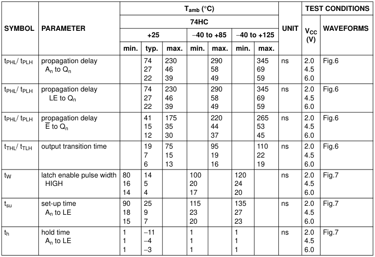
| SYMBOL | PARAMETER | T (°C) amb | UNIT | TEST CONDITIONS | |||||||
|---|---|---|---|---|---|---|---|---|---|---|---|
| 74HCT | V CC (V) | WAVEFORMS | |||||||||
| +25 | −40 to +85 | −40 to +125 | |||||||||
| min. | typ. | max. | min. | max. | min. | max. | |||||
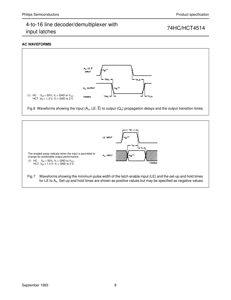
| t / t PHL PLH | propagation delay A to Q n n | 30 | 55 | 69 | 83 | ns | 4.5 | Fig.6 | |||
| t / t PHL PLH | propagation delay LE to Q n | 29 | 50 | 63 | 75 | ns | 4.5 | Fig.6 | |||
| t / t PHL PLH | propagation delay E to Q n | 17 | 40 | 50 | 60 | ns | 4.5 | Fig.6 | |||
| t / t THL TLH | output transition time | 7 | 15 | 19 | 22 | ns | 4.5 | Fig.6 | |||
| t W | latch enable pulse width HIGH | 16 | 4 | 20 | 24 | ns | 4.5 | Fig.7 | |||
| t su | set-up time A to LE n | 18 | 9 | 23 | 27 | ns | 4.5 | Fig.7 | |||
| t h | hold time A to LE n | 3 | −3 | 3 | 3 | ns | 4.5 | Fig.7 | |||
Page 8
Page 9