Download PDF
74HC4511 PHILIPS
Document overview
- PDF pages: 12
Technical content
Page 1
Page 2
FEATURES
- Latch storage of BCD inputs
- Blanking input
- Lamp test input
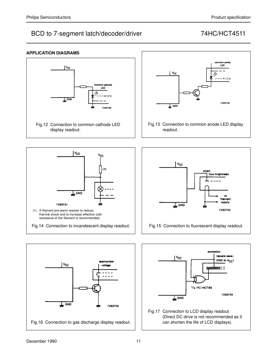
- Driving common cathode LED displays
- Guaranteed 10 mA drive capability per output
- Output capability: non-standard
- ICC category: MSI
GENERAL DESCRIPTION
The 74HC/HCT4511 are high-speed Si-gate CMOS devices and are pin compatible with “4511” of the “4000B” series. They are specified in compliance with JEDEC standard no. 7A. The 74HC/HCT4511 are BCD to 7-segment latch/decoder/drivers with four address inputs (D1 to D4), an active LOW latch enable input (LE), an active LOW
QUICK REFERENCE DATA
GND = 0 V; Tamb = 25 °C; tr = tf = 6 ns
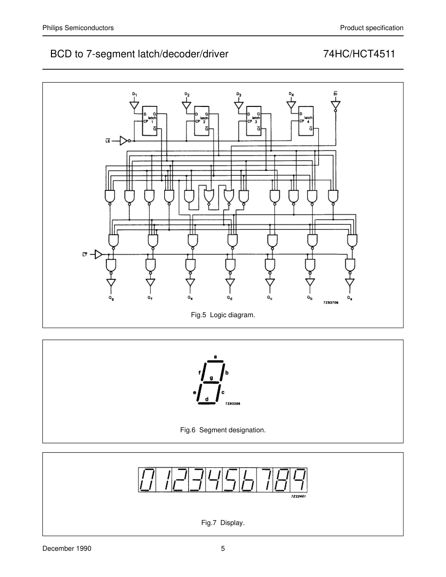
ripple blanking input (BI), an active LOW lamp test input (LT), and seven active HIGH segment outputs (Qa to Qg). When LE is LOW, the state of the segment outputs (Qa to Qg) is determined by the data on D1 to D4. When LE goes HIGH, the last data present on D1 to D4 are stored in the latches and the segment outputs remain stable. When LT is LOW, all the segment outputs are HIGH independent of all other input conditions. With LT HIGH, a LOW on BI forces all segment outputs LOW. The inputs LT and BI do not affect the latch circuit.
APPLICATIONS
- Driving LED displays
- Driving incandescent displays
- Driving fluorescent displays
- Driving LCD displays
- Driving gas discharge displays
| SYMBOL | PARAMETER | CONDITIONS | TYPICAL | UNIT | |
|---|---|---|---|---|---|
| HC | HCT | ||||
| t / t PHL PLH | propagation delay D to Q n n LE to Q n BI to Q n LT to Q n | C = 15 pF; V = 5 V L CC | 24 23 19 12 | 24 24 20 13 | ns ns ns ns |
| C I | input capacitance | 3.5 | 3.5 | pF | |
| C PD | power dissipation capacitance per latch | notes 1 and 2 | 64 | 64 | pF |
Notes 1. CPD is used to determine the dynamic power dissipation (PD in µW): PD = CPD × VCC2 × fi + ∑ (CL × VCC2 × fo) where: fi = input frequency in MHz fo = output frequency in MHz ∑ (CL × VCC2 × fo) = sum of outputs CL = output load capacitance in pF VCC = supply voltage in V 2. For HC the condition is VI = GND to VCC For HCT the condition is VI = GND to VCC − 1.5 V
Page 3
ORDERING INFORMATION
See “74HC/HCT/HCU/HCMOS Logic Package Information”.
PIN DESCRIPTION
| PIN NO. | SYMBOL | NAME AND FUNCTION |
|---|---|---|
| 3 4 5 7, 1, 2, 6 8 13, 12, 11, 10, 9, 15, 14 16 | LT BI LE D to D 1 4 GND Q to Q a g V CC | lamp test input (active LOW) ripple blanking input (active LOW) latch enable input (active LOW) BCD address inputs ground (0 V) segments outputs positive supply voltage |
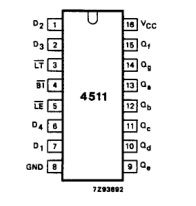
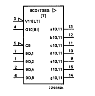
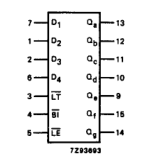
Fig.2 Logic symbol.
Fig.1 Pin configuration.
Fig.3 IEC logic symbol.
Page 4
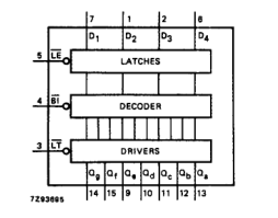
Fig.4 Functional diagram.
FUNCTION TABLE
| Column 1 | Column 2 | Column 3 | Column 4 | Column 5 | Column 6 | Column 7 | Column 8 | Column 9 | Column 10 | Column 11 | Column 12 | Column 13 | Column 14 | Column 15 |
|---|---|---|---|---|---|---|---|---|---|---|---|---|---|---|
| INPUTS | OUTPUTS | DISPLAY | ||||||||||||
| LE | BI | LT | D 4 | D 3 | D 2 | D 1 | Q a | Q b | Q c | Q d | Q e | Q f | Q g | |
| X X L L L L L L L L L L L L L L L L | X L H H H H H H H H H H H H H H H H | L H H H H H H H H H H H H H H H H H | X X L L L L L L L L H H H H H H H H | X X L L L L H H H H L L L L H H H H | X X L L H H L L H H L L H H L L H H | X X L H L H L H L H L H L H L H L H | H L H L H H L H L H H H L L L L L L | H L H H H H H L L H H H L L L L L L | H L H H L H H H H H H H L L L L L L | H L H L H H L H H L H L L L L L L L | H L H L H L L L H L H L L L L L L L | H L H L L L H H H L H H L L L L L L | H L L L H H H H H L H H L L L L L L | 8 blank 0 1 2 3 4 5 6 7 8 9 blank blank blank blank blank blank |
| H | H | H | X | X | X | X | (1) | (1) |
Note 1. Depends upon the BCD-code applied during the LOW-to-HIGH transition of LE. H = HIGH voltage level L = LOW voltage level X = don’t care
Page 5
Page 6
DC CHARACTERISTICS FOR 74HC
For the DC characteristics see “74HC/HCT/HCU/HCMOS Logic Family Specifications”. Output capability: standard, excepting VOH which is given below ICC category: MSI
Non-standard DC characteristics for 74HC Voltages are referenced to GND (ground = 0 V)
| SYMBOL | PARAMETER | T (°C) amb | UNIT | TEST CONDITIONS | ||||||||
|---|---|---|---|---|---|---|---|---|---|---|---|---|
| 74HC | V CC (V) | V I | −I O (mA) | |||||||||
| +25 | −40 to +85 | −40 to +125 | ||||||||||
| min. | typ. | max. | min. | max. | min. | max. | ||||||
| V OH | HIGH level output voltage | 3.98 3.60 | 3.84 3.35 | 3.70 3.10 | V | 4.5 | V or IH V IL | 7.5 10.0 | ||||
| V OH | HIGH level output voltage | 5.60 5.48 4.80 | 5.45 5.34 4.50 | 5.35 5.20 4.20 | V | 6.0 | V or IH V IL | 7.5 10.0 15.0 |
Page 7
AC CHARACTERISTICS FOR 74HC
GND = 0 V; tr = tf = 6 ns; CL = 50 pF
| SYMBOL | PARAMETER | T (°C) amb | UNIT | TEST CONDITIONS | |||||||
|---|---|---|---|---|---|---|---|---|---|---|---|
| 74HC | V CC (V) | WAVEFORMS | |||||||||
| +25 | −40 to +85 | −40 to +125 | |||||||||
| min. | typ. | max. | min. | max. | min. | max. | |||||
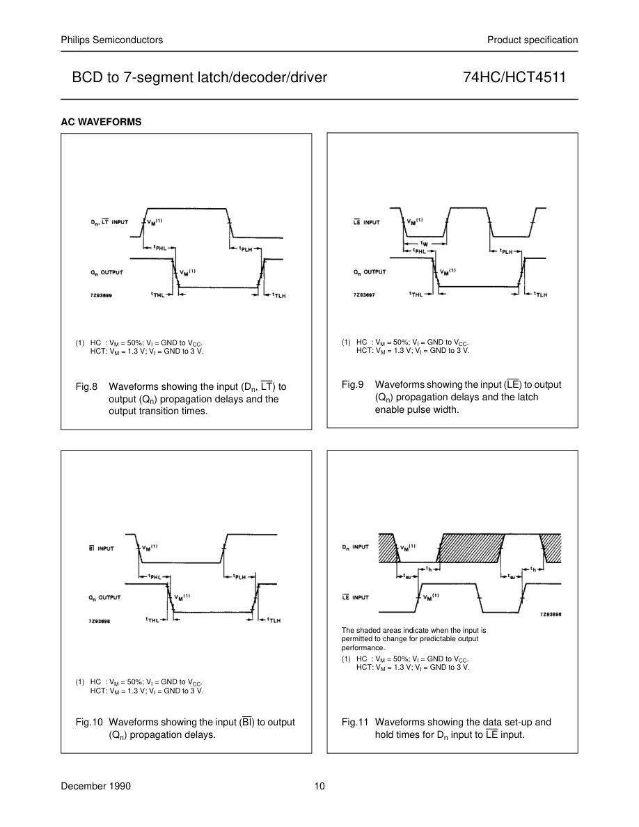
| t / t PHL PLH | propagation delay D to Q n n | 77 28 22 | 300 60 51 | 375 75 64 | 450 90 77 | ns | 2.0 4.5 6.0 | Fig.8 | |||
| t / t PHL PLH | propagation delay LE to Q n | 74 27 22 | 270 54 46 | 330 68 58 | 405 81 69 | ns | 2.0 4.5 6.0 | Fig.9 | |||
| t / t PHL PLH | propagation delay BI to Q n | 61 22 18 | 220 44 37 | 275 55 47 | 330 66 56 | ns | 2.0 4.5 6.0 | Fig.10 | |||
| t / t PHL PLH | propagation delay LT to Q n | 41 15 12 | 150 30 26 | 190 38 33 | 225 45 38 | ns | 2.0 4.5 6.0 | Fig.8 | |||
| t / t THL TLH | output transition time | 19 7 6 | 75 15 13 | 95 19 16 | 110 22 19 | ns | 2.0 4.5 6.0 | Figs 8, 9 and 10 | |||
| t W | latch enable pulse width LOW | 80 16 14 | 11 4 3 | 100 20 17 | 120 24 20 | ns | 2.0 4.5 6.0 | Fig.9 | |||
| t su | set-up time D to LE n | 60 12 10 | 14 5 4 | 75 15 13 | 90 18 15 | ns | 2.0 4.5 6.0 | Fig.11 | |||
| t h | hold time D to LE n | 0 0 0 | −11 −4 −3 | 0 0 0 | 0 0 0 | ns | 2.0 4.5 6.0 | Fig.11 |
Page 8
DC CHARACTERISTICS FOR 74HCT
For the DC characteristics see “74HC/HCT/HCU/HCMOS Logic Family Specifications”. Output capability: standard, excepting VOH which is given below ICC category: MSI
Non-standard DC characteristics for 74HCT Voltages are referenced to GND (ground = 0 V)
SYMBOL
PARAMETER
+25 min. typ. max.
HIGH level output voltage 3.98 VOH
3.60
Note to HCT types
Tamb (°C)
TEST
CONDITIONS
74HCT
UNIT
VCC VI
−IO
−40 to +85 −40 to +125
(V)
(mA)
min. max. min. max. 3.84
3.70
V 4.5 VIH or 7.5
3.35
3.10
VIL 10.0
The value of additional quiescent supply current (∆ICC) for a unit load of 1 is given in the family specifications. To determine ∆ICC per input, multiply this value by the unit load coefficient shown in the table below.
| INPUT | UNIT LOAD COEFFICIENT |
|---|---|
| LT, LE BI, D n | 1.50 0.30 |
Page 9
AC CHARACTERISTICS FOR 74HCT
GND = 0 V; tr = tf = 6 ns; CL = 50 pF
| SYMBOL | PARAMETER | T (°C) amb | UNIT | TEST CONDITIONS | |||||||
|---|---|---|---|---|---|---|---|---|---|---|---|
| 74HCT | V CC (V) | WAVEFORMS | |||||||||
| +25 | −40 to +85 | −40 to +125 | |||||||||
| min. | typ. | max. | min. | max. | min. | max. | |||||
| t / t PHL PLH | propagation delay D to Q n n | 28 | 60 | 75 | 90 | ns | 4.5 | Fig.8 | |||
| t / t PHL PLH | propagation delay LE to Q n | 27 | 54 | 68 | 81 | ns | 4.5 | Fig.9 | |||
| t / t PHL PLH | propagation delay BI to Q n | 23 | 44 | 55 | 66 | ns | 4.5 | Fig.10 | |||
| t / t PHL PLH | propagation delay LT to Q n | 16 | 30 | 38 | 45 | ns | 4.5 | Fig.8 | |||
| t / t THL TLH | output transition time | 7 | 15 | 19 | 22 | ns | 4.5 | Figs 8, 9 and 10 | |||
| t W | latch enable pulse width LOW | 16 | 5 | 20 | 24 | ns | 4.5 | Fig.9 | |||
| t su | set-up time D to LE n | 12 | 5 | 15 | 18 | ns | 4.5 | Fig.11 | |||
| t h | hold time D to LE n | 0 | −4 | 0 | 0 | ns | 4.5 | Fig.11 |
Page 10
Page 11
Page 12