Download PDF
74HC4351 PHILIPS
Document overview
- PDF pages: 17
Technical content
Page 1
Page 2
8-channel analog
multiplexer/demultiplexer with latch
FEATURES
- Wide analog input voltage range: ± 5 V
- Low “ON” resistance: 80 Ω (typ.) at VCC − VEE = 4.5 V 70 Ω (typ.) at VCC − VEE = 6.0 V 60 Ω (typ.) at VCC − VEE = 9.0 V
- Logic level translation: to enable 5 V logic to communicate with ± 5 V analog signals
- Typical “break before make” built in
- Address latches provided
- Output capability: non-standard
- ICC category: MSI
GENERAL DESCRIPTION
The 74HC/HCT4351 are high-speed Si-gate CMOS devices. They are specified in compliance with JEDEC standard no. 7A.
QUICK REFERENCE DATA
VEE = GND = 0 V; Tamb = 25 °C; tr = tf = 6 ns
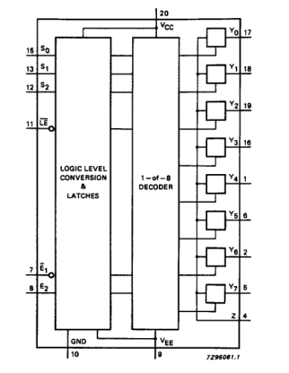
The 74HC/HCT4351 are 8-channel analog multiplexers/demultiplexers with three select inputs (S0 to S2), two enable inputs (E1 and E2), a latch enable input (LE), eight independent inputs/outputs (Y0 to Y7) and a common input/output (Z). With E1 LOW and E2 is HIGH, one of the eight switches is selected (low impedance ON-state) by S0 to S2. The data at the select inputs may be latched by using the active LOW latch enable input (LE). When LE is HIGH the latch is transparent. When either of the two enable inputs, E1 (active LOW) and E2 (active HIGH), is inactive, all 8 analog switches are turned off. VCC and GND are the supply voltage pins for the digital control inputs (S0 to S2, LE, E1 and E2). The VCC to GND
ranges are 2.0 to 10.0 V for HC and 4.5 to 5.5 V for HCT. The analog inputs/outputs (Y0 to Y7, and Z) can swing between VCC as a positive limit and VEE as a negative limit. VCC − VEE may not exceed 10.0 V. For operation as a digital multiplexer/demultiplexer, VEE is connected to GND (typically ground).
| SYMBOL | PARAMETER | CONDITIONS | TYPICAL | UNIT | |
|---|---|---|---|---|---|
| HC | HCT | ||||
| t / t PZH PZL | turn “ON” time E 1, E or S to V 2 n os | C = 15 pF; R = 1 kΩ; V = 5 V L L CC | 27 | 35 | ns |
| t / t PHZ PLZ | turn “OFF” time E 1, E or S to V 2 n os | 21 | 23 | ns | |
| C I | input capacitance | 3.5 | 3.5 | pF | |
| C PD | power dissipation capacitance per switch | notes 1 and 2 | 25 | 25 | pF |
| C S | max. switch capacitance independent (Y) common (Z) | 5 25 | 5 25 | pF pF |
Notes 1. CPD is used to determine the dynamic power dissipation (PD in µW): PD = CPD × VCC2 × fi +∑ {(CL+ CS) × VCC2 × fo} where: fi = input frequency in MHz fo = output frequency in MHz CL = output load capacitance in pF CS = max. switch capacitance in pF ∑ {(CL+ CS) × VCC2 × fo} = sum of outputs VCC = supply voltage in V
- For HC the condition is VI = GND to VCC For HCT the condition is VI = GND to VCC − 1.5 V
ORDERING INFORMATION
See “74HC/HCT/HCU/HCMOS Logic Package Information”.
Page 3
PIN DESCRIPTION
| PIN NO. | SYMBOL | NAME AND FUNCTION |
|---|---|---|
| 4 3, 14 7 8 9 10 11 15, 13, 12 17, 18, 19, 16, 1, 6, 2, 5 20 | Z n.c. E 1 E 2 V EE GND LE S to S 0 2 Y to Y 0 7 V CC | common not connected enable input (active LOW) enable input (active HIGH) negative supply voltage ground (0 V) latch enable input (active LOW) select inputs independent inputs/outputs positive supply voltage |
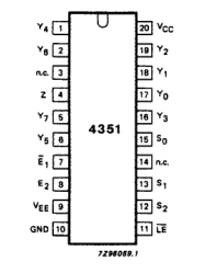
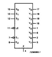
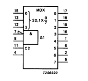
Fig.1 Pin configuration.
Fig.2
Fig.3 IEC logic symbol.
Page 4
FUNCTION TABLE
| Column 1 | Column 2 | Column 3 | Column 4 | Column 5 | Column 6 | Column 7 |
|---|---|---|---|---|---|---|
| INPUTS | CHANNEL ON | |||||
| E 1 | E 2 | LE | S 2 | S 1 | S 0 | |
| H X L L L L L L L L L X | X L H H H H H H H H H X | X X H H H H H H H H L ↓ | X X L L L L H H H H X X | X X L L H H L L H H X X | X X L H L H L H L H X X | none none Y 0 Y 1 Y 2 Y 3 Y 4 Y 5 Y 6 Y 7 (1) (2) |
Notes 1. Last selected channel “ON”. 2. Selected channels latched. 3. H = HIGH voltage level L = LOW voltage level X = don’t care ↓ = HIGH-to-LOW LE transition
APPLICATIONS
- Analog multiplexing and demultiplexing
- Digital multiplexing and demultiplexing
- Signal gating
Fig.4 Functional diagram.
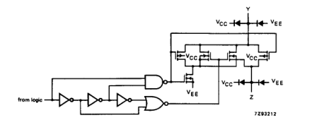
Fig.5 Schematic diagram (one switch).
Page 5
RATINGS
Limiting values in accordance with the Absolute Maximum System (IEC 134) Voltages are referenced to VEE = GND (ground = 0 V)
| SYMBOL | PARAMETER | MIN. | MAX. | UNIT | CONDITIONS |
|---|---|---|---|---|---|
| V CC | DC supply voltage | −0.5 | +11.0 | V | |
| ±I IK | DC digital input diode current | 20 | mA | for V < −0.5 V or V > V + 0.5 V I I CC | |
| ±I SK | DC switch diode current | 20 | mA | for V < −0.5 V or V > V + 0.5 V S S CC | |
| ±I S | DC switch current | 25 | mA | for −0.5 V < V < V + 0.5 V S CC | |
| ±I EE | DC V current EE | 20 | mA | ||
| ±I ±I CC; GND | DC V or GND current CC | 50 | mA | ||
| T stg | storage temperature range | −65 | +150 | °C | |
| P tot | power dissipation per package plastic DIL | 750 | mW | for temperature range: −40 to +125 °C 74HC/HCT above +70 °C: derate linearly with 12 mW/K | |
| plastic mini-pack (SO) | 500 | mW | above +70 °C: derate linearly with 8 mW/K | ||
| P S | power dissipation per switch | 100 | mW |
Note to ratings 1. To avoid drawing VCC current out of terminal Z, when switch current flows in terminals Yn, the voltage drop across the bidirectional switch must not exceed 0.4 V. If the switch current flows into terminal Z, no VCC current will flow out of terminals Yn. In this case there is no limit for the voltage drop across the switch, but the voltages at Yn and Z may not exceed VCC or VEE.
RECOMMENDED OPERATING CONDITIONS
| SYMBOL | PARAMETER | 74HC | 74HCT | UNIT | CONDITIONS | ||||
|---|---|---|---|---|---|---|---|---|---|
| min. | typ. | max. | min. | typ. | max. | ||||
| V CC | DC supply voltage V −GND CC | 2.0 | 5.0 | 10.0 | 4.5 | 5.0 | 5.5 | V | see Figs 6 and 7 |
| V CC | DC supply voltage V −V CC EE | 2.0 | 5.0 | 10.0 | 2.0 | 5.0 | 10.0 | V | see Figs 6 and 7 |
| V I | DC input voltage range | GND | V CC | GND | V CC | V | |||
| V S | DC switch voltage range | V EE | V CC | V EE | V CC | V | |||
| T amb | operating ambient temperature range | −40 | +85 | −40 | +85 | °C | see DC and AC CHARACTERISTICS | ||
| T amb | operating ambient temperature range | −40 | +125 | −40 | +125 | °C | |||
| t, t r f | input rise and fall times | 6.0 | 1000 500 400 250 | 6.0 | 500 | ns | V = 2.0 V CC V = 4.5 V CC V = 6.0 V CC V = 10.0 V CC |
Page 6
MBA334
10 handbook, halfpage VCC - GND (V) 8
operating area
6
4
2
0 0 2 4 6 8 10 VCC- VEE (V)
Fig.6 Guaranteed operating area as a function of the supply voltages for 74HC4351.
DC CHARACTERISTICS FOR 74HC/HCT
For 74HC: VCC − GND or VCC − VEE = 2.0, 4.5, 6.0 and 9.0 V
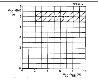
Fig.7 Guaranteed operating area as a function of the supply voltages for 74HCT4351.
For 74HCT: VCC − GND = 4.5 and 5.5 V; VCC − VEE = 2.0, 4.5, 6.0 and 9.0 V
| SYMBOL | PARAMETER | T (°C) amb | UNIT | TEST CONDITIONS | ||||||||||
|---|---|---|---|---|---|---|---|---|---|---|---|---|---|---|
| 74HC/HCT | V CC (V) | V EE (V) | I S (µA) | V is | V I | |||||||||
| +25 | −40 to +85 | −40 to +125 | ||||||||||||
| min. | typ. | max. | min. | max. | min. | max. | ||||||||
| R ON | ON resistance (rail) | − 100 90 70 | − 180 160 130 | − 225 200 165 | − 270 240 195 | Ω Ω Ω Ω | 2.0 4.5 6.0 4.5 | 0 0 0 −4.5 | 100 1000 1000 1000 | V CC to V EE | V IN or V IL | |||
| R ON | ON resistance (rail) | 150 80 70 60 | − 140 120 105 | − 175 150 130 | − 210 180 160 | Ω Ω Ω Ω | 2.0 4.5 6.0 4.5 | 0 0 0 −4.5 | 100 1000 1000 1000 | V EE | V IH or V IL | |||
| R ON | ON resistance (rail) | 150 90 80 65 | − 160 140 120 | − 200 175 150 | − 240 210 180 | Ω Ω Ω Ω | 2.0 4.5 6.0 4.5 | 0 0 0 −4.5 | 100 1000 1000 1000 | V CC | V IH or V IL | |||
| ∆R ON | maximum ∆ON resistance between any two channels | − 9 8 6 | Ω Ω Ω Ω | 2.0 4.5 6.0 4.5 | 0 0 0 −4.5 | V CC to V EE | V IH or V IL |
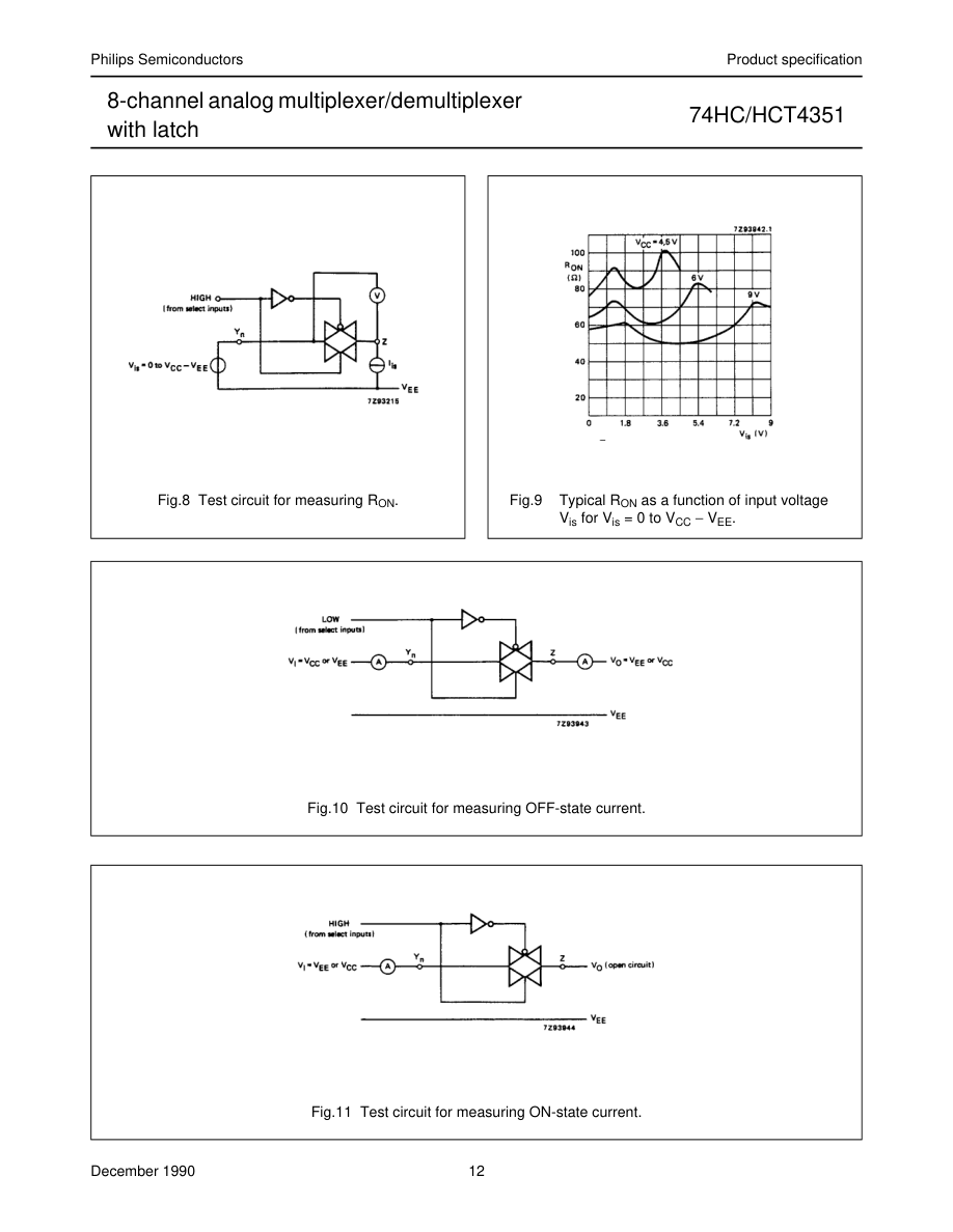
Notes to DC characteristics 1. At supply voltages (VCC − VEE) approaching 2.0 V, the analog switch ON-resistance becomes extremely non-linear. There it is recommended that these devices be used to transmit digital signals only, when using these supply voltages. 2. For test circuit measuring RON see Fig.8.
Page 7
DC CHARACTERISTICS FOR 74HC
Voltages are referenced to GND (ground = 0 V)
| SYMBOL | PARAMETER | T (°C) amb | UNIT | TEST CONDITIONS | |||||||||
|---|---|---|---|---|---|---|---|---|---|---|---|---|---|
| 74HC | V CC (V) | V EE (V) | V I | OTHER | |||||||||
| +25 | −40 to +85 | −40 to +125 | |||||||||||
| min. | typ. | max. | min. | max. | min. | max. | |||||||
| V IH | HIGH level input voltage | 1.5 3.15 4.2 6.3 | 1.2 2.4 3.2 4.7 | 1.5 3.15 4.2 6.3 | 1.5 3.15 4.2 6.3 | V | 2.0 4.5 6.0 9.0 | ||||||
| V IL | LOW level input voltage | 0.8 2.1 2.8 4.3 | 0.5 1.35 1.8 2.7 | 0.5 1.35 1.8 2.7 | 0.5 1.35 1.8 2.7 | V | 2.0 4.5 6.0 9.0 | ||||||
| ±I I | input leakage current | 0.1 0.2 | 1.0 2.0 | 1.0 2.0 | µA | 6.0 10.0 | 0 0 | V CC or GND | |||||
| ±I S | analog switch OFF-state current per channel | 0.1 | 1.0 | 1.0 | µA | 10.0 | 0 | V IH or V IL | V = S V −V CC EE (see Fig.10) | ||||
| ±I S | analog switch OFF-state current all channels | 0.4 | 4.0 | 4.0 | µA | 10.0 | 0 | V IH or V IL | V = S V −V CC EE (see Fig.10) | ||||
| ±I S | analog switch ON-state current | 0.4 | 4.0 | 4.0 | µA | 10.0 | 0 | V IH or V IL | V = S V −V CC EE (see Fig.11) | ||||
| I CC | quiescent supply current | 8.0 16.0 | 80.0 160.0 | 160.0 320.0 | µA | 6.0 10.0 | 0 0 | V CC or GND | V = V is EE or V ; CC V = V os CC or V EE |
Page 8
AC CHARACTERISTICS FOR 74HC
GND = 0 V; tr = tf = 6 ns; CL = 50 pF
| SYMBOL | PARAMETER | T (°C) amb | UNIT | TEST CONDITIONS | ||||||||
|---|---|---|---|---|---|---|---|---|---|---|---|---|
| 74HC | V CC (V) | V EE (V) | OTHER | |||||||||
| +25 | −40 to +85 | −40 to +125 | ||||||||||
| min. | typ. | max. | min. | max. | min. | max. | ||||||
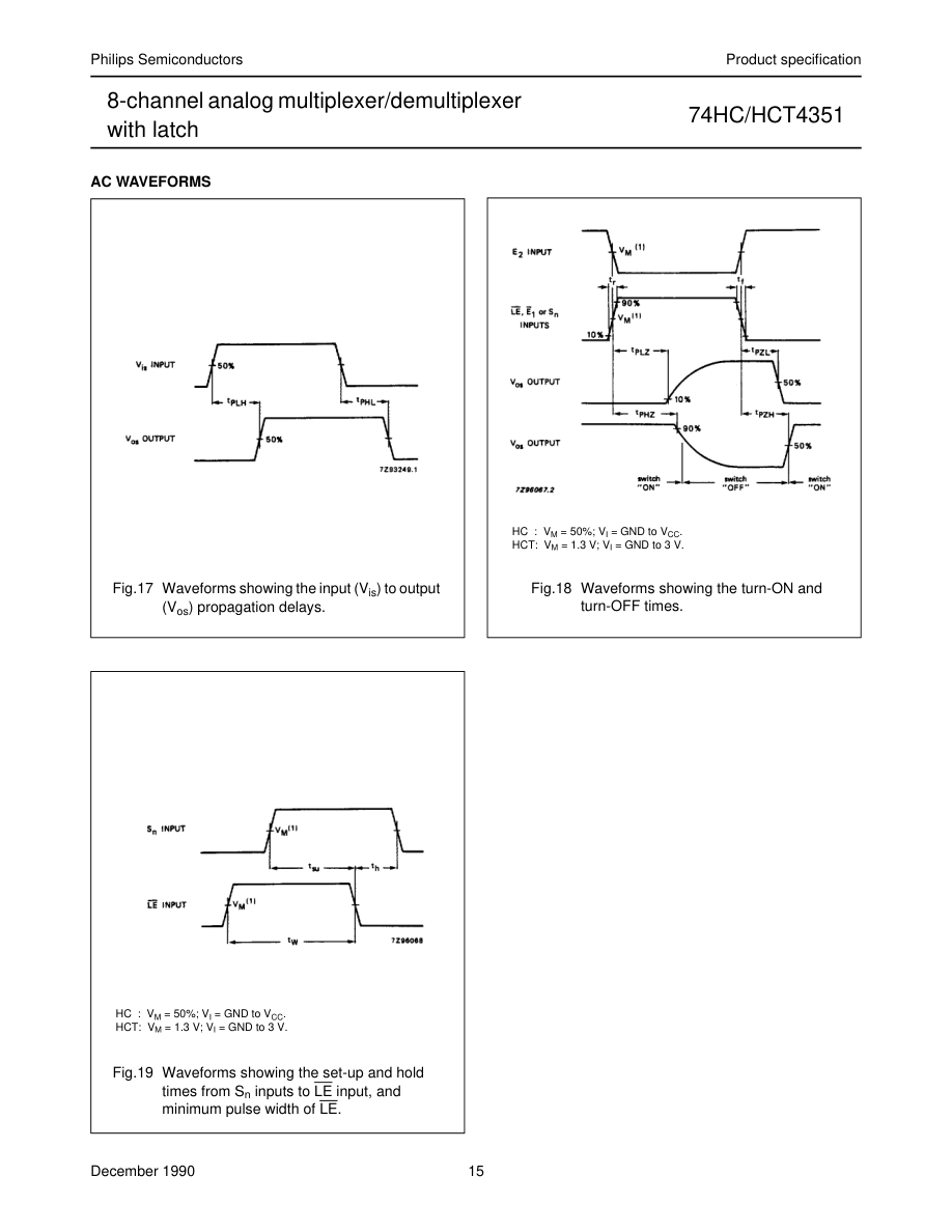
| t / t PHL PLH | propagation delay V to V is os | 14 5 4 4 | 60 12 10 8 | 75 15 13 10 | 90 18 15 12 | ns | 2.0 4.5 6.0 4.5 | 0 0 0 −4.5 | R = ∞; L C = 50 pF L (see Fig.17) | |||
| t / t PZH PZL | turn “ON” time E to V 1 os | 85 31 25 28 | 300 60 51 55 | 375 75 64 69 | 450 90 77 83 | ns | 2.0 4.5 6.0 4.5 | 0 0 0 −4.5 | R = 1 kΩ; L C = 50 pF L (see Fig.18) | |||
| t / t PZH PZL | turn “ON” time E to V 2 os | 85 31 25 25 | 300 60 51 55 | 375 75 64 69 | 450 90 77 83 | ns | 2.0 4.5 6.0 4.5 | 0 0 0 −4.5 | R = 1 kΩ; L C = 50 pF L (see Fig.18) | |||
| t / t PZH PZL | turn “ON” time LE to V os | 91 33 26 27 | 300 60 51 55 | 375 75 64 69 | 450 90 77 83 | ns | 2.0 4.5 6.0 4.5 | 0 0 0 −4.5 | R = 1 kΩ; L C = 50 pF L (see Fig.18) | |||
| t / t PZH PZL | turn “ON” time S to V n os | 88 32 26 25 | 300 60 51 50 | 375 75 64 63 | 450 90 77 75 | ns | 2.0 4.5 6.0 4.5 | 0 0 0 −4.5 | R = 1 kΩ; L C = 50 pF L (see Fig.18) | |||
| t / t PHZ PLZ | turn “OFF” time E to V 1 os | 69 25 20 20 | 250 50 43 40 | 315 63 54 50 | 375 75 64 60 | ns | 2.0 4.5 6.0 4.5 | 0 0 0 −4.5 | R = 1 kΩ; L C = 50 pF L (see Fig.18) | |||
| t / t PHZ PLZ | turn “OFF” time E to V 2 os | 72 26 21 19 | 250 50 43 40 | 315 63 54 50 | 375 75 64 60 | ns | 2.0 4.5 6.0 4.5 | 0 0 0 −4.5 | R = 1 kΩ; L C = 50 pF L (see Fig.18) | |||
| t / t PHZ PLZ | turn “OFF” time LE to V os | 83 30 24 26 | 275 55 47 45 | 345 69 59 56 | 415 83 71 68 | ns | 2.0 4.5 6.0 4.5 | 0 0 0 −4.5 | R = 1 kΩ; L C = 50 pF L (see Fig.18) | |||
| t / t PHZ PLZ | turn “OFF” time S to V n os | 80 29 23 24 | 275 55 47 48 | 345 69 59 60 | 415 83 71 72 | ns | 2.0 4.5 6.0 4.5 | 0 0 0 −4.5 | R = 1 kΩ; L C = 50 pF L (see Fig.18) |
Page 9
| SYMBOL | PARAMETER | T (°C) amb | UNIT | TEST CONDITIONS | ||||||||
|---|---|---|---|---|---|---|---|---|---|---|---|---|
| 74HC | V CC (V) | V EE (V) | OTHER | |||||||||
| +25 | −40 to +85 | −40 to +125 | ||||||||||
| min. | typ. | max. | min. | max. | min. | max. | ||||||
| t su | set-up time S to LE n | 60 12 10 18 | 17 6 5 9 | 75 15 13 23 | 90 18 15 27 | ns | 2.0 4.5 6.0 4.5 | 0 0 0 −4.5 | R = 1 kΩ; L C = 50 pF L (see Fig.19) | |||
| t h | hold time S to LE n | 5 5 5 5 | −8 −3 −2 −4 | 5 5 5 5 | 5 5 5 5 | ns | 2.0 4.5 6.0 4.5 | 0 0 0 −4.5 | R = 1 kΩ; L C = 50 pF L (see Fig.19) | |||
| t W | LE minimum pulse width HIGH | 100 20 17 25 | 11 1 3 7 | 125 25 21 31 | 150 30 26 38 | ns | 2.0 4.5 6.0 4.5 | 0 0 0 −4.5 | R = 1 kΩ; L C = 50 pF L (see Fig.19) |
Page 10
DC CHARACTERISTICS FOR 74HCT
Voltages are referenced to GND (ground = 0)
| SYMBOL | PARAMETER | T (°C) amb | UNIT | TEST CONDITIONS | |||||||||
|---|---|---|---|---|---|---|---|---|---|---|---|---|---|
| 74HCT | V CC (V) | V EE (V) | V I | OTHER | |||||||||
| +25 | −40 to +85 | −40 to +125 | |||||||||||
| min. | typ. | max. | min. | max. | min. | max. | |||||||
| V IH | HIGH level input voltage | 2.0 | 1.6 | 2.0 | 2.0 | V | 4.5 to 5.5 | ||||||
| V IL | LOW level input voltage | 1.2 | 0.8 | 0.8 | 0.8 | V | 4.5 to 5.5 | ||||||
| ±I I | input leakage current | 0.1 | 1.0 | 1.0 | µA | 5.5 | 0 | V CC or GND | |||||
| ±I S | analog switch OFF-state current per channel | 0.1 | 1.0 | 1.0 | µA | 10.0 | 0 | V IH or V IL | V = S V −V CC EE (see Fig.10) | ||||
| ±I S | analog switch OFF-state current all channels | 0.4 | 4.0 | 4.0 | µA | 10.0 | 0 | V IH or V IL | V = S V −V CC EE (see Fig.10) | ||||
| ±I S | analog switch ON-state current | 0.4 | 4.0 | 4.0 | µA | 10.0 | 0 | V IH or V IL | V = S V −V CC EE (see Fig.11) | ||||
| I CC | quiescent supply current | 8.0 16.0 | 80.0 160.0 | 160.0 320.0 | µA | 5.5 5.0 | 0 −5.0 | V CC or GND | V = V is EE or V ; CC V = V os CC or V EE | ||||
| ∆I CC | additional quiescent supply current per input pin for unit load coefficient is 1 (note 1) | 100 | 360 | 450 | 490 | µA | 4.5 to 5.5 | 0 | V CC −2.1 V | other inputs at V or CC GND |
Note to HCT types 1. The value of additional quiescent supply current (∆ICC) for a unit load of 1 is given here. To determine ∆ICC per input, multiply this value by the unit load coefficient shown in the table below.
| INPUT | UNIT LOAD COEFFICIENT |
|---|---|
| E , E 1 2 S n LE | 0.50 0.50 1.5 |
Page 11
AC CHARACTERISTICS FOR 74HCT
GND = 0 V; tr = tf = 6 ns; CL = 50 pF
| SYMBOL | PARAMETER | T (°C) amb | UNIT | TEST CONDITIONS | ||||||||
|---|---|---|---|---|---|---|---|---|---|---|---|---|
| 74HCT | V CC (V) | V EE (V) | OTHER | |||||||||
| +25 | −40 to +85 | −40 to +125 | ||||||||||
| min. | typ. | max. | min. | max. | min. | max. | ||||||
| t / t PHL PLH | propagation delay V to V is os | 6 4 | 12 8 | 15 10 | 18 12 | ns | 4.5 4.5 | 0 −4.5 | R = ∞; L C = 50 pF L (see Fig.17) | |||
| t / t PZH PZL | turn “ON” time E to V 1 os | 40 31 | 75 60 | 94 75 | 113 90 | ns | 4.5 4.5 | 0 −4.5 | R = 1 kΩ; L C = 50 pF L (see Fig.18) | |||
| t / t PZH PZL | turn “ON” time E to V 2 os | 35 26 | 70 50 | 88 63 | 105 75 | ns | 4.5 4.5 | 0 −4.5 | R = 1 kΩ; L C = 50 pF L (see Fig.18) | |||
| t / t PZH PZL | turn “ON” time LE to V os | 42 37 | 75 60 | 94 75 | 113 90 | ns | 4.5 4.5 | 0 −4.5 | R = 1 kΩ; L C = 50 pF L (see Fig.18) | |||
| t / t PZH PZL | turn “ON” time S to V n os | 39 30 | 75 60 | 94 75 | 113 90 | ns | 4.5 4.5 | 0 −4.5 | R = 1 kΩ; L C = 50 pF L (see Fig.18) | |||
| t / t PHZ PLZ | turn “OFF” time E to V 1 os | 27 20 | 55 40 | 69 50 | 83 60 | ns | 4.5 4.5 | 0 −4.5 | R = 1 kΩ; L C = 50 pF L (see Fig.18) | |||
| t / t PHZ PLZ | turn “OFF” time E to V 2 os | 32 26 | 60 50 | 75 63 | 90 75 | ns | 4.5 4.5 | 0 −4.5 | R = 1 kΩ; L C = 50 pF L (see Fig.18) | |||
| t / t PHZ PLZ | turn “OFF” time LE to V os | 33 30 | 60 55 | 75 69 | 90 83 | ns | 4.5 4.5 | 0 −4.5 | R = 1 kΩ; L C = 50 pF L (see Fig.18) | |||
| t / t PHZ PLZ | turn “OFF” time S to V n os | 33 29 | 65 55 | 81 69 | 98 83 | ns | 4.5 4.5 | 0 −4.5 | R = 1 kΩ; L C = 50 pF L (see Fig.18) | |||
| t su | set-up time S to LE n | 12 14 | 6 7 | 15 18 | 18 21 | ns | 4.5 4.5 | 0 −4.5 | R = 1 kΩ; L C = 50 pF L (see Fig.19) | |||
| t h | hold time S to LE n | 5 5 | −1 −2 | 5 5 | 5 5 | ns | 4.5 4.5 | 0 −4.5 | R = 1 kΩ; L C = 50 pF L (see Fig.19) | |||
| t W | LE minimum pulse width HIGH | 25 25 | 13 13 | 31 31 | 38 38 | ns | 4.5 4.5 | 0 −4.5 | R = 1 kΩ; L C = 50 pF L (see Fig.19) |
Page 12
Page 13
ADDITIONAL AC CHARACTERISTICS FOR 74HC/HCT
Recommended conditions and typical values GND = 0 V; Tamb = 25 °C
| SYMBOL | PARAMETER | typ. | UNIT | V CC (V) | V EE (V) | V is(p−p) (V) | CONDITIONS |
|---|---|---|---|---|---|---|---|
| sine-wave distortion f = 1 kHz | 0.04 0.02 | % % | 2.25 4.5 | −2.25 −4.5 | 4.0 8.0 | R = 10 kΩ; C = 50 pF L L (see Fig.14) | |
| sine-wave distortion f = 10 kHz | 0.12 0.06 | % % | 2.25 4.5 | −2.25 −4.5 | 4.0 8.0 | R = 10 kΩ; C = 50 pF L L (see Fig.14) | |
| switch “OFF” signal feed-through | −50 −50 | dB dB | 2.25 4.5 | −2.25 −4.5 | note 1 | R = 600 Ω; C = 50 pF L L (see Figs 12 and 15) | |
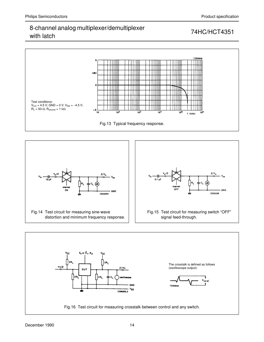
| V (p−p) | crosstalk voltage between control and any switch (peak-to-peak value) | 120 220 | mV mV | 4.5 4.5 | 0 −4.5 | R = 600 Ω; C = 50 pF; L L f = 1 MHz (E 1, E or S n, 2 square-wave between V CC and GND, t = t = 6 ns) r f (see Fig.16) | |
| f max | minimum frequency response (−3dB) | 160 170 | MHz MHz | 2.25 4.5 | −2.25 −4.5 | note 2 | R = 50 Ω; C = 10 pF L L (see Figs 13 and 14) |
| C S | maximum switch capacitance independent (Y) common (Z) | 5 25 | pF pF |
Notes to AC characteristics 1. Adjust input voltage Vis to 0 dBm level (0 dBm = 1 mW into 600 Ω). 2. Adjust input voltage Vis to 0 dBm level at Vos for 1 MHz (0 dBm = 1 mW into 50 Ω).
Vis is the input voltage at a Yn or Z terminal, whichever is assigned as an input. Vos is the output voltage at a Yn or Z terminal, whichever is assigned as an output.
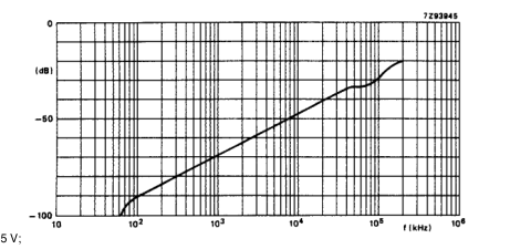
Test conditions: VCC = 4.5 V; GND = 0 V; VEE = −4.5 V; RL = 50 Ω; Rsource = 1 kΩ.
Fig.12 Typical switch “OFF” signal feed-through as a function of frequency.
Page 14
Page 15
Page 16
TEST CIRCUIT AND WAVEFORMS
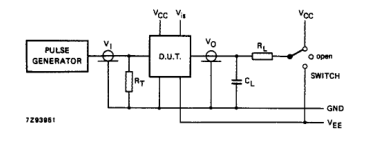
Conditions
| Column 1 | Column 2 | Column 3 |
|---|---|---|
| TEST | SWITCH | V is |
| t PZH | V EE | V CC |
| t PZL | V CC | V EE |
| t PHZ | V EE | V CC |
| t PLZ | V CC | V EE |
| others | open | pulse |
| Column 1 | Column 2 | Column 3 | Column 4 | Column 5 |
|---|---|---|---|---|
| FAMILY | AMPLITUDE | V M | t; t r f | |
| f ; max PULSE WIDTH | OTHER | |||
| 74HC | V CC | 50% | < 2 ns | 6 ns |
| 74HCT | 3.0 V | 1.3 V | < 2 ns | 6 ns |
= load capacitance including jig and probe capacitance (see AC CHARACTERISTICS for values). CL termination resistance should be equal to the output impedance ZO of the pulse generator. RT = tf = 6 ns; when measuring fmax, there is no constraint on tr, tf with 50% duty factor. tr =
Fig.20 Test circuit for measuring AC performance.
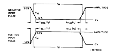
Conditions
| Column 1 | Column 2 | Column 3 |
|---|---|---|
| TEST | SWITCH | V is |
| t PZH | V EE | V CC |
| t PZL | V CC | V EE |
| t PHZ | V EE | V CC |
| t PLZ | V CC | V EE |
| others | open | pulse |
| Column 1 | Column 2 | Column 3 | Column 4 | Column 5 |
|---|---|---|---|---|
| FAMILY | AMPLITUDE | V M | t; t r f | |
| f ; max PULSE WIDTH | OTHER | |||
| 74HC | V CC | 50% | < 2 ns | 6 ns |
| 74HCT | 3.0 V | 1.3 V | < 2 ns | 6 ns |
= load capacitance including jig and probe capacitance (see AC CHARACTERISTICS for values). CL termination resistance should be equal to the output impedance ZO of the pulse generator. = RT tf = 6 ns; when measuring fmax, there is no constraint on tr, tf with 50% duty factor. tr =
Fig.21 Input pulse definitions.
Page 17