74HC40104 PHILIPS
Document overview
- PDF pages: 8
Technical content
Page 1
Page 2
4-bit bidirectional universal shift
register; 3-state
FEATURES
- Synchronous parallel or serial operating
- 3-state outputs
- Output capability: bus driver
- ICC category: MSI
GENERAL DESCRIPTION
The 74HC/HCT40104 are high-speed Si-gate CMOS devices and are pin compatible with the “40104” of the “4000B” series. They are specified in compliance with JEDEC standard no. 7A. The 74HC/HCT40104 are universal shift registers featuring parallel inputs, parallel outputs, shift-right and shift-left serial inputs and 3-state outputs allowing the devices to be used in bus-organized systems.
QUICK REFERENCE DATA
GND = 0 V; Tamb = 25 °C; tr = tf = 6 ns
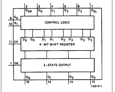
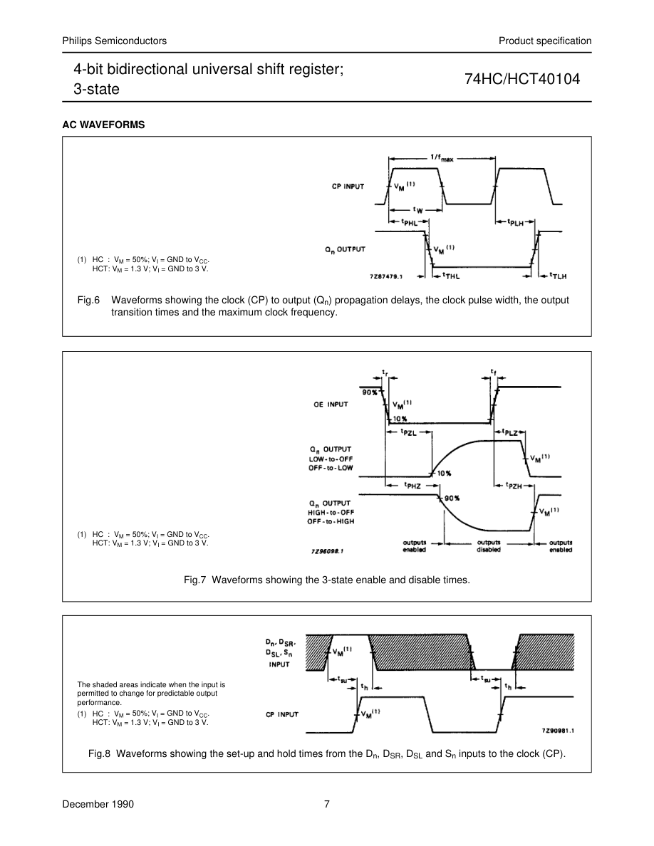
In the parallel-load mode (S0 and S1 are HIGH), data is loaded into the associated flip-flop and appears at the output after the positive transition of the clock input (CP). During loading, serial data flow is inhibited. Shift-right and shift-left are accomplished synchronously on the positive clock edge with serial data entered at the shift-right (DSR) and shift-left (DSL) serial inputs, respectively. Clearing the register is accomplished by setting both mode controls (S0 and S1) LOW and clocking the register. When the output enable input (OE) is LOW, all outputs assume the high-impedance OFF-state (Z).
APPLICATIONS
- Arithmetic unit bus registers
- Serial/parallel conversion
- General-purpose register for bus organized systems
- General-purpose registers
| SYMBOL | PARAMETER | CONDITIONS | TYPICAL | UNIT | |
|---|---|---|---|---|---|
| HC | HCT | ||||
| t / t PHL PLH | propagation delay CP to Q n | C = 15 pF; V = 5 V L CC | 13 | 15 | ns |
| f max | maximum clock frequency | 62 | 57 | MHz | |
| C I | input capacitance | 3.5 | 3.5 | pF | |
| C PD | power dissipation capacitance per package | notes 1 and 2 | 75 | 75 | pF |
Notes 1. CPD is used to determine the dynamic power dissipation (PD in µW): PD = CPD × VCC2 × fi + ∑ (CL × VCC2 × fo) where: fi = input frequency in MHz fo = output frequency in MHz ∑ (CL × VCC2 × fo) = sum of outputs CL = output load capacitance in pF VCC = supply voltage in V 2. For HC the condition is VI = GND to VCC For HCT the condition is VI = GND to VCC − 1.5 V
ORDERING INFORMATION
See “74HC/HCT/HCU/HCMOS Logic Package Information”.
Page 3
PIN DESCRIPTION
| PIN NO. | SYMBOL | NAME AND FUNCTION |
|---|---|---|
| 1 2 3, 4, 5, 6 7 8 9, 10 11 15, 14, 13, 12 16 | OE D SR D to D 0 3 D SL GND S , S 0 1 CP Q to Q 0 3 V CC | 3-state output enable input (active HIGH) serial data shift-right input parallel data inputs serial data shift-left input ground (0 V) mode control inputs clock input (LOW-to-HIGH, edge-triggered) 3-state parallel outputs positive supply voltage |
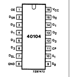
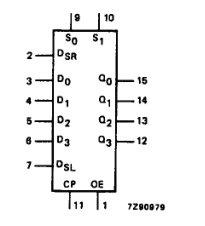
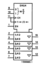
Fig.2 Logic symbol.
Fig.1 Pin configuration.
Fig.3 IEC logic symbol.
Page 4
FUNCTION TABLE
| Column 1 | Column 2 | Column 3 | Column 4 | Column 5 | Column 6 | Column 7 | Column 8 | Column 9 | Column 10 |
|---|---|---|---|---|---|---|---|---|---|
| OPE- RATING MODES | INPUTS (OE = HIGH) | OUTPUTS at t n+1 | |||||||
| S 1 | S 0 | D SR | D SL | D 0 to D 3 | Q 0 | Q 1 | Q 2 | Q 3 | |
| reset | L | L | X | X | X | L | L | L | L |
| shift left | H H | L L | X X | L H | X X | Q 1 Q 1 | Q 2 Q 2 | Q 3 Q 3 | L H |
| shift right | L L | H H | L H | X X | X X | L H | Q 0 Q 0 | Q 1 Q 1 | Q 2 Q 2 |
| parallel load | H H | H H | X X | X X | L H | L H | L H | L H | L H |
Notes 1. H = HIGH voltage level L = LOW voltage level X = don’t care tn+1 = state after next LOW-to-HIGH transition of CP
Fig.4 Functional diagram.
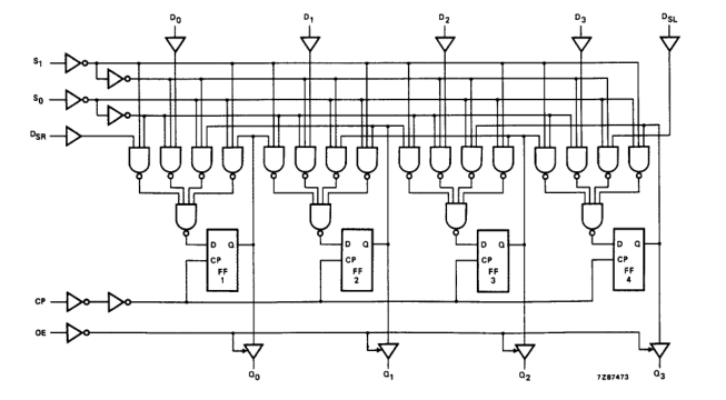
Fig.5 Logic diagram.
Page 5
DC CHARACTERISTICS FOR 74HC
For the DC characteristics see “74HC/HCT/HCU/HCMOS Logic Family Specifications”. Output capability: bus driver ICC category: MSI
AC CHARACTERISTICS FOR 74HC
GND = 0 V; tr = tf = 6 ns; CL = 50 pF
| SYMBOL | PARAMETER | T (°C) amb | UNIT | TEST CONDITIONS | |||||||
|---|---|---|---|---|---|---|---|---|---|---|---|
| 74HC | V CC (V) | WAVEFORMS | |||||||||
| +25 | −40 to +85 | −40 to +125 | |||||||||
| min. | typ. | max. | min. | max. | min. | max. | |||||
| t / t PHL PLH | propagation delay CP to Q n | 44 16 13 | 170 34 29 | 215 43 37 | 255 51 43 | ns | 2.0 4.5 6.0 | Fig.6 | |||
| t / t PZH PZL | 3-state output enable time OE to Q n | 33 12 10 | 150 30 26 | 190 38 33 | 225 45 38 | ns | 2.0 4.5 6.0 | Fig.8 | |||
| t / t PHZ PLZ | 3-state output disable time OE to Q n | 50 18 14 | 150 30 26 | 190 38 33 | 225 45 38 | ns | 2.0 4.5 6.0 | Fig.8 | |||
| t / t THL TLH | output transition time | 14 5 4 | 60 12 10 | 75 15 13 | 90 18 15 | ns | 2.0 4.5 6.0 | Fig.6 | |||
| t W | clock pulse width HIGH or LOW | 80 16 14 | 11 4 3 | 100 20 17 | 120 24 20 | ns | 2.0 4.5 6.0 | Fig.6 | |||
| t su | set-up time D n, D SR, D to CP SL | 80 16 14 | 17 6 5 | 100 20 17 | 120 24 20 | ns | 2.0 4.5 6.0 | Fig.8 | |||
| t su | set-up time S 0, S to CP 1 | 80 16 14 | 22 8 6 | 100 20 17 | 120 24 20 | ns | 2.0 4.5 6.0 | Fig.8 | |||
| t h | hold time D n, D SR, D to CP SL | 2 2 2 | −8 −3 −2 | 2 2 2 | 2 2 2 | ns | 2.0 4.5 6.0 | Fig.8 | |||
| t h | hold time S 0, S to CP 1 | 2 2 2 | −14 −5 −4 | 2 2 2 | 2 2 2 | ns | 2.0 4.5 6.0 | Fig.8 | |||
| f max | maximum clock pulse frequency | 6.0 30 35 | 19 56 67 | 4.8 24 28 | 4.0 20 24 | MHz | 2.0 4.5 6.0 | Fig.6 |
Page 6
DC CHARACTERISTICS FOR 74HCT
For the DC characteristics see “74HC/HCT/HCU/HCMOS Logic Family Specifications”. Output capability: bus driver ICC category: MSI
Note to HCT types The value of additional quiescent supply current (∆ICC) for a unit load of 1 is given in the family specifications. To determine ∆ICC per input, multiply this value by the unit load coefficient shown in the table below.
| INPUT | UNIT LOAD COEFFICIENT |
|---|---|
| D to D 0 3 D , D SR SL CP S , S 0 1 OE | 0.35 0.35 0.35 0.70 1.40 |
AC CHARACTERISTICS FOR 74HCT
GND = 0 V; tr = tf = 6 ns; CL = 50 pF
| SYMBOL | PARAMETER | T (°C) amb | UNIT | TEST CONDITIONS | |||||||
|---|---|---|---|---|---|---|---|---|---|---|---|
| 74HCT | V CC (V) | WAVEFORMS | |||||||||
| +25 | −40 to +85 | −40 to +125 | |||||||||
| min. | typ. | max. | min. | max. | min. | max. | |||||
| t / t PHL PLH | propagation delay CP to Q n | 18 | 34 | 43 | 51 | ns | 4.5 | Fig.6 | |||
| t / t PZH PZL | 3-state output enable time OE to Q n | 12 | 30 | 38 | 45 | ns | 4.5 | Fig.8 | |||
| t / t PHZ PLZ | 3-state output disable time OE to Q n | 21 | 35 | 44 | 53 | ns | 4.5 | Fig.8 | |||
| t / t THL TLH | output transition time | 5 | 12 | 15 | 18 | ns | 4.5 | Fig.6 | |||
| t W | clock pulse width HIGH or LOW | 16 | 7 | 20 | 24 | ns | 4.5 | Fig.6 | |||
| t su | set-up time D n, D SR, D to CP SL | 16 | 8 | 20 | 24 | ns | 4.5 | Fig.8 | |||
| t su | set-up time S 0, S to CP 1 | 20 | 9 | 25 | 30 | ns | 4.5 | Fig.8 | |||
| t h | hold time D n, D SR, D to CP SL | 2 | −2 | 2 | 2 | ns | 4.5 | Fig.8 | |||
| t h | hold time S 0, S to CP 1 | 2 | −5 | 2 | 2 | ns | 4.5 | Fig.8 | |||
| f max | maximum clock pulse frequency | 27 | 52 | 22 | 18 | MHz | 4.5 | Fig.6 |
Page 7
Page 8