

74HC3G34 NXP
Document overview
- PDF pages: 13
Technical content
Page 1
1. General description
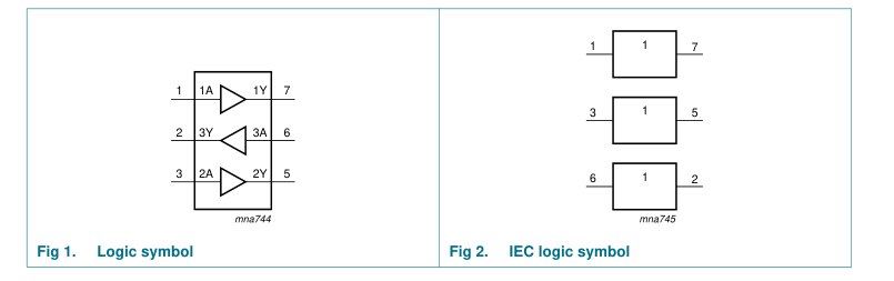
The 74HC3G34; 74HCT3G34 are high-speed Si-gate CMOS devices. They provide three buffer gates.
The HC device has CMOS input switching levels and supply voltage range 2 V to 6 V.
The HCT device has TTL input switching levels and supply voltage range 4.5 V to 5.5 V.
2. Features
I Wide supply voltage range from 2.0 V to 6.0 V I Symmetrical output impedance I High noise immunity I Low-power dissipation I Balanced propagation delays I Multiple package options I ESD protection: N HBM JESD22-A114E exceeds 2000 V N MM JESD22-A115-A exceeds 200 V I Specified from −40 °C to +85 °C and −40 °C to +125 °C
3. Ordering information
Table 1. Ordering information
| Type number | Package | |||
|---|---|---|---|---|
| Temperature range | Name | Description | Version |
−40 °C to +125 °C TSSOP8 plastic thin shrink small outline package; 8 leads;
74HC3G34DP
SOT505-2
body width 3 mm; lead length 0.5 mm
74HCT3G34DP
−40 °C to +125 °C VSSOP8 plastic very thin shrink small outline package; 8 leads;
74HC3G34DC
SOT765-1
body width 2.3 mm
74HCT3G34DC
−40 °C to +125 °C XSON8U plastic extremely thin small outline package; no leads;
74HC3G34GD
SOT996-2
8 terminals; UTLP based; body 3 × 2 × 0.5 mm
74HCT3G34GD

Page 2
4. Marking
Table 2. Marking Type number
Marking code
74HC3G34DP
H34
74HCT3G34DP
T34
74HC3G34DC
P34
74HCT3G34DC
U34
74HC3G34GD
P34
74HCT3G34GD
U34
5. Functional diagram
6. Pinning information
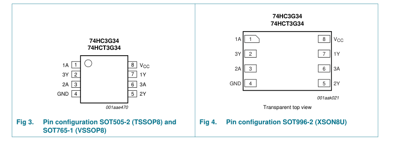
6.1 Pinning
2 of 13
Page 3
6.2 Pin description
Table 3. Pin description Symbol
Pin
Description
1A, 2A, 3A
1, 3, 6
data input
1Y, 2Y, 3Y
7, 5, 2
data output
GND
4
ground (0 V)
8
supply voltage
VCC
7. Functional description
Table 4. Function table [1]
| Column 1 | Column 2 |
|---|---|
| Input | Output |
| nA | nY |
L
L
H
H
[1] H = HIGH voltage level; L = LOW voltage level.
8. Limiting values
Table 5. Limiting values In accordance with the Absolute Maximum Rating System (IEC 60134). Voltages are referenced to GND (ground = 0 V). Symbol Parameter
Conditions
Min Max Unit
supply voltage
−0.5 +7.0 V
VCC
[1] -
input clamping current
VI < −0.5 V or VI > VCC + 0.5 V
±20 mA
IIK
[1] -
output clamping current
VO < −0.5 V or VO > VCC + 0.5 V
±20 mA
IOK
output current
VO = −0.5 V to (VCC + 0.5 V)
- ±25 mA
IO
quiescent supply current
- 50 mA
ICC
ground current
−50 - mA
IGND
storage temperature
−65 +150 °C
Tstg
[2] -
total power dissipation
Tamb = −40 °C to +125 °C
300 mW
Ptot
[1] The input and output voltage ratings may be exceeded if the input and output current ratings are observed. [2] For TSSOP8 package: above 55 °C the value of Ptot derates linearly with 2.5 mW/K. For VSSOP8 package: above 110 °C the value of Ptot derates linearly with 8 mW/K. For XSON8U package: above 118 °C the value of Ptot derates linearly with 7.8 mW/K.
3 of 13
Page 4
9. Recommended operating conditions
Table 6. Recommended operating conditions Voltages are referenced to GND (ground = 0 V).
| Symbol | Parameter | Conditions | 74HC3G34 | 74HCT3G34 | Unit | ||||
|---|---|---|---|---|---|---|---|---|---|
| Min | Typ | Max | Min | Typ | Max |
supply voltage
2.0 5.0 6.0 4.5 5.0 5.5 V
VCC input voltage
0 - VCC 0 - VCC V
VI output voltage
0 - VCC 0 - VCC V
VO ambient temperature
−40 +25 +125 −40 +25 +125 °C
Tamb
VCC = 2.0 V
- - 625 - - - ns/V
∆t/∆V input transition rise and fall rate
VCC = 4.5 V
- 1.67 139 - 1.67 139 ns/V
VCC = 6.0 V
- - 83 - - - ns/V
10. Static characteristics
Table 7. Static characteristics Voltages are referenced to GND (ground = 0 V).
| Symbol | Parameter | Conditions | −40 °C to +85 °C | −40 °C to +125 °C | Unit | |||
|---|---|---|---|---|---|---|---|---|
| Min | Typ[1] | Max | Min | Max |
74HC3G34 HIGH-level input
VCC = 2.0 V
1.5 1.2 - 1.5
- V
VIH voltage
VCC = 4.5 V
3.15 2.4
- 3.15
- V
VCC = 6.0 V
4.2 3.2 - 4.2
- V
LOW-level input
VCC = 2.0 V
- 0.8 0.5 - 0.5 V
VIL voltage
VCC = 4.5 V
- 2.1 1.35
- 1.35 V
VCC = 6.0 V
- 2.8 1.8 - 1.8 V
HIGH-level output
VI = VIH or VIL
VOH voltage
IO = −20 µA; VCC = 2.0 V
1.9 2.0 - 1.9
- V
IO = −20 µA; VCC = 4.5 V
4.4 4.5 - 4.4
- V
IO = −20 µA; VCC = 6.0 V
5.9 6.0 - 5.9
- V
IO = −4.0 mA; VCC = 4.5 V
4.13 4.32
- 3.7
- V
IO = −5.2 mA; VCC = 6.0 V
5.63 5.81
- 5.2
- V
LOW-level output
VI = VIH or VIL
VOL voltage
IO = 20 µA; VCC = 2.0 V
- 0 0.1 - 0.1 V
IO = 20 µA; VCC = 4.5 V
- 0 0.1 - 0.1 V
IO = 20 µA; VCC = 6.0 V
- 0 0.1 - 0.1 V
IO = 4.0 mA; VCC = 4.5 V
- 0.15 0.33
- 0.4 V
IO = 5.2 mA; VCC = 6.0 V
- 0.16 0.33
- 0.4 V
input leakage current
VI = VCC or GND; VCC = 6.0 V
- - ±1.0 - ±1.0 µA
II supply current
per input pin; VI = VCC or GND;
- - 10 - 20 µA
ICC
IO = 0 A; VCC = 6.0 V
input capacitance
- 1.5 - - - pF
CI
4 of 13
Page 5
Table 7. Static characteristics …continued Voltages are referenced to GND (ground = 0 V).
| Symbol | Parameter | Conditions | −40 °C to +85 °C | −40 °C to +125 °C | Unit | |||
|---|---|---|---|---|---|---|---|---|
| Min | Typ[1] | Max | Min | Max |
74HCT3G34
HIGH-level input
VCC = 4.5 V to 5.5 V
2.0 1.6 - 2.0
- V
VIH voltage LOW-level input
VCC = 4.5 V to 5.5 V
- 1.2 0.8 - 0.8 V
VIL voltage HIGH-level output
VI = VIH or VIL
VOH voltage
IO = −20 µA; VCC = 4.5 V
4.4 4.5 - 4.4
- V
IO = −4.0 mA; VCC = 4.5 V
4.13 4.32
- 3.7
- V
LOW-level output
VI = VIH or VIL
VOL voltage
IO = 20 µA; VCC = 4.5 V
- 0 0.1 - 0.1 V
IO = 4.0 mA; VCC = 4.5 V
- 0.15 0.33
- 0.4 V
input leakage current
VI = VCC or GND; VCC = 5.5 V
- - ±1.0 - ±1.0 µA
II supply current
VI = VCC or GND; IO = 0 A;
- - 10 - 20 µA
ICC
VCC = 5.5 V
additional supply
per input; VCC = 4.5 V to 5.5 V;
- - 375 - 410 µA
∆ICC current
VI = VCC − 2.1 V; IO = 0 A
input capacitance
- 1.5 - - - pF
CI
[1] All typical values are measured at Tamb = 25 °C.
11. Dynamic characteristics
Table 8. Dynamic characteristics Voltages are referenced to GND (ground = 0 V); for test circuit see Figure 6.
| Symbol | Parameter | Conditions | −40 °C to +85 °C | −40 °C to +125 °C | Unit | |||
|---|---|---|---|---|---|---|---|---|
| Min | Typ[1] | Max | Min | Max |
74HC3G34
[2]
propagation delay nA to nY; see Figure 5 tpd
VCC = 2.0 V
- 29 95 - 125 ns
VCC = 4.5 V
- 9 19 - 25 ns
VCC = 6.0 V
- 8 16 - 20 ns
[3]
transition time
nY; see Figure 5
tt
VCC = 2.0 V
- 18 95 - 125 ns
VCC = 4.5 V
- 6 19 - 25 ns
VCC = 6.0 V
- 5 16 - 20 ns
[4]
power dissipation
VI = GND to VCC
- 10 - - - pF
CPD capacitance
5 of 13
Page 6
Table 8. Dynamic characteristics …continued Voltages are referenced to GND (ground = 0 V); for test circuit see Figure 6.
| Symbol | Parameter | Conditions | −40 °C to +85 °C | −40 °C to +125 °C | Unit | |||
|---|---|---|---|---|---|---|---|---|
| Min | Typ[1] | Max | Min | Max |
74HCT3G34
[2]
propagation delay nA to nY; see Figure 5 tpd
VCC = 4.5 V
- 10 23 - 29 ns
[3]
transition time
nY; VCC = 4.5 V; see Figure 5
- 6 19 - 25 ns
tt
[4]
power dissipation
VI = GND to VCC − 1.5 V
- 9 - - - pF
CPD capacitance
[1] All typical values are measured at Tamb = 25 °C. [2] tpd is the same as tPLH and tPHL. [3] tt is the same as tTLH and tTHL. [4] CPD is used to determine the dynamic power dissipation (PD in µW). PD = CPD × VCC2 × fi × N + Σ(CL × VCC2 × fo) where: fi = input frequency in MHz; fo = output frequency in MHz; CL = output load capacitance in pF; VCC = supply voltage in V; N = number of inputs switching; Σ(CL × VCC2 × fo) = sum of outputs.
12. Waveforms
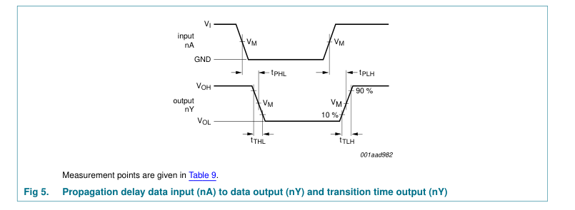
Table 9. Measurement points
| Type | Input | Output |
|---|---|---|
| V M | V M |
74HC3G34
0.5 × VCC
0.5 × VCC
74HCT3G34
1.3 V
1.3 V
6 of 13
Page 7
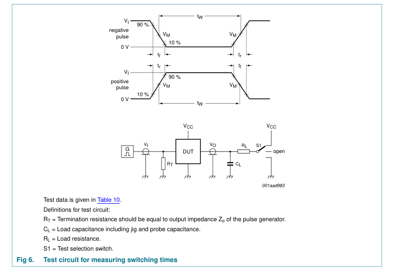
Table 10. Test data
| Type | Input | Load | S1 position | ||
|---|---|---|---|---|---|
| V I | t, t r f | C L | R L | t , t PHL PLH |
74HC3G34
GND to VCC
≤ 6 ns
50 pF
1 kΩ
open
74HCT3G34
GND to 3 V
≤ 6 ns
50 pF
1 kΩ
open
7 of 13
Page 8
13. Package outline
TSSOP8: plastic thin shrink small outline package; 8 leads; body width 3 mm; lead length 0.5 mm
SOT505-2
D
E
A X
c
HE
v M A
y
Z
5
8
A2 A
(A3)
A1
pin 1 index
θ Lp L
1
4
detail X
w M
e bp
0
2.5
5 mm
scale
DIMENSIONS (mm are the original dimensions)
| UNIT | A max. | A1 | A2 | A3 | bp | c | D(1) | E(1) | e | HE | L | Lp | v | w | y | Z(1) | θ |
|---|---|---|---|---|---|---|---|---|---|---|---|---|---|---|---|---|---|
| mm | 1.1 | 0.15 0.00 | 0.95 0.75 | 0.25 | 0.38 0 0.22 0 | .18 .08 | 3.1 2.9 | 3.1 2.9 | 0.65 | 4.1 3.9 | 0.5 | 0.47 0.33 | 0.2 | 0.13 | 0.1 | 0.70 0.35 | 8° 0° |
Note 1. Plastic or metal protrusions of 0.15 mm maximum per side are not included.
REFERENCES
OUTLINE
EUROPEAN
ISSUE DATE
VERSION
PROJECTION
IEC
JEDEC
JEITA
02-01-16
SOT505-2
- - -
Fig 7. Package outline SOT505-2 (TSSOP8)
8 of 13
Page 9
VSSOP8: plastic very thin shrink small outline package; 8 leads; body width 2.3 mm
SOT765-1
D
E
A X
c
y
HE
v M A
Z
5
8
Q
A2 A A1
(A3)
pin 1 index
θ Lp L
1
4
detail X
e
w M bp
0
2.5
5 mm
scale
DIMENSIONS (mm are the original dimensions)
| UNIT | A max. | A1 | A2 | A3 | bp | c | D(1) | E(2) | e | HE | L | Lp | Q | v | w | y | Z(1) | θ |
|---|---|---|---|---|---|---|---|---|---|---|---|---|---|---|---|---|---|---|
| mm | 1 | 0.15 0.00 | 0.85 0.60 | 0.12 | 0.27 0.17 | 0.23 0.08 | 2.1 1.9 | 2.4 2.2 | 0.5 | 3.2 3.0 | 0.4 | 0.40 0.15 | 0.21 0.19 | 0.2 | 0.13 | 0.1 | 0.4 0.1 | 8° 0° |
Notes 1. Plastic or metal protrusions of 0.15 mm maximum per side are not included. 2. Plastic or metal protrusions of 0.25 mm maximum per side are not included.
REFERENCES
OUTLINE
EUROPEAN
ISSUE DATE
VERSION
PROJECTION
IEC
JEDEC
JEITA
02-06-07
SOT765-1
MO-187
Fig 8. Package outline SOT765-1 (VSSOP8)
9 of 13
Page 10
XSON8U: plastic extremely thin small outline package; no leads;
SOT996-2
8 terminals; UTLP based; body 3 x 2 x 0.5 mm
B A
D
A
E
A1
detail X
terminal 1 index area
e1
C
C A B v M b e
L1
y
y1 C
w M C
1
4
L2
L
8
5
X
0 1 2 mm scale
DIMENSIONS (mm are the original dimensions)
| UNIT | A max | A1 | b | D | E | e | e1 | L | L1 | L2 | v | w | y | y1 |
|---|---|---|---|---|---|---|---|---|---|---|---|---|---|---|
| mm | 0.5 | 0.05 0.00 | 0.35 0.15 | 2.1 1.9 | 3.1 2.9 | 0.5 | 1.5 | 0.5 0.3 | 0.15 0.05 | 0.6 0.4 | 0.1 | 0.05 | 0.05 | 0.1 |
| Column 1 | Column 2 | Column 3 | Column 4 | Column 5 | Column 6 | Column 7 |
|---|---|---|---|---|---|---|
| OUTLINE VERSION | REFERENCES IEC JEDEC JEITA | EUROPEAN PROJECTION | ISSUE DATE | |||
| IEC | JEDEC | JEITA | ||||
| SOT996-2 | - - - | - - - | 07-12-18 07-12-21 |
Fig 9. Package outline SOT996-2 (XSON8U)
10 of 13
Page 11
14. Abbreviations
Table 11. Abbreviations Acronym
Description
CMOS
Complementary Metal Oxide Semiconductor
DUT
Device Under Test
ESD
ElectroStatic Discharge
HBM
Human Body Model
MM
Machine Model
TTL
Transistor-Transistor Logic
15. Revision history
Table 12. Revision history Document ID
Release date
Data sheet status
Change notice
Supersedes
20090507
-
74HC_HCT3G34_4
- The format of this data sheet has been redesigned to comply with the new identity
Modifications:
guidelines of NXP Semiconductors.
- Legal texts have been adapted to the new company name where appropriate.
- Added type number 74HC3G34GD and 74HCT3G34GD (XSON8U package)
74HC_HCT3G34_4
20060309
-
74HC_HCT3G34_3
20030519
Product specification
-
74HC_HCT3G34_2
20030210
Product specification
-
74HC_HCT3G34_1
20031003
Product specification
-
74HC_HCT3G34_3 74HC_HCT3G34_2 74HC_HCT3G34_1 -
11 of 13
Page 12
16. Legal information
16.1 Data sheet status
Document status[1][2]
Product status[3]
Definition This document contains data from the objective specification for product development.
Objective [short] data sheet
Development
This document contains data from the preliminary specification.
Preliminary [short] data sheet Qualification
This document contains the product specification.
Product [short] data sheet
Production
[1] Please consult the most recently issued document before initiating or completing a design. [2] The term ‘short data sheet’ is explained in section “Definitions”. [3] The product status of device(s) described in this document may have changed since this document was published and may differ in case of multiple devices. The latest product status information is available on the Internet at URL http://www.nxp.com.
16.2 Definitions
Draft — The document is a draft version only. The content is still under internal review and subject to formal approval, which may result in modifications or additions. NXP Semiconductors does not give any representations or warranties as to the accuracy or completeness of information included herein and shall have no liability for the consequences of use of such information. Short data sheet — A short data sheet is an extract from a full data sheet with the same product type number(s) and title. A short data sheet is intended for quick reference only and should not be relied upon to contain detailed and full information. For detailed and full information see the relevant full data
sheet, which is available on request via the local NXP Semiconductors sales office. In case of any inconsistency or conflict with the short data sheet, the full data sheet shall prevail.
16.3 Disclaimers
General — Information in this document is believed to be accurate and reliable. However, NXP Semiconductors does not give any representations or warranties, expressed or implied, as to the accuracy or completeness of such information and shall have no liability for the consequences of use of such information. Right to make changes — NXP Semiconductors reserves the right to make changes to information published in this document, including without limitation specifications and product descriptions, at any time and without notice. This document supersedes and replaces all information supplied prior to the publication hereof. Suitability for use — NXP Semiconductors products are not designed,
authorized or warranted to be suitable for use in medical, military, aircraft, space or life support equipment, nor in applications where failure or malfunction of an NXP Semiconductors product can reasonably be expected to result in personal injury, death or severe property or environmental
17. Contact information
For more information, please visit: http://www.nxp.com
damage. NXP Semiconductors accepts no liability for inclusion and/or use of NXP Semiconductors products in such equipment or applications and therefore such inclusion and/or use is at the customer’s own risk. Applications — Applications that are described herein for any of these products are for illustrative purposes only. NXP Semiconductors makes no representation or warranty that such applications will be suitable for the specified use without further testing or modification. Limiting values — Stress above one or more limiting values (as defined in the Absolute Maximum Ratings System of IEC 60134) may cause permanent damage to the device. Limiting values are stress ratings only and operation of
the device at these or any other conditions above those given in the Characteristics sections of this document is not implied. Exposure to limiting values for extended periods may affect device reliability. Terms and conditions of sale — NXP Semiconductors products are sold subject to the general terms and conditions of commercial sale, as published at http://www.nxp.com/profile/terms, including those pertaining to warranty, intellectual property rights infringement and limitation of liability, unless explicitly otherwise agreed to in writing by NXP Semiconductors. In case of any inconsistency or conflict between information in this document and such terms and conditions, the latter will prevail.
No offer to sell or license — Nothing in this document may be interpreted or construed as an offer to sell products that is open for acceptance or the grant, conveyance or implication of any license under any copyrights, patents or other industrial or intellectual property rights. Export control — This document as well as the item(s) described herein may be subject to export control regulations. Export might require a prior authorization from national authorities.
16.4 Trademarks
Notice: All referenced brands, product names, service names and trademarks are the property of their respective owners.
For sales office addresses, please send an email to: salesaddresses@nxp.com
12 of 13
Page 13
18. Contents
1 General description . . . . . . . . . . . . . . . . . . . . . . 1 2 Features . . . . . . . . . . . . . . . . . . . . . . . . . . . . . . . 1 3 Ordering information . . . . . . . . . . . . . . . . . . . . . 1 4 Marking . . . . . . . . . . . . . . . . . . . . . . . . . . . . . . . . 2 5 Functional diagram . . . . . . . . . . . . . . . . . . . . . . 2 6 Pinning information. . . . . . . . . . . . . . . . . . . . . . 2 6.1 Pinning . . . . . . . . . . . . . . . . . . . . . . . . . . . . . . . 2 6.2 Pin description . . . . . . . . . . . . . . . . . . . . . . . . . 3 7 Functional description . . . . . . . . . . . . . . . . . . . 3 8 Limiting values. . . . . . . . . . . . . . . . . . . . . . . . . . 3
9 Recommended operating conditions. . . . . . . . 4 10 Static characteristics. . . . . . . . . . . . . . . . . . . . . 4 11 Dynamic characteristics . . . . . . . . . . . . . . . . . . 5 12 Waveforms . . . . . . . . . . . . . . . . . . . . . . . . . . . . . 6 13 Package outline . . . . . . . . . . . . . . . . . . . . . . . . . 8 14 Abbreviations. . . . . . . . . . . . . . . . . . . . . . . . . . 11 15 Revision history. . . . . . . . . . . . . . . . . . . . . . . . 11 16 Legal information. . . . . . . . . . . . . . . . . . . . . . . 12 16.1 Data sheet status . . . . . . . . . . . . . . . . . . . . . . 12 16.2 Definitions. . . . . . . . . . . . . . . . . . . . . . . . . . . . 12
16.3 Disclaimers . . . . . . . . . . . . . . . . . . . . . . . . . . . 12 16.4 Trademarks. . . . . . . . . . . . . . . . . . . . . . . . . . . 12 17 Contact information. . . . . . . . . . . . . . . . . . . . . 12 18 Contents . . . . . . . . . . . . . . . . . . . . . . . . . . . . . . 13

Please be aware that important notices concerning this document and the product(s) described herein, have been included in section ‘Legal information’.
© NXP B.V. 2009.
All rights reserved.
For more information, please visit: http://www.nxp.com For sales office addresses, please send an email to: salesaddresses@nxp.com
Date of release: 7 May 2009 Document identifier: 74HC_HCT3G34_5