


 Download PDF
74HCT32 ONSEMI
Document overview
- PDF pages: 8
Technical content
Page 1
Quad 2−Input OR Gate with LSTTL−Compatible Inputs
High−Performance Silicon−Gate CMOS
The 74HCT32 is identical in pinout to the LS32. The device has TTL−compatible inputs.
Features
- Output Drive Capability: 10 LSTTL Loads
- TTL/NMOS−Compatible Input Levels
- Outputs Directly Interface to CMOS, NMOS and TTL
- Operating Voltage Range: 4.5 to 5.5 V
- Low Input Current: 1.0 ?A
- High Noise Immunity Characteristic of CMOS Devices
- In Compliance With the JEDEC Standard No. 7A Requirements
- ESD Performance: HBM ? 2000 V; Machine Model ? 200 V
- Chip Complexity: 48 FETs or 12 Equivalent Gates
- These are Pb−Free Devices
© Semiconductor Components Industries, LLC, 2007 March, 2007 − Rev. 0

MARKING DIAGRAMS
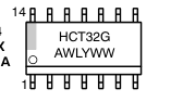
SOIC−14
14
D SUFFIX
CASE 751A
1
14 HCT
TSSOP−14
14
32
DT SUFFIX
ALYW?
CASE 948G
1
? 1
HCT32 = Device Code A = Assembly Location L, WL = Wafer Lot Y = Year W, WW = Work Week G or ? = Pb−Free Package (Note: Microdot may be in either location)
ORDERING INFORMATION
See detailed ordering and shipping information in the package dimensions section on page 2 of this data sheet.
Publication Order Number:
74HCT32/D
Page 2
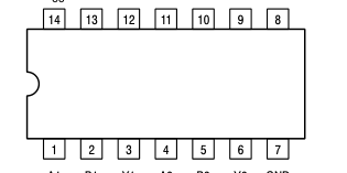
Pinout: 14−Lead Packages (Top View)
LOGIC DIAGRAM
1
B4 A4 Y4 B3 A3 Y3 VCC
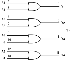
Y = A+B
A1 B1 Y1 A2 B2 Y2 GND
FUNCTION TABLE
PIN 14 = VCC
| Column 1 | Column 2 | Column 3 |
|---|---|---|
| Inputs | Output | |
| A | B | Y |
| L L H H | L H L H | L H H H |
PIN 7 = GND
ORDERING INFORMATION
| Column 1 | Column 2 | Column 3 |
|---|---|---|
| Device | Package | Shipping† |
| 74HCT32DR2G | SOIC−14 (Pb−Free) | 2500 / Tape & Reel |
| 74HCT32DTR2G | TSSOP−14* |
†For information on tape and reel specifications, including part orientation and tape sizes, please refer to our Tape and Reel Packaging Specifications Brochure, BRD8011/D. \*This package is inherently Pb−Free.
Page 3
MAXIMUM RATINGS
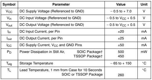
Stresses exceeding Maximum Ratings may damage the device. Maximum Ratings are stress ratings only. Functional operation above the Recommended Operating Conditions is not implied. Extended exposure to stresses above the Recommended Operating Conditions may affect device reliability. †Derating — SOIC Package: – 7 mW/?C from 65? to 125?C
TSSOP Package: − 6.1 mW/?C from 65? to 125?C
For high frequency or heavy load considerations, see Chapter 2 of the ON Semiconductor High−Speed CMOS Data Book (DL129/D).
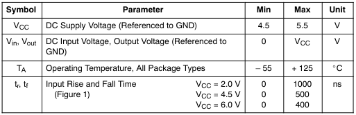
RECOMMENDED OPERATING CONDITIONS
Page 4
DC CHARACTERISTICS (Voltages Referenced to GND)
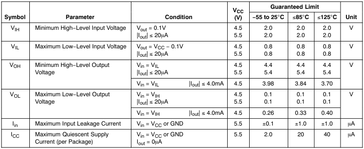

- Information on typical parametric values can be found in Chapter 2 of the ON Semiconductor High−Speed CMOS Data Book (DL129/D). 2. Total Supply Current = ICC + Σ?ICC.
AC CHARACTERISTICS (CL = 50pF, Input tr = tf = 6ns)
| Symbol | Parameter | VCC (V) | Guaranteed Limit | Unit | ||
|---|---|---|---|---|---|---|
| −55 to 25°C | ≤85°C | ≤125°C | ||||
| tPLH, tPHL | Maximum Propagation Delay, Input A or B to Output Y (Figures 1 and 2) | 4.5 | 15 | 19 | 22 | ns |
| tTLH, tTHL | Maximum Output Transition Time, Any Output (Figures 1 and 2) | 4.5 | 15 | 19 | 22 | ns |
| Cin | Maximum Input Capacitance | 10 | 10 | 10 | pF |
NOTE: For propagation delays with loads other than 50 pF, and information on typical parametric values, see Chapter 2 of the ON Semiconductor High−Speed CMOS Data Book (DL129/D).
| CPD | Power Dissipation Capacitance (Per Buffer)* | Typical @ 25°C, VCC = 5.0 V, VEE = 0 V | pF |
|---|---|---|---|
| 20 |
\* Used to determine the no−load dynamic power consumption: PD = CPD VCC2f + ICC VCC. For load considerations, see Chapter 2 of the ON Semiconductor High−Speed CMOS Data Book (DL129/D).
Page 5
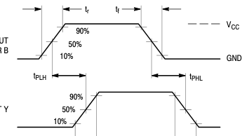
INPUT A OR B
OUTPUT Y
tTHL
tTLH
Figure 1. Switching Waveforms
TEST POINT
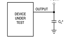
\*Includes all probe and jig capacitance
Figure 2. Test Circuit
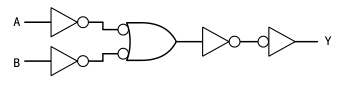
Figure 3. Expanded Logic Diagram (1/4 of the Device)
Page 6
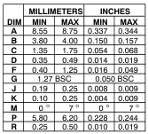
PACKAGE DIMENSIONS
SOIC−14
CASE 751A−03
ISSUE H
NOTES: 1. DIMENSIONING AND TOLERANCING PER
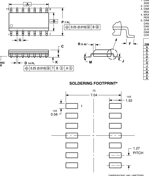
ANSI Y14.5M, 1982. 2. CONTROLLING DIMENSION: MILLIMETER. 3. DIMENSIONS A AND B DO NOT INCLUDE MOLD PROTRUSION. 4. MAXIMUM MOLD PROTRUSION 0.15 (0.006) PER SIDE. 5. DIMENSION D DOES NOT INCLUDE DAMBAR PROTRUSION. ALLOWABLE DAMBAR PROTRUSION SHALL BE 0.127 (0.005) TOTAL IN EXCESS OF THE D DIMENSION AT MAXIMUM MATERIAL CONDITION.
−T−
SEATING
PLANE
DIMENSIONS: MILLIMETERS
\*For additional information on our Pb−Free strategy and soldering
details, please download the ON Semiconductor Soldering and
Mounting Techniques Reference Manual, SOLDERRM/D.
Page 7
PACKAGE DIMENSIONS
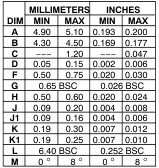
TSSOP−14
CASE 948G−01
ISSUE B
NOTES:
K
- DIMENSIONING AND TOLERANCING PER
14X REF
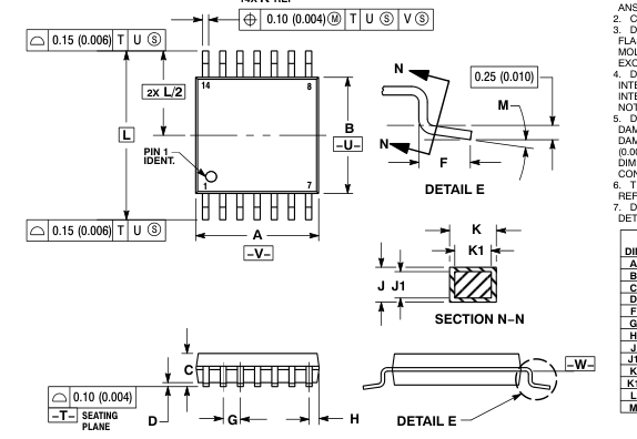
ANSI Y14.5M, 1982. CONTROLLING DIMENSION: MILLIMETER. DIMENSION A DOES NOT INCLUDE MOLD FLASH, PROTRUSIONS OR GATE BURRS. MOLD FLASH OR GATE BURRS SHALL NOT EXCEED 0.15 (0.006) PER SIDE. DIMENSION B DOES NOT INCLUDE INTERLEAD FLASH OR PROTRUSION. INTERLEAD FLASH OR PROTRUSION SHALL NOT EXCEED 0.25 (0.010) PER SIDE. DIMENSION K DOES NOT INCLUDE DAMBAR PROTRUSION. ALLOWABLE DAMBAR PROTRUSION SHALL BE 0.08 (0.003) TOTAL IN EXCESS OF THE K DIMENSION AT MAXIMUM MATERIAL CONDITION. TERMINAL NUMBERS ARE SHOWN FOR REFERENCE ONLY. DIMENSION A AND B ARE TO BE DETERMINED AT DATUM PLANE −W−.
SOLDERING FOOTPRINT\*
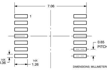
\*For additional information on our Pb−Free strategy and soldering
details, please download the ON Semiconductor Soldering and
Mounting Techniques Reference Manual, SOLDERRM/D.
Page 8

PUBLICATION ORDERING INFORMATION
N. American Technical Support: 800−282−9855 Toll Free
ON Semiconductor Website: www.onsemi.com
LITERATURE FULFILLMENT: Literature Distribution Center for ON Semiconductor
USA/Canada Europe, Middle East and Africa Technical Support:
Order Literature: http://www.onsemi.com/orderlit
P.O. Box 5163, Denver, Colorado 80217 USA Phone: 303−675−2175 or 800−344−3860 Toll Free USA/Canada Phone: 421 33 790 2910
For additional information, please contact your local
Fax: 303−675−2176 or 800−344−3867 Toll Free USA/Canada
Japan Customer Focus Center
Sales Representative
Email: orderlit@onsemi.com
Phone: 81−3−5773−3850