

 Download PDF
74HC164_1 ESTEK
Document overview
- Manufacturer or author: Provided By digicamel.com
- PDF pages: 6
Technical content
Features
- Outputs Directly Interface to CMOS, NMOS, and TTL
- Operating Voltage Range: 2.0 to 6.0 V
- Low Input Current: 1.0 µA
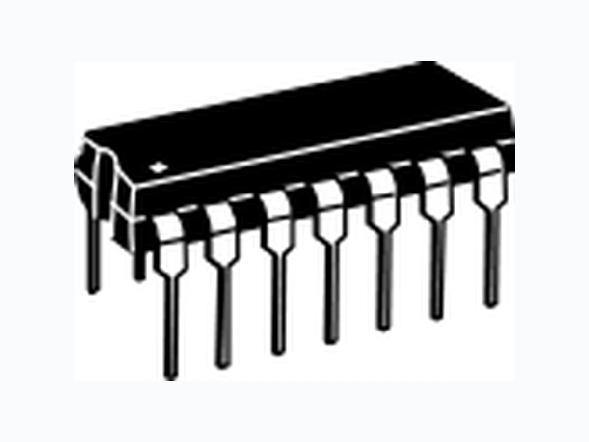
- High Noise Immunity Characteristic of CMOS Devices DIP - 14 Logic Diagram SOP –14 Package Pin Assignment Function Table Inputs Outputs RESET CLOCK A1 QA QB…QH L H H H X X X X X H D L L… L no change D QAn…QGn D D = data input X = don' t care QAn - QGn = data shifted from the previous stage on a rising edge at the clock input. BEIJING ESTEK ELECTRONICS CO.,LTD
Symbol Parameter Value Unit VCC DC Supply Voltage (Referenced to GND) -0.5 to +7.0 V VIN DC Input Voltage (Referenced to GND) -1.5 to VCC +1.5 V VOUT DC Output Voltage (Referenced to GND) -0.5 to VCC +0.5 V IIN DC Input Current, per Pin ±20 mA IOUT DC Output Current, per Pin ±25 mA ICC DC Supply Current, VCC and GND Pins ±50 mA PD Power Dissipation in Still Air, Plastic DIP+ 750 500 mW Tstg Storage Temperature -65 to +150 °C TL Lead Temperature, 1 mm from Case for 10 Seconds (Plastic DIP or SOIC Package) 260 °C *Maximum Ratings are those values beyond which damage to the device may occur. Functional operation should be restricted to the Recommended Operating Conditions. +Derating - Plastic DIP: - 10 mW/ °C from 65 °to 125°C Recommended Operating Conditions Symbol Parameter Min Max Unit VCC DC Supply Voltage (Referenced to GND) 2.0 6.0 V VIN, VOUT DC Input Voltage, Output Voltage (Referenced to GND) 0 VCC V TA Operating Temperature, All Package Types -55 +125 °C tr, tf Input Rise and Fall Time (Figure 1) VCC =2.0 V VCC =4.5 V VCC =6.0 1000 500 400 ns This device contains protection circuitry to guard against damage due to high static voltages or electric fields. However, precautions must betaken to avoid applications of any voltage higher than maximum rated voltages to this high-impedance circuit. For proper operation, VIN and VOUT should be constrained to the range GND≤(VIN or V OUT)≤VCC. Unused inputs must always be tied to an appropriate logic voltage level (e.g., either GND or VCC). BEIJING ESTEK ELECTRONICS CO.,LTD
(Voltages Referenced to GND) VCC Guaranteed Limit Symbol Parameter Test Conditions V 25 °C to -55°C 125 Unit VIH Minimum High- Level Input Voltage VIL Maximum Low - Level Input Voltage VOH Minimum High- Level Output Voltage VOL Maximum Low- Level Output Voltage VOUT=0.1 V or VCC-0.1 V IOUT≤ 20 µA VOUT=0.1 V or VCC-0.1 V IOUT ≤ 20 µA VIN= VIH or VIL IOUT ≤ 20 µA VIN= VIH or VIL IOUT ≤ 4.0 mA IOUT ≤ 5.2 mA VIN=VIH or VIL IOUT ≤ 20 µA VIN=VIH or VIL IOUT ≤ 4.0 mA I ≤ 5.2 mA 2.0 4.5 6.0 2.0 4.5 6.0 2.0 4.5 6.0 4.5 6.0 2.0 4.5 6.0 4.5 6.0 1.5 3.15 4.2 0.3 0.9 1.2 1.9 4.4 5.9 3.98 5.48 0.1 0.1 0.1 0.26 0.26 1.5 3.15 4.2 0.3 0.9 1.2 1.9 4.4 5.9 3.84 5.34 0.1 0.1 0.1 0.33 0.33 1.5 3.15 4.2 0.3 0.9 1.2 1.9 4.4 5.9 3.7 5.2 0.1 0.1 0.1 0.4 0.4 V V V V IIN Maximum Input Leakage Current VIN=VCC or GND 6.0 ±0.1 ±1.0 ±1.0 µA ICC Maximum Quiescent Supply Current VIN=VCC or GND IOUT=0µA 6.0 8.0 80 160 µA BEIJING ESTEK ELECTRONICS CO.,LTD
Symbol Parameter V 25 °C to -55°C ≤85°C ≤125°C Unit fmax Maximum Clock Frequency (50% Duty Cycle) (Figures 1 and 4) tPLH, tPHL Maximum Propagation Delay,Clock to Q (Figures 1 and 4) tPHL Maximum Propagation Delay,Reset to Q (Figures 2 and 4) tTLH, tTHL Maximum Output Transition Time, Any Output 2.0 4.5 6.0 2.0 4.5 6.0 2.0 4.5 6.0 2.0 4.5 6.0 6.0 175 205 4.8 220 255 4.0 265 310 110 MHz ns ns ns CIN Maximum Input Capacitance - 10 10 10 pF tSU Minimum Setup Time,A1 or A2 to Clock (Figure 3) th Minimum Hold Time, Clock to A1 or A2 (Figure 3) trec Minimum Recovery Time, Reset Inactive to Clock (Figure 2) 2.0 4.5 6.0 2.0 4.5 6.0 2.0 4.5 6.0 ns ns ns tw Minimum Pulse Width, Reset (Figure 2) 2.0 4.5 6.0 tw Minimum Pulse Width, Clock (Figure 1) 2.0 4.5 6.0 tr, tf Maximum Input Rise and Fall Times (Figure 1) 2.0 4.5 6.0 1000 500 400 100 100 1000 500 400 120 120 1000 500 400 ns ns ns Power Dissipation Capacitance (Per Package) CPD Used to determine the no-load dynamic power consumption: 2f+ICCVCCPD=CPDV Typical @25°C,VCC=5.0 V 140 pF BEIJING ESTEK ELECTRONICS CO.,LTD
Ordering Information
ORDERING NUMBER PACKAGE MARKING 74HC164 DIP - 14 / SOP - 14 ESTEK74HC164 Address : 6A06--6A07 Rm 6A07,Changyin Office Building ,No.88,Yong Ding Road,Hai Dian District ,Beijing Postalcode:100039 Tel: 86-010-58895780 / 81 / 82 / 83 / 84 Fax : 010-58895793 Http://www.estek.com.cn Email:sales@estek.com.cn REV No:01-060826 BEIJING ESTEK ELECTRONICS CO.,LTD