
74802 VISHAY
Document overview
- Manufacturer or author: Provided By www.digicamel.com(FREE DATASHEET DOWNLOAD SITE)
- PDF pages: 6
Technical content
Features
- Dropout Voltage 1.2V at 800mA Output Current
- Fast Transient Response
- Line Regulation typically at 0.015%
- Load Regulation typically at 0.1%
- Internal thermal limiting
- Adjustable Output Voltage or Fixed 2.5V, 2.85V, 3.3V, 5V
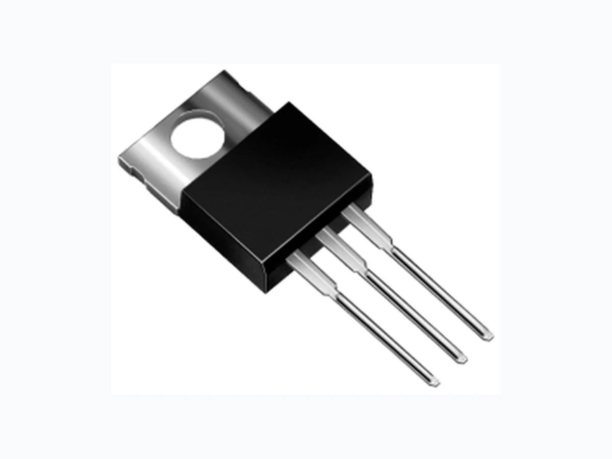
- Standard 3-Pin Power Packages TO-220AB TO-263AB (D2Pak) GS1117CT GS1117CMGS1117CE TO-252 (DPak) 2 3 2 3 GS1117CST SOT-223 Pin Definition 1.Adjust/Gnd. 2.Vout (tab) 3.Vin
formerly General Semiconductor www.vishay.com Document Number 74802 2 20-Feb-02 Maximum Ratings and Thermal Characteristics(TA = 25°C unless otherwise noted) Parameter Symbol Value Unit Vin Pin to ADJ/GND Pin Vin 7 V Thermal Resistance – Junction to Case TO-220AB 3.0 TO-252 R θJC 8.0 °C/W TO-263AB 3.0 SOT -223 15.0 Operating Junction Temperature Range T J 0 to +125 °C Storage Temperature Range T stg –65 to 150 °C Electrical Characteristics(1) TJ = 25°C (2), VIN = 5V, Io = 10mA unless otherwise noted. Parameter Symbol Test Conditions Min Typ Max Unit TJ = 25°C 1.238 1.250 1.262 V 0°C ≤ TJ ≤ 125°C 1.225 1.250 1.275 VReference Voltage V REF 2.65V ≤ VIN ≤ 7V 10mA ≤ Io ≤ 800mA GS1117-2.5, VIN = 5V 2.48 2.5 2.53 V GS1117-2.85, VIN = 5V 2.82 2.85 2.88 V GS1117-3.3, VIN = 5V 3.26 3.30 3.33 V Output Voltage V OUT GS1117-5, VIN = 7V 4.95 5.00 5.05 V GS1117 0.98V N VN 1.02VN V 0°C ≤ TJ ≤ 125°C 2.65V ≤ VIN ≤ 7V 10mA ≤ Io ≤ 800mA 2.65V ≤ VIN ≤ 7V Line Regulation REG line TJ = 25°C 0.015 0.2 % V O 0°C ≤ TJ ≤ 125°C 0.02 0.2 % V O 10mA ≤ Io ≤ 800mA Load Regulation REG load TJ = 25°C 0.1 0.3 % V O 0°C ≤ TJ ≤ 125°C 0.2 0.4 % V O 0°C ≤ TJ ≤ 125°C Io = 800mA 1.2 1.4 VDropout Voltage V DROP Io = 500mA 1.19 1.35 V Io = 100mA 1.15 1.30 V Notes: (1) All parameters, except nominal output voltage are specified for the variable voltage version, allowing a wider VinRange. (2) To maintain the specified junction temperatures, low duty cycle pulse testing is required for most parameters.
formerly General Semiconductor Document Number 74802 www.vishay.com 20-Feb-02 3 Electrical Characteristics(1) TJ = 25°C (2), VIN = 5V, Io = 10mA unless otherwise noted. Parameter Symbol Test Conditions Min Typ Max Unit Output Current I o 0°C ≤ TJ ≤ 125°C 0.85 A 2.65 ≤ Vin ≤ 7V Adjust Pin Current I adj 10mA ≤ Io ≤ 800mA 55 120 µA 0°C ≤ TJ ≤ 125°C 2.65 ≤ Vin ≤ 7V Adjust Pin Current Change ∆Iadj 10mA ≤ Io ≤ 800mA 0.2 5 µA 0°C ≤ TJ ≤ 125°C Temperature Stability T S Io = 0.5A 0.8 %V O0°C ≤ TJ ≤ 125°C Minimum Load Current ILMIN 0°C ≤ TJ ≤ 125°C 3 10 mAAdjustable Version Quiescent Current IQ 0°C ≤ TJ ≤ 125°C1 0 1 4 m AFixed Voltage Version RMS Output Noise N 10H Z ≤ f ≤ 10 kHZ 0.003 %V O Ripple Rejection Ratio RR f = 120 HZ, CO = 25µF 60 68 dBC adj= 25µF Thermal Regulation R TH TA = 25°C, 30ms Pulse 0.02 0.05 %/W Long Term Stability T A = 125°C, 1000 Hrs 0.3 %V O Notes: VREF = VOUT – VADJ = 1.25V (typ.) VOUT = VREF x (1+R2/R1) + IADJ x R2 IADJ = 55µA (typ.) (1) C1 needed if device is far away from filter capacitors (2) C2 required for stability Typical Application Circuit VIN VOUT 3.3V 10µF 10µF ADJ VREF1 125Ω 205Ω GS1117 Adjustable Voltage Regulator + + VIN 5V VOUT 10µF 10µF 32 GS1117-2.5 GS1117-2.85 GS1117-3.3 GS1117-5 Fixed Voltage Regulator + + Notes: (1) All parameters, except nominal output voltage are specified for the variable voltage version, allowing a wider VinRange. The specified limits also apply for the fixed voltage versions. (2) To maintain the specified junction temperatures, low duty cycle pulse testing is required for most parameters.
formerly General Semiconductor www.vishay.com Document Number 74802 4 20-Feb-02 Ratings and Characteristic Curves(TA = 25°C unless otherwise noted) 1.15 1.20 1.25 1.30 1.10 1.05 20 40 60 80 100 120 140 Fig. 2 – Dropout Voltage v.s. Temperature Dropout Voltage (V) Ambient Temperature (°C) 100 --50 --25 0 25 50 75 100 125 Fig. 4 – Adjust Pin Current Adjust Pin Current (µA) Temperature (°C) --1.2 --1.6 --0.8 --0.4 0.0 0.4 0.8 1.2 1.6 --20 0 20 40 60 80 100 120 140 Fig. 5 – Temperature Stability Output Voltage Deviation (%) Temperature (°C) IOUT = 800mA 200 400 800 1000 600 Fig. 1 – Dropout Voltage Minimum Differential Voltage (V) Output Current (mA) 0.0 0.2 0.4 0.6 0.8 1.0 1.2 1.4 1.6 12 456 3 Fig. 3 – Minimum Load Current (Adjustable Version) Minimum Operating Current (mA) Input / Output Differential Voltage (V) 100 1K 100K 10K 1M Fig. 6 – Ripple Rejection (with Cadj 25µF) Ripple Rejection (dB) Frequency (Hz) IOUT = 0.5A TJ = 0°C TJ = 25°C C OUT = 25µF C OUT = 25µF C OUT = 10µF C OUT = 10µF TJ = 125°C TJ = 0°C TJ = 50°C TJ = 125°C
formerly General Semiconductor Document Number 74802 www.vishay.com 20-Feb-02 5 --0.1 0.4A 0.1A --0.05 0.05 0.1 40 80 120 160 200 Fig. 7 – Load Transient Response Load Current Output Voltage (V, AC) Time (µs) VIN = 5V C IN = 1µF C OUT = 10µF (Tantalum) VOUT = 3.3V --100 7.0 6.0 --50 10 20 30 40 50 Fig. 8 – Line Transient Response Input Voltage (V) Output Voltage (mV, AC) Time (µs) C OUT = 10µF (Tantalum) VOUT = 3.3V GS1 117Cxx -xxx Output Voltage Default: Adj. 2.5: 2.5V 2.85: 2.85V 3.3: 3.3V 5: 5.0V Package Type ST: SOT -223 T: TO-220 M: TO-263 E: TO-252
Ordering Information
Characteristic Curves(TA = 25°C unless otherwise noted)
formerly General Semiconductor www.vishay.com Document Number 74802 6 20-Feb-02 Case Outlines 3.15 2.90 6.80 6.30 Top View 7.30 6.70 3.70 3.300.80 0.60 123 1.80 Max. 13° ±3° 0.12 0.02 2.30 Typ. 0.35 0.24 0.91 Min. SOT-223 Dimensions in millimeters 9.65 10.29 8.63 9.66 14.60 15.88 1 23 4.06 4.83 1.14 1.40 0.7 (max.) 2.28 2.80 0.50 1.00 1.14 1.40 2.54 (TYP.) 1.40 (max.) TO-263 TO-252 (DPAK) 5.59 5.33 10.42 9.40 5.46 5.21 6.73 6.35 0.58 0.46 2.38 2.19 2.28 (TYP.) 0.88 0.64 1 32 1.27 1.02 0.51 (min.) TO-220 10.66 9.66 6.35 Max. 3.42 2.54 4.08 3.54 6.85 5.85 16.51 14.23 14.73 12.70 1.77 1.15 1.01 0.38 2.79 2.29 (with plating) 4.82 3.56 1.39 0.51 1.14 0.31 2.92 2.04 (with plating)