
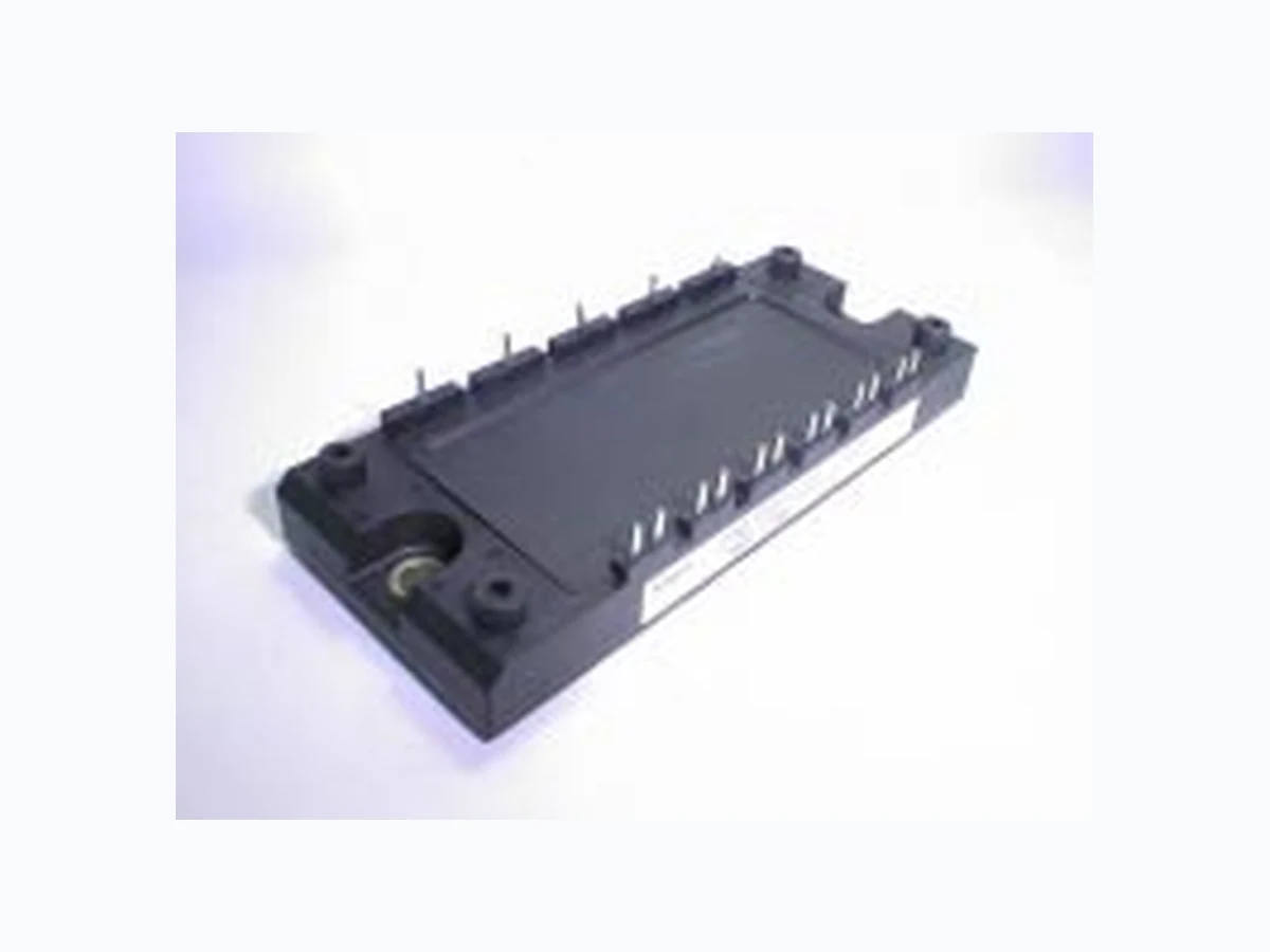
6MBI35S-120 FUJI
Document overview
- Manufacturer or author: Provided By digicamel.com
- PDF pages: 4
Technical content
Features
- Compact package
- P .C.board mount
- Low VCE (sat)
Applications
- Inverter for motor drive
- AC and DC servo drive amplifier
- Uninterruptible power supply
- Industrial machines, such as welding machines
12V15VVGE= 20V Collector current vs. Collector-Emitter voltage Tj= 25 o C (typ.) Collector current : Ic [ A ] Collector - Emitter voltage : VCE [ V ] 012345 10V 12V15VVGE= 20V Collector current vs. Collector-Emitter voltage Tj= 125 o C (typ.) Collector - Emitter voltage : VCE [ V ] Collector current : Ic [ A ] 012345 Tj= 25 o C Tj= 125 o C Collector current vs. Collector-Emitter voltage VGE=15V (typ.) Collector - Emitter voltage : VCE [ V ] Collector current : Ic [ A ] 5 1 01 52 02 5 Ic= 17.5A Ic= 35A Ic= 70A Collector-Emitter voltage vs. Gate-Emitter voltage Tj= 25 o C (typ.) Collector - Emitter voltage : VCE [ V ] Gate - Emitter voltage : VGE [ V ] 0 5 10 15 20 25 30 35 100 1000 10000 Capacitance vs. Collector-Emitter voltage (typ.) VGE=0V, f= 1MHz, Tj= 25 o C Capacitance : Cies, Coes, Cres [ pF ] Collector - Emitter voltage : VCE [ V ] Coes Cres Cies 0 100 200 300 400 200 400 600 800 1000 Dynamic Gate charge (typ.) Vcc=600V, Ic=35A, Tj= 25 o C Gate charge : Qg [ nC ] Collector - Emitter voltage : VCE [ V ] Gate - Emitter voltage : VGE [ V ]
Switching time vs. Collector current (typ.) Switching time : ton, tr, toff, tf [ nsec ] Collector current : Ic [ A ] 02 0 4 0 6 0 100 500 1000 tf tr ton toff Switching time vs. Collector current (typ.) Collector current : Ic [ A ] Switching time : ton, tr, toff, tf [ nsec ] 10 50 100 500 100 500 1000 5000 toff ton tr tf Switching time vs. Gate resistance (typ.) Gate resistance : Rg [ W ] Switching time : ton, tr, toff, tf [ nsec ] 02 0 4 0 6 0 Err(25 o Eoff(25o)C Eon(25 o Err(125 o Eoff(125 o Eon(125 o Switching loss vs. Collector current (typ.) Switching loss : Eon, Eoff, Err [ mJ/pulse ] Collector current : Ic [ A ] 10 50 100 500 Switching loss vs. Gate resistance (typ.) Switching loss : Eon, Eoff, Err [ mJ/pulse ] Gate resistance : Rg [ W ] Eon Err Eoff 0 200 400 600 800 1000 1200 1400 100 Reverse bias safe operating area Collector - Emitter voltage : VCE [ V ] Collector current : Ic [ A ] Vcc=600V,VGE= ±15V, Rg=33 W ,Tj=125oCVcc=600V,VGE= ±15V, Rg=33 W ,Tj=25oC Vcc=600V,VGE= ±15V, Rg=33WVcc=600V,Ic=35A,VGE= ±15V, Tj=25oC =+VGE=15V, -VGE<15V, Rg>33W ,Tj<125oC= =Vcc=600V,Ic=35A,VGE= ±15V,Tj=125oC
Vcc=600V,VGE= ±15V, Rg=33W 107.5–1 93–0.3 69.6–0.3 93–0.3 4-ø6.1–0.3 2-ø5.5–0.3 45–1 41.91 32–0.3 27.6–0.3 + 0.5 3.81 1.15–0.2 ø0.4 ø2.5–0.1 ø2.1–0.1 20.5–1 17–1 3.5–0.5 2.5–0.3 1.5–0.3 6.5–0.5 1–0.2 0.8–0.2 1.5 Section A-A A A 1 12 1317 Shows theory dimensions 16.02 M623 Outline Drawings, mm 01234 Tj=25 o CTj=125 o C Forward current vs. Forward on voltage (typ.) Forward on voltage : VF [ V ] 0 1 02 03 04 05 06 0 100 300 Irr(125 o Irr(25 o trr(25 o trr(125 o Reverse recovery characteristics (typ.) Forward current : IF [ A ] Reverse recovery current : Irr [ A ] Reverse recovery time : trr [ nsec ] 0.001 0.01 0.1 1 0.01 0.1 Transient thermal resistance Thermal resistanse : Rth(j-c) [ o C/W ] Pulse width : Pw [ sec ] FWD IGBT