


 Download PDF
SKY65723-11 SKYWORKS
Document overview
- PDF pages: 11
Technical content
Page 1
DATA SHEET
SKY65723-11: Low-Noise Amplifier Front-End Module with
GPS/GNSS/BDS Pre-Filter
Applications
GPS/GNSS/BDS radio receivers Global Navigation Satellite Systems (GLONASS) Fitness/activity trackers Smartphones Laptop PCs and tablets
Features
Small signal gain: 17 dB typical Low noise figure: 1.8 dB typical Excellent out-of-band rejection Low current consumption Input/output impedance internally matched to 50 Ω Single DC supply: 1.62 to 3.6 V Minimal number of external components required Small MCM (6-pin, 1.7 x 2.3 mm) package (MSL3, 260 C per JEDEC J-STD-020)
Skyworks GreenTM products are compliant with all applicable legislation and are halogen-free. For additional information, refer to Skyworks Definition of GreenTM, document number SQ04–0074.
RF_OUT
RF_IN
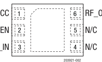
Figure 2. SKY65723-11 Pinout (Top View)
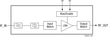
Figure 1. SKY65723-11 Block Diagram
Description
The SKY65723-11 is a front-end module (FEM) with an integrated low-noise amplifier (LNA) and pre-filter designed for Global Positioning System/Global Navigation Satellite System/Beidou Navigation Satellite System (GPS/GNSS/BDS) receiver applications. The device provides high linearity, excellent gain, a high 1 dB input compression point (IP1dB), and a superior noise figure (NF). The pre-filter provides the low in-band insertion loss and integrated notch filtering for excellent rejections of the cellular, PCS, and WLAN frequency bands. The SKY65723-11 uses surface-mount technology (SMT) in the form of a 1.7 x 2.3 mm Multi-Chip Module (MCM) package, which allows for a highly
manufacturable and low-cost solution. An additional filter is incorporated in the SKY65723-11 to improve performance in the presence of a Band 13 blocker. A functional block diagram is shown in Figure 1. The pin configuration and package are shown in Figure 2. Signal pin assignments and functional pin descriptions are provided in Table 1.
Page 2
Table 1. SKY65723-11 Signal Descriptions
| Pin | Name | Description | Pin | Name | Description |
|---|---|---|---|---|---|
| 1 | VCC | Source voltage | 4 | N/C | Not connected or grounded with no impact to performance |
| 2 | VEN | LNA enable | 5 | N/C | Not connected or grounded with no impact to performance |
| 3 | RF_IN | RF input | 6 | RF_OUT | RF output |
Technical Description
LNA Enable
The VEN signal (pin 2) enables or disables the LNA. A logic high signal powers on the LNA and a logic low signal powers off the device.
Table 2. SKY65723-11 Absolute Maximum Ratings1
Electrical and Mechanical Specifications
The absolute maximum ratings of the SKY65723-11 are provided in Table 2. The recommended operating conditions are specified in Table 3, and electrical specifications are provided in Tables 4
and 5.
| Parameter | Symbol | Minimum | Maximum | Units |
|---|---|---|---|---|
| RF input power | PIN | +10 | dBm | |
| Supply voltage | VCC | 0 | 4.5 | V |
| Storage temperature | TSTG | -55 | +150 | C |
| Junction temperature | TJ | +150 | C | |
| Electrostatic discharge: Human Body Model (HBM), Class 1A (at RF_IN pin) | ESD | 250 | V |
1 Exposure to maximum rating conditions for extended periods may reduce device reliability. There is no damage to device with only one parameter set at the limit and all other parameters set at or below their nominal value. Exceeding any of the limits listed here may result in permanent damage to the device.
ESD HANDLING: Although this device is designed to be as robust as possible, electrostatic discharge (ESD) can damage this device.
This device must be protected at all times from ESD when handling or transporting. Static charges may easily produce
potentials of several kilovolts on the human body or equipment, which can discharge without detection.
Industry-standard ESD handling precautions should be used at all times.
Table 3. SKY65723-11 Recommended Operating Conditions
| Parameter | Symbol | Min | Typ | Max | Units |
|---|---|---|---|---|---|
| Frequency range | f | 1559 | 1575 | 1606 | MHz |
| Supply voltage (measured at terminals of Evaluation Board) | VCC | 1.62 | 1.80 | 3.6 | V |
| LNA enable: Enable (high) Disable (low) | LNAENABLE LNADISABLE | VCC - 0.3 | 0 | VCC 0.3 | V V |
| Case operating temperature | TC | -40 | +85 | C |
Page 3
Table 4. SKY65723-11 Electrical Specifications1,2 (f = 1575 MHz, VCC = 1.8 V, VEN = 1.8 V, TC= +25 C, Unless Otherwise Noted)
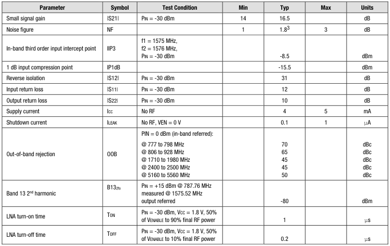
1 Performance is guaranteed only under the conditions listed in this table. 2 Not tested in production. Verified by characterization. 3 0.1 dB has been de-embedded for input connector and trace loss.
Page 4
Table 5. SKY65723-11 Electrical Specifications1 (f = 1575 MHz, VCC = 2.8 V, VEN = 2.8 V, TC= +25 C, Unless Otherwise Noted)
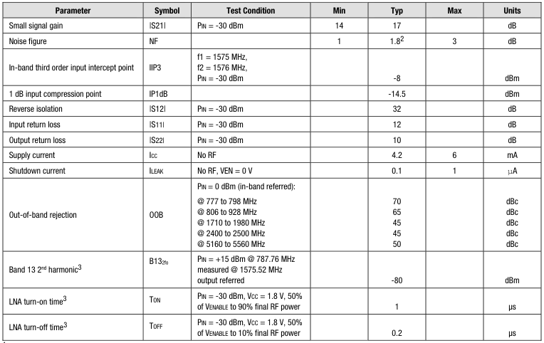
1 Performance is guaranteed only under the conditions listed in this table. 2 0.1 dB has been de-embedded for input connector and trace loss. 3 Not tested in production. Verified by characterization.
Page 5
Evaluation Board Description
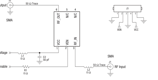
The SKY65723-11 Evaluation Board is used to test the performance of the SKY65723-11 LNA. The Evaluation Board schematic diagram is shown in Figure 3. An assembly drawing for the Evaluation Board is shown in Figure 4. Table 6 provides the Bill of Materials (BOM) list for Evaluation Board components.
Package Dimensions
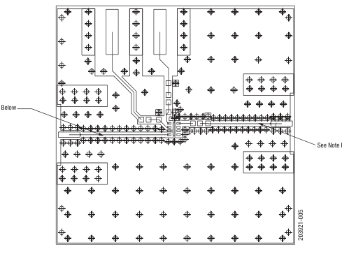
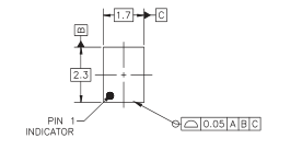
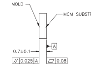
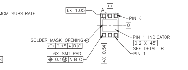
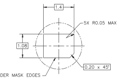
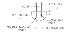
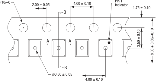
The Evaluation Board layer details for the SKY65723-11 are shown in Figure 5. Layer detail physical characteristics are shown in Figure 6. The PCB layout footprint is provided in Figure 7. Figure 8 shows the typical part marking. Package dimensions are shown in Figure 9, and tape and reel dimensions are provided in Figure 10.
Package and Handling Information
Since the device package is sensitive to moisture absorption, it is baked and vacuum packed before shipping. Instructions on the shipping container label regarding exposure to moisture after the container seal is broken must be followed. Otherwise, problems related to moisture absorption may occur when the part is subjected to high temperature during solder assembly. The SKY65723-11 is rated to Moisture Sensitivity Level 3 (MSL3) at 260 C. It can be used for lead or lead-free soldering. For additional information, refer to the Skyworks Application Note, PCB Design & SMT Assembly/Rework Guidelines for MCM-L Packages, document number 101752. Care must be taken when attaching this product, whether it is
done manually or in a production solder reflow environment. Production quantities of this product are shipped in a standard tape and reel format.
Page 6
J2
RF Output
Source Voltage
LNA Enable
203921-003
Note: DNI components are not shown.
Figure 3. SKY65723-11 Evaluation Board Schematic
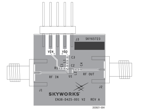
Figure 4. SKY65723-11 Evaluation Board Assembly Diagram
Table 6. SKY65723-11 Evaluation Board Bill of Materials
| Component | Size | Value | Manufacturer | Mfr Part Number |
|---|---|---|---|---|
| C2 | 0402 56 pF | Murata | GRM0335C1E560JA01D | |
| C1, C3, C4 | 0402 DNI | |||
| L1, L2, R1 | 0402 0 Ω | Panasonic | ERJ-2GE0R00X |
Page 7
See Note Below
See Note Below
Figure 5. SKY65723-11 Evaluation Board Layer Details
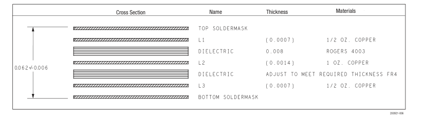
Figure 6. SKY65723-11 Layer Detail Physical Characteristics
Page 8
Stencil aperture size for center
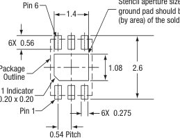
Stencil Aperture
Top View
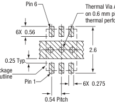
Thermal Via Array, ∅0.3 mm on 0.6 mm pitch improves thermal performance
Package
Metallization
Top View
All dimensions are in millimeters
ground pad should be 80% to 100% (by area) of the solder mask openings
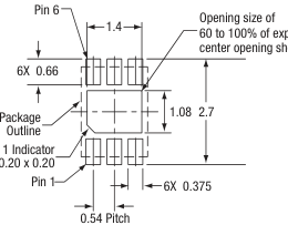
Solder Mask Opening
Top View
203921-007
Figure 7. SKY65723-11 PCB Layout Footprint
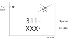
Skyworks Part Number
Figure 8. Typical Part Marking
Page 9
203921-009
Figure 9. SKY65723-11 Package Dimensions
Page 10
∅1.50 +0.10/–0
0.25 ± 0.02
0.90 ± 0.05
Detail B
Notes:
1.85 ± 0.05 (Ao)
- Carrier tape: black conductive polycarbonate. 2. Cover tape material: transparent adhesive material. 3. ESD-surface resistivity is ≥1 x 10⁵ ~ ≤1 x 10⁸ Ohms/square per
5°
EIA, JEDEC TNR Specification. 4. 10-sprocket hole pitch cumulative tolerance: ±0.20 mm.
Detail A
- Ao and Bo measured on plane 0.30 mm above the bottom of pocket.
203921-010
- Camber not to exceed 1 mm in 250 mm. 7. All measurements are in millimeters.
Figure 10. SKY65723-11 Tape and Reel Dimensions
Page 11
Ordering Information
| Product Description | Product Part Number | Evaluation Board Part Number |
|---|---|---|
| SKY65723-11: Low-Noise Amplifier FEM with GPS/GNSS/BDS Filter | SKY65723-11 | 65723-11-EVB |
Copyright © 2016-2017 Skyworks Solutions, Inc. All Rights Reserved.
Information in this document is provided in connection with Skyworks Solutions, Inc. (“Skyworks”) products or services. These materials, including the information contained herein, are provided by Skyworks as a service to its customers and may be used for informational purposes only by the customer. Skyworks assumes no responsibility for errors or omissions in these materials or the information contained herein. Skyworks may change its documentation, products, services, specifications or product descriptions at any time, without notice. Skyworks makes no commitment to update the materials or information and shall have no responsibility whatsoever for conflicts, incompatibilities, or other difficulties arising from any future changes.
No license, whether express, implied, by estoppel or otherwise, is granted to any intellectual property rights by this document. Skyworks assumes no liability for any materials, products or information provided hereunder, including the sale, distribution, reproduction or use of Skyworks products, information or materials, except as may be provided in Skyworks Terms and Conditions of Sale.
THE MATERIALS, PRODUCTS AND INFORMATION ARE PROVIDED “AS IS” WITHOUT WARRANTY OF ANY KIND, WHETHER EXPRESS, IMPLIED, STATUTORY, OR OTHERWISE, INCLUDING FITNESS FOR A PARTICULAR PURPOSE OR USE, MERCHANTABILITY, PERFORMANCE, QUALITY OR NON-INFRINGEMENT OF ANY INTELLECTUAL PROPERTY RIGHT; ALL SUCH WARRANTIES ARE HEREBY EXPRESSLY DISCLAIMED. SKYWORKS DOES NOT WARRANT THE ACCURACY OR COMPLETENESS OF THE INFORMATION, TEXT, GRAPHICS OR OTHER ITEMS CONTAINED WITHIN THESE MATERIALS. SKYWORKS SHALL NOT BE LIABLE FOR ANY DAMAGES, INCLUDING BUT NOT LIMITED TO ANY SPECIAL, INDIRECT, INCIDENTAL, STATUTORY, OR CONSEQUENTIAL DAMAGES, INCLUDING WITHOUT LIMITATION,
LOST REVENUES OR LOST PROFITS THAT MAY RESULT FROM THE USE OF THE MATERIALS OR INFORMATION, WHETHER OR NOT THE RECIPIENT OF MATERIALS HAS BEEN ADVISED OF THE POSSIBILITY OF SUCH DAMAGE.
Skyworks products are not intended for use in medical, lifesaving or life-sustaining applications, or other equipment in which the failure of the Skyworks products could lead to personal injury, death, physical or environmental damage. Skyworks customers using or selling Skyworks products for use in such applications do so at their own risk and agree to fully indemnify Skyworks for any damages resulting from such improper use or sale.
Customers are responsible for their products and applications using Skyworks products, which may deviate from published specifications as a result of design defects, errors, or operation of products outside of published parameters or design specifications. Customers should include design and operating safeguards to minimize these and other risks. Skyworks assumes no liability for applications assistance, customer product design, or damage to any equipment resulting from the use of Skyworks products outside of stated published specifications or parameters.
Skyworks and the Skyworks symbol are trademarks or registered trademarks of Skyworks Solutions, Inc. or its subsidiaries in the United States and other countries. Third-party brands and names are for identification purposes only, and are the property of their respective owners. Additional information, including relevant terms and conditions, posted at www.skyworksinc.com, are incorporated by reference.