

 Download PDF
DATASHEET SEARCH SITE
Document overview
- Manufacturer or author: Provided By www.digicamel.com(FREE DATASHEET DOWNLOAD SITE)
- PDF pages: 7
Technical content
Features
High Speed Current Steering Logic [HCSL] Output Ceramic Surface Mount Package Low Phase Jitter Performance, 500fs Typical Fundamental or 3rd Overtone Crystal Design Frequency Range 13.5MHz – 160MHz * +2.5V or +3.3V Operation Output Enable Standard Tape and Reel Packaging, EIA-418
Applications
PCI Express [PCIe] Data Storage Systems Ethernet Line Cards Serial ATA Express [SATAe] Intel Chipsets Network Servers Switches and Routers Set-Top Boxes/DVRs
Description
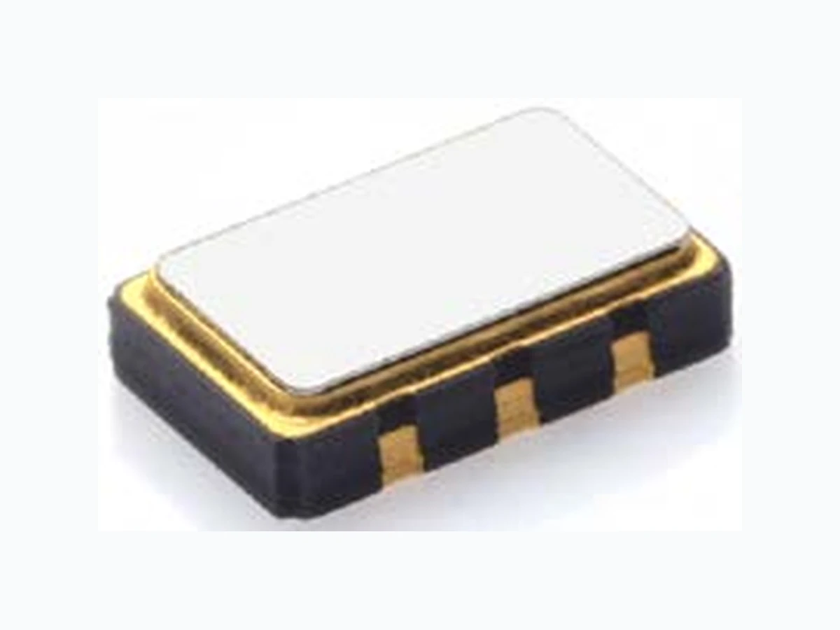
CTS Model 645H is a low cost, high performance clock oscillator supporting HCSL output. Employing the latest IC technology, M645H has excellent stability and low phase jitter performance.
Ordering Information
I G Notes: Contact your local CTS Representative or CTS Customer Service for availability. This product is specified for use only in standard commercial applications. Supplier disclaims all express and implied warranties and liability in connection with any use of this product in any non-commercial applications or in any application that may expose the product to conditions that are outside of the tolerances provided in its specification. Refer to document 016-1454-0, Frequency Code Tables. 3-digits for frequencies <100MHz, 4-digits for frequencies 100MHz or greater. Check factory for availability. Stability codes 2 and 3 only. Not all performance combinations and frequencies may be available. ±100ppm Frequency Temp. Range Packing Product Frequency Code 1 -20°C to +70°C 1k pcs./reel -40°C to +85°C -40°C to +105°C 2 HCSL - Pin 1 Enable ±25ppm +2.5Vdc ±30ppm +3.3Vdc ±50ppm XXX or XXXX 3 I 3 T Output Stability Voltage Output Type Frequency Code [MHz] Frequency Stability Temperature Range Supply Voltage Packaging H Part Dimensions: Standard Frequencies - 25MHz - 100MHz - 155.52MHz - 27MHz - 106.25MHz - 156.25MHz - 50MHz - 125MHz * Check with factory for availability of frequencies not listed.
©2017 CTS® Corporation. Information/product(s) subject to change. No warranty that product(s) will meet the stated specifications for customer specific applications or test equipment. Visit www.ctscorp.com for list of applicable patent(s), more information, or to request a quote. Model 645H Very Low Jitter HCSL Clock DOC# 008-0582-1 Rev. C Page 2 of 7 Electrical Specifications Operating Conditions PARAMETER SYMBOL CONDITIONS MIN TYP MAX UNIT Maximum Supply Voltage VCC - -0.3 - 4.0 V 2.375 2.5 2.625 3.135 3.3 3.465 Supply Current ICC Maximum Load Maximum Current Value @ +3.3V - - 60 mA -20 +70 -40 +85 -40 +105 Storage Temperature TSTG - -50 - +125 °C Frequency Stability PARAMETER SYMBOL CONDITIONS MIN TYP MAX UNIT Frequency Range fO - MHz Frequency Stability [Note 1] Δf/fO - ±ppm Aging Δf/f25 First Year @ +25°C, nominal VCC -5 ±3 5 ppm Output Parameters PARAMETER SYMBOL CONDITIONS MIN TYP MAX UNIT Output Type - - - Output Load RL Terminated to ground - 50 - Ohms VOH -580 - 850 VOL -150 - 150 Output Duty Cycle SYM Differential Output, @ VCC - 1.3V 45 - 55 % Differential Output Voltage VOD RL = 50 Ohms to ground 0.4 - - Vp-p Rise and Fall Time TR, TF @ 20%/80% Levels, RL = 50 Ohms to ground - 0.50 0.70 ns Output Parameters PARAMETER SYMBOL CONDITIONS MIN TYP MAX UNIT Start Up Time TS Application of VCC - 5 10 ms Enable Function [Standby] Enable Input Voltage VIH Pin 1 Logic '1', Output Enabled 0.7VCC - - V Disable Input Voltage VIL Pin 1 Logic '0', Output Disabled - - 0.3VCC V Disable Current IIL Pin 1 Logic '0', Output Disabled - 15 - µA Enable Time TPLZ Pin 1 Logic '1', Output Enabled - - 2 ms Phase Jitter, RMS tjrms Bandwidth 12 kHz - 20 MHz - 500 - fs Supply Voltage VCC ±5% V Operating Temperature TA - +25 °C 13.5 - 160 25, 30, 50 or 100 1.] Inclusive of initial tolerance at time of shipment, changes in supply voltage, load, temperature and 1st year aging. HCSL Output Voltage Levels HCSL Load mV
©2017 CTS® Corporation. Information/product(s) subject to change. No warranty that product(s) will meet the stated specifications for customer specific applications or test equipment. Visit www.ctscorp.com for list of applicable patent(s), more information, or to request a quote. Model 645H Very Low Jitter HCSL Clock DOC# 008-0582-1 Rev. C Page 3 of 7 Electrical Specifications Enable Truth Table Pin 1 Pin 4 & Pin 5 Logic ‘1’ Output Open Output Logic ‘0’ High Imp. Test Circuit HCSL Output Waveform HCSL
©2017 CTS® Corporation. Information/product(s) subject to change. No warranty that product(s) will meet the stated specifications for customer specific applications or test equipment. Visit www.ctscorp.com for list of applicable patent(s), more information, or to request a quote. Model 645H Very Low Jitter HCSL Clock DOC# 008-0582-1 Rev. C Page 4 of 7 Electrical Specifications Performance Data Phase Noise [typical] 100.00MHz, HCSL, VCC = 3.3V, TA = +25°C
©2017 CTS® Corporation. Information/product(s) subject to change. No warranty that product(s) will meet the stated specifications for customer specific applications or test equipment. Visit www.ctscorp.com for list of applicable patent(s), more information, or to request a quote. Model 645H Very Low Jitter HCSL Clock DOC# 008-0582-1 Rev. C Page 5 of 7 Electrical Specifications Performance Data Phase Noise Tabulated Typical, 100.00MHz, HCSL, VCC = 3.3V, TA = +25°C PARAMETER SYMBOL CONDITIONS TYP UNIT HCSL @ 100.00MHz Phase Noise Single Side Band @ 10Hz -75.9328 @ 100Hz -106.9929 @ 1kHz -135.1951 @ 10kHz -144.2209 @ 100kHz -152.8159 @ 1MHz -153.5793 @ 10MHz -154.8219 Phase Jitter, RMS tjrms Integration Bandwidth 12kHz - 20MHz 188.2315 fs - dBc/Hz
©2017 CTS® Corporation. Information/product(s) subject to change. No warranty that product(s) will meet the stated specifications for customer specific applications or test equipment. Visit www.ctscorp.com for list of applicable patent(s), more information, or to request a quote. Model 645H Very Low Jitter HCSL Clock DOC# 008-0582-1 Rev. C Page 6 of 7 Mechanical Specifications Package Drawing Marking Information Recommended Pad Layout Notes Pin Assignments Pin Symbol Function
1 EOH Enable
2 N.C. No Connect
3 GND Circuit & Package Ground
4 Output RF Output
5 N.C. No Connect
6 VCC Supply Voltage
2001 2005 2009 2013 2017 A B C D E F G H J K L M 2002 2006 2010 2014 2018 N P Q R S T U V W X Y Z 2003 2007 2011 2015 2019 a b c d e f g h j k l m 2004 2008 2012 2016 2020 n p q r s t u v w x y z NOV DECYEAR MAY JUN JUL AUG SEP OCTMONTH JAN FEB MAR APR 1. O – Output Type; H = HCSL. 2. ST – Frequency Stability/Temperature Code. [Refer to Ordering Information] 3. V – Voltage Code; 3 = 3.3V, 2 = 2.5V. 4. D – Date Code. See Table I for codes. 5. xxxx – Frequency Code. 3-digits, frequencies below 100MHz 4-digits, frequencies 100MHz or greater [See document 016-1454-0, Frequency Code Tables.] 1. JEDEC termination code (e4). Barrier-plating is nickel [Ni] with gold [Au] flash plate. 2. Reflow conditions per JEDEC J-STD-020; +260°C maximum, 20 seconds. 3. MSL = 1. 645OSTV
- Dxxxx
©2017 CTS® Corporation. Information/product(s) subject to change. No warranty that product(s) will meet the stated specifications for customer specific applications or test equipment. Visit www.ctscorp.com for list of applicable patent(s), more information, or to request a quote. Model 645H Very Low Jitter HCSL Clock DOC# 008-0582-1 Rev. C Page 7 of 7 Packaging - Tape and Reel Tape Drawing Reel Drawing Notes 1. Device quantity is 1k pieces maximum per 180mm reel. 2. Complete CTS part number, frequency value and date code information must appear on reel and carton labels.