
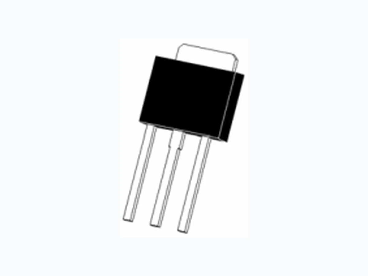
630A ETC
Document overview
- Manufacturer or author: Provided By www.digicamel.com(free datasheet download site)
- PDF pages: 6
Technical content
Features
- Fast switching
- 100% avalanche tested
- Improved dv/dt capability Application DC Motor Control and Class D Amplifier
- Uninterruptible Power Supply (UPS) Automotive Page V D S S R D S O N I D 0.21 A 10V @ (typ) Ω200V TO -252 TO-251 630A GOFORD HTTP://www.gofordsemi.com T E L 961262 F A X
Symbol Parameter Test Condition Min. Typ. Max. Unit s Off Characteristic V (BR)DSS Drain-Source Breakdown Voltage V GS = 0V,I D = 250µA 200 - - V (BR)DSS /△T J Breakdown Voltage Temperature Coefficient Reference to 25℃, I D = 250µA - 0.25 - V/℃ V DS = 200V, V GS = 0V - - 1 µA I DSS Zero Gate Voltage Drain Current V DS = 160V, T C = 125℃ - - 10 µA I GSS Gate to Body Leakage Current V DS = 0V, V GS = ±30V - - ±100 nA On Characteristics V GS(th) Gate Threshold Voltage note4 V DS = V GS , I D = 250µ R DS(on) Static Drain-Source On-Resistance V GS =10V, I D = 4.5A - 0.21 0.25 Ω g FS Forward Transconductance V DS =30V, I D = 4.5A - 9.2 - S Dynamic Characteristics C iss Input Capacitance - 509 - pF C oss Output Capacitance - 51.5 - pF C rss Reverse Transfer Capacitance V DS = 25V, V GS = 0V, f = 1.0MHz - 3.2 - pF Q g Total Gate Charge - 11.8 - nC Q gs Gate-Source Charge - 2.36 - nC Q gd Gate-Drain(“Miller”) Charge VDD = 160V, ID = 9A, V GS = 10V - 3.98 - nC Switching Characteristics t d(on) Turn-On Delay Time - 10.33 - ns t r Turn-On Rise Time - 10.7 - ns t d(off) Turn-Off Delay Time - 29.1 - ns t f Turn-Off Fall Time V DD = 100V, I D = 9A, RG = 10Ω, VGS = 10V - 11.1 - ns Drain-Source Diode Characteristics and Maximum Ratings I S Maximum Continuous Drain to Source Diode Forward Current - - 9 A I SM Maximum Pulsed Drain to Source Diode Forward Curre nt - - 36 A V SD Drain to Source Diode Forward Voltage V GS = 0V, I S = 9A - - 1.4 V t rr Reverse Recovery Time - 201 - ns Q rr Reverse Recovery Charge V GS = 0V, I F = 9A, di/dt =100A/µs - 663 - nC Notes: 1. Repetitive Rating: Pulse width limited by maximum junction temperature 2. L = 10mH, I AS = 8A, V DD = 50V, R G = 25Ω, Starting T J = 25° C 3. I SD ≤ 9A, di/dt ≤ 200A/µs, V DD ≤ B VDSS , Starting T J = 25° C 4. Pulse width ≤ 300µs; duty cycle ≤ 2%. Page
Electrical Characteristics
T C =25℃ unless otherwise specified 630A GOFORD HTTP://www.gofordsemi.com T E L 961262 F A X A 1 1.8 2.5 V
Figure 15. Peak Diode Recovery dv/dt Test Circuit & Waveforms (For N-channel)