
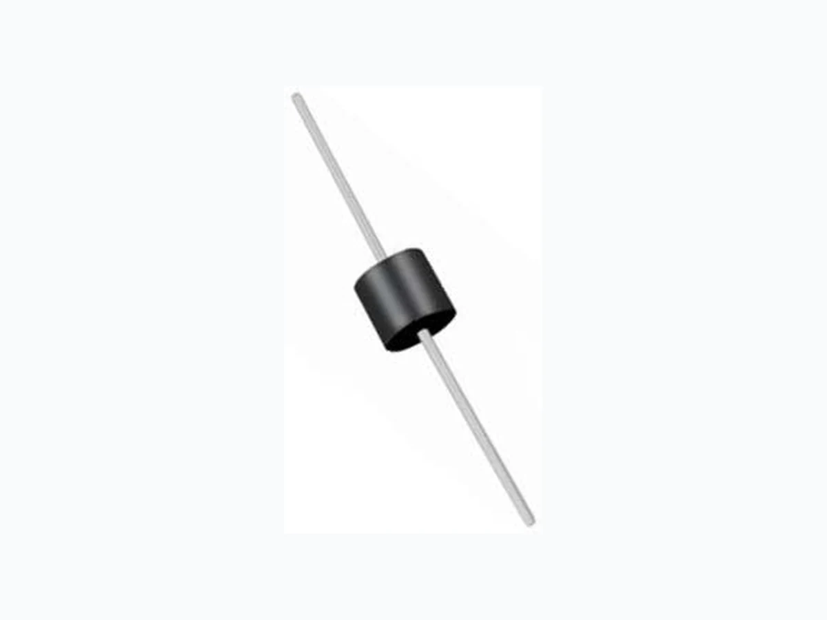
5KP5.0E3 MICROSEMI
Document overview
- Manufacturer or author: Provided By digicamel.com
- PDF pages: 10
Technical content
RF01010-1, Rev. A (9/13/13) ©2013 Microsemi Corporation Page 1 of 10 5KP5.0e3 – 5KP250CAe3 Compliant 5,000 Watt Transient Voltage Suppressor (TVS) Protection Device
DESCRIPTION
This RoHS compliant transient voltage suppressor series 5KP5.0e3 - 5KP250CAe3 provides a range of standoff voltage options from 5.0 to 250V in both unidirectional and bidirectional options. Clamping action is almost instantaneous. As a result, they provide effective protection from ESD and EFT per IEC61000-4-2 and IEC61000-4-4, as well as transients caused by inductive switching and RFI. They also protect from secondary lightning effects per 61000-4-5 at the class levels specified below. Also available in: Case 5A (DO-204AR) package (hirel plastic axial-leaded) M5KP5.0A – M5KP110CA DO-13 package (metal axial-leaded) LC6.5A – LC170A Important: For the latest information, visit our website http://www.microsemi.com.
FEATURES
- Available in both unidirectional and bidirectional configurations
- Moisture classification is level 1 with no dry pack required per IPC/JEDEC J-STD-020B
- RoHS compliant APPLICATIONS / BENEFITS
- Selections for 5.0 to 250 volts stand-off voltage (VWM)
- Economical TVS series for thru-hole mounting
- Pico- to nano-second response time
- Protection from transients caused by inductive switching and RFI
- Compliant to IEC 61000-4-2 and IEC 61000-4-4 for ESD and EFT protection respectively
- Secondary lightning protection per IEC61000-4-5 with 42 ohms source impedance: Class 1, 2, 3, 4: 5KP5.0 to 5KP110CA Class 5: 5KP5.0 to 5KP110CA (short distance) Class 5: 5KP5.0 to 5KP36CA (long distance)
- Secondary lightning protection per IEC61000-4-5 with 12 ohms source impedance: Class 1 & 2: 5KP5.0 to 5KP110CA Class 3: 5KP5.0 to 5KP78CA Class 4: 5KP5.0 to 5KP40CA
- Secondary lightning protection per IEC61000-4-5 with 2 ohms source impedance: Class 2: 5KP5.0 to 5KP70CA Class 3: 5KP5.0 to 5KP36CA Class 4: 5KP5.0 to 5KP18CA MSC – Lawrence
6 Lake Street,
Lawrence, MA 01841 1-800-446-1158 or (978) 620-2600 Fax: (978) 689-0803 MSC – Ireland Gort Road Business Park, Ennis, Co. Clare, Ireland Tel: +353 (0) 65 6840044 Fax: +353 (0) 65 6822298 Website: www.microsemi.com
RF01010-1, Rev. A (9/13/13) ©2013 Microsemi Corporation Page 2 of 10 5KP5.0e3 – 5KP250CAe3 MAXIMUM RATINGS @ 25 ºC unless otherwise noted Parameters/Test Conditions Symbol Value Unit Junction and Storage Temperature TJ and TSTG -55 to +175 oC Thermal Resistance, Junction to Lead @ 0.375 inch (9.5 mm) lead length from body RӨJL 8.0 oC/W Thermal Resistance, Junction to Ambient RӨJA 40 oC/W Peak Pulse Power Dissipation 10/1000 µs PPP 5000 W Rated Average Power Dissipation @ TL = 75 ºC 0.375 inch (9.5 mm) from body (1) PM(AV) 8.0 W Surge Peak Forward Current (2) IFSM 500 A Solder Temperature @ 10 s 260 oC Notes: 1. When mounted as sho wn in Figure 5 2. Measured on 8.3ms single half sine -wave or equivalent square wave, duty cycle = 4 pulses per minute maximum MECHANICAL and PACKAGING
- CASE: Void-free transfer molded thermosetting epoxy body meeting UL94V-0
- TERMINALS: RoHS compliant annealed matte-tin plating. Solderable per MIL-STD-750, method 2026.
- MARKING: Manufacturer, date code, part number, polarity and tolerance suffixes
- POLARITY: For unidirectional types the color band denotes the cathode, which is positive with respect to the anode under normal TVS operation.
- TAPE & REEL option: Standard per EIA-296 (add “TR” suffix to part number). Consult factory for quantities.
- WEIGHT: Approximately 2.1 grams
- See Package Dimensions on last page. PART NOMENCLATURE 5K P 5.0 C A e3
5 Kilowatt Rating
(see Electrical Characteristics table) RoHS Compliant Voltage Tolerance A = 5% tolerance level Blank = 10% tolerance Polarity C = Bidirectional Blank = Unidirectional
RF01010-1, Rev. A (9/13/13) ©2013 Microsemi Corporation Page 3 of 10 5KP5.0e3 – 5KP250CAe3 SYMBOLS & DEFINITIONS Symbol Definition αV(BR) Temperature Coefficient of Breakdown Voltage: The change in breakdown voltage divided by the change in temperature that caused it expressed in %/°C or mV/°C. ID Standby Current: The current through the device at rated stand-off voltage. IPP Peak Impulse Current: The maximum rated random recurring peak impulse current or nonrepetitive peak impulse current that may be applied to a device. A random recurring or nonrepetitive transient current is usually due to an external cause, and it is assumed that its effect will have completely disappeared before the next transient arrives. PPP Peak Pulse Power. The rated random recurring peak impulse power or rated nonrepetitive peak impulse power. The impulse power is the maximum-rated value of the product of IPP and VC. V(BR) Breakdown Voltage: The voltage across the device at a specified current I(BR) in the breakdown region. VC Clamping Voltage: The voltage across the device in a region of low differential resistance during the application of an impulse current (IPP) for a specified waveform. VWM Working Standoff Voltage: The maximum-rated value of dc or repetitive peak positive cathode-to-anode voltage that may be continuously applied over the standard operating temperature.
RF01010-1, Rev. A (9/13/13) ©2013 Microsemi Corporation Page 4 of 10 5KP5.0e3 – 5KP250CAe3 ELECTRICAL CHARACTERISTICS @ 25 ºC unless otherwise stated DEVICE NUMBER BREAKDOWN VOLTAGE (1) BR V( BR) @ IT TEST CURRENT IT WORKING STAND- OFF VOLTAGE VWM MAXIMUM STANDBY CURRENT (3) ID @ VWM MAXIMUM PEAK PULSE CURRENT (2) IPP MAXIMUM CLAMPING VOLTAGE VC @ IPP MAXIMUM TEMPERATURE COEFFICIENT OF V( BR) αV(BR) Min Max Volts mA mA Volts µA Amps Volts %/ºC 5KP10e3 / 5KP10Ce3 11.1 13.6 5 10 15 266 18.8 0.084 5KP10Ae3 / 5KP10CAe3 11.1 12.3 5 10 15 294 17.0 0.084 5KP11e3 / 5KP11Ce3 12.2 14.9 5 11 10 249 20.1 0.086 5KP11Ae3 / 5KP11CAe3 12.2 13.5 5 11 10 275 18.2 0.086 5KP12e3 / 5KP12Ce3 13.3 16.3 5 12 5 227 22.0 0.088 5KP12Ae3 / 5KP12CAe3 13.3 14.7 5 12 5 251 19.9 0.088 5KP13e3 / 5KP13Ce3 14.4 17.6 5 13 2 210 23.8 0.090 5KP13Ae3 / 5KP13CAe3 14.4 15.9 5 13 2 233 21.5 0.090 5KP14e3 / 5KP14Ce3 15.6 19.1 5 14 2 194 25.8 0.092 5KP14Ae3 / 5KP14CAe3 15.6 17.2 5 14 2 216 23.2 0.092 5KP15e3 / 5KP15Ce3 16.7 20.4 5 15 2 186 26.9 0.094 5KP15Ae3 / 5KP15CAe3 16.7 18.5 5 15 2 205 24.4 0.094 5KP16e3 / 5KP16Ce3 17.8 21.8 5 16 2 174 28.8 0.096 5KP16Ae3 / 5KP16CAe3 17.8 19.7 5 16 2 192 26.0 0.096 5KP17e3 / 5KP17Ce3 18.9 23.1 5 17 2 164 30.5 0.097 5KP17Ae3 / 5KP17CAe3 18.9 20.9 5 17 2 181 27.6 0.097 5KP18e3 / 5KP18Ce3 20.0 24.4 5 18 2 155 32.2 0.098 5KP18Ae3 / 5KP18CAe3 20.0 22.1 5 18 2 171 29.2 0.098 5KP20e3 / 5KP20Ce3 22.2 27.1 5 20 2 140 35.8 0.099 5KP20Ae3 / 5KP20CAe3 22.2 24.5 5 20 2 154 32.4 0.099 5KP22e3 / 5KP22Ce3 24.4 29.8 5 22 2 127 39.4 0.100 5KP22Ae3 / 5KP22CAe3 24.4 26.9 5 22 2 141 35.5 0.100 5KP24e3 / 5KP24Ce3 26.7 32.6 5 24 2 116 43.0 0.101 5KP24Ae3 / 5KP24CAe3 26.7 29.5 5 24 2 129 38.9 0.101 Continued on next page
RF01010-1, Rev. A (9/13/13) ©2013 Microsemi Corporation Page 5 of 10 5KP5.0e3 – 5KP250CAe3 ELECTRICAL CHARACTERISTICS @ 25 ºC unless otherwise stated (continued) DEVICE NUMBER BREAKDOWN VOLTAGE (1) BR V( BR) @ IT TEST CURRENT IT STAND- OFF VOLTAGE VWM MAXIMUM STANDBY CURRENT (3) ID @ VWM MAXIMUM PEAK PULSE CURRENT (2) IPP MAXIMUM CLAMPING VOLTAGE VC @ IPP MAXIMUM TEMPERATURE COEFFICIENT OF V( BR) αV(BR) Min Max Volts mA mA Volts µA Amps Volts %/ºC 5KP26e3 / 5KP26Ce3 28.9 35.3 5 26 2 107 46.6 0.101 5KP26Ae3 / 5KP26CAe3 28.9 31.9 5 26 2 119 42.1 0.101 5KP28e3 / 5KP28Ce3 31.1 38.0 5 28 2 100 50.0 0.102 5KP28Ae3 / 5KP28CAe3 31.1 34.4 5 28 2 110 45.4 0.102 5KP30Ae3 / 5KP30CAe3 33.3 36.8 5 30 2 103 48.4 0.103 5KP58e3 / 5KP58Ce3 64.4 78.7 5 58 2 48.5 103 0.107 5KP58Ae3 / 5KP58CAe3 64.4 71.2 5 58 2 53.4 94 0.107 5KP60e3 / 5KP60Ce3 66.7 81.5 5 60 2 46.7 107 0.108 5KP60Ae3 / 5KP60CAe3 66.7 73.7 5 60 2 51.7 97 0.108 5KP64e3 / 5KP64Ce3 71.1 86.9 5 64 2 43.9 114 0.108 5KP64Ae3 / 5KP64CAe3 71.1 78.6 5 64 2 48.5 103 0.108 5KP70e3 / 5KP70Ce3 77.8 95.1 5 70 2 40.0 125 0.108 5KP70Ae3 / 5KP70CAe3 77.8 86.0 5 70 2 44.2 113 0.108 5KP75e3 / 5KP75Ce3 83.3 102 5 75 2 37.3 134 0.108 5KP75Ae3 / 5KP75CAe3 83.3 92.1 5 75 2 41.3 121 0.108 5KP78e3 / 5KP78Ce3 86.7 106 5 78 2 36.0 139 0.108 5KP78Ae3 / 5KP78CAe3 86.7 95.8 5 78 2 39.7 126 0.108 5KP85e3 / 5KP85Ce3 94.4 115 5 85 2 33.1 151 0.108 5KP85Ae3 / 5KP85CAe3 94.4 104 5 85 2 36.5 137 0.108 5KP90e3 / 5KP90Ce3 100 122 5 90 2 31.3 160 0.110 5KP90Ae3 / 5KP90CAe3 100 111 5 90 2 34.2 146 0.110 5KP100e3 / 5KP100Ce3 111 136 5 100 2 27.9 179 0.110 5KP100Ae3 / 5KP100CAe3 111 123 5 100 2 30.9 162 0.110 Continued on next page
RF01010-1, Rev. A (9/13/13) ©2013 Microsemi Corporation Page 6 of 10 5KP5.0e3 – 5KP250CAe3 ELECTRICAL CHARACTERISTICS @ 25 ºC unless otherwise stated (continued) DEVICE NUMBER BREAKDOWN VOLTAGE (1) BR V( BR) @ IT TEST CURRENT IT STAND- OFF VOLTAGE VWM MAXIMUM STANDBY CURRENT (3) ID @ VWM MAXIMUM PEAK PULSE CURRENT (2) IPP MAXIMUM CLAMPING VOLTAGE VC @ IPP MAXIMUM TEMPERATURE COEFFICIENT OF V( BR) αV(BR) Min Max Volts mA mA Volts µA Amps Volts %/ºC 5KP110e3 / 5KP110Ce3 122 149 5 110 2 25.5 196 0.110 5KP110Ae3 / 5KP110CAe3 122 135 5 110 2 28.2 177 0.110 5KP120e3 / 5KP120Ce3 133 162 5 120 2 23.5 213 0.110 5KP120Ae3 / 5KP120CAe3 133 147 5 120 2 26.4 193 0.110 5KP130e3 / 5KP130Ce3 144 175 5 130 2 21.6 231 0.110 5KP130Ae3 / 5KP130CAe3 144 159 5 130 2 24.4 209 0.110 5KP150e3 / 5KP150Ce3 167 204 5 150 2 18.7 268 0.110 5KP150Ae3 / 5KP150CAe3 167 185 5 150 2 21.0 243 0.110 5KP160e3 / 5KP160Ce3 178 217 5 160 2 17.4 287 0.110 5KP160Ae3 / 5KP160CAe3 178 197 5 160 2 19.7 259 0.110 5KP170e3 / 5KP170Ce3 189 231 5 170 2 16.4 304 0.110 5KP170Ae3 / 5KP170CAe3 189 209 5 170 2 18.5 275 0.110 5KP180e3 / 5KP180Ce3 200 244 5 180 2 15.5 323 0.110 5KP180Ae3 / 5KP180CAe3 200 221 5 180 2 17.5 292 0.110 5KP190e3 / 5KP190Ce3 211 258 5 190 2 14.6 343 0.110 5KP190Ae3 / 5KP190CAe3 211 233 5 190 2 16.5 310 0.110 5KP200e3 / 5KP200Ce3 222 271 5 200 2 13.7 364 0.110 5KP200Ae3 / 5KP200CAe3 222 246 5 200 2 15.5 329 0.110 5KP210e3 / 5KP210Ce3 233 284 5 210 2 12.9 386 0.110 5KP210Ae3 / 5KP210CAe3 233 258 5 210 2 14.6 349 0.110 5KP220e3 / 5KP220Ce3 244 298 5 220 2 12.2 410 0.110 5KP220Ae3 / 5KP220CAe3 244 270 5 220 2 13.7 371 0.110 5KP250e3 / 5KP250Ce3 277 338 5 250 2 10.6 470 0.110 5KP250Ae3 / 5KP250CAe3 277 306 5 250 2 12.0 425 0.110 NOTES: (1) V(BR) measured after IT applied for 300 µs, IT = square wave pulse or equivalent (2) Surge current waveform per Figure 3 and derated per Figure 2 (3) For bidrectional types with V WM of 30 volts and less, the I D limit is doubled
RF01010-1, Rev. A (9/13/13) ©2013 Microsemi Corporation Page 10 of 10 5KP5.0e3 – 5KP250CAe3 PACKAGE DIMENSIONS Dimensions Dim Inch Millimeters Min Max Min Max LL 0.750 - 19.05 - BL 0.340 0.360 8.645 9.135 BD 0.340 0.360 8.645 9.135 LD 0.047 0.053 1.194 1.346