
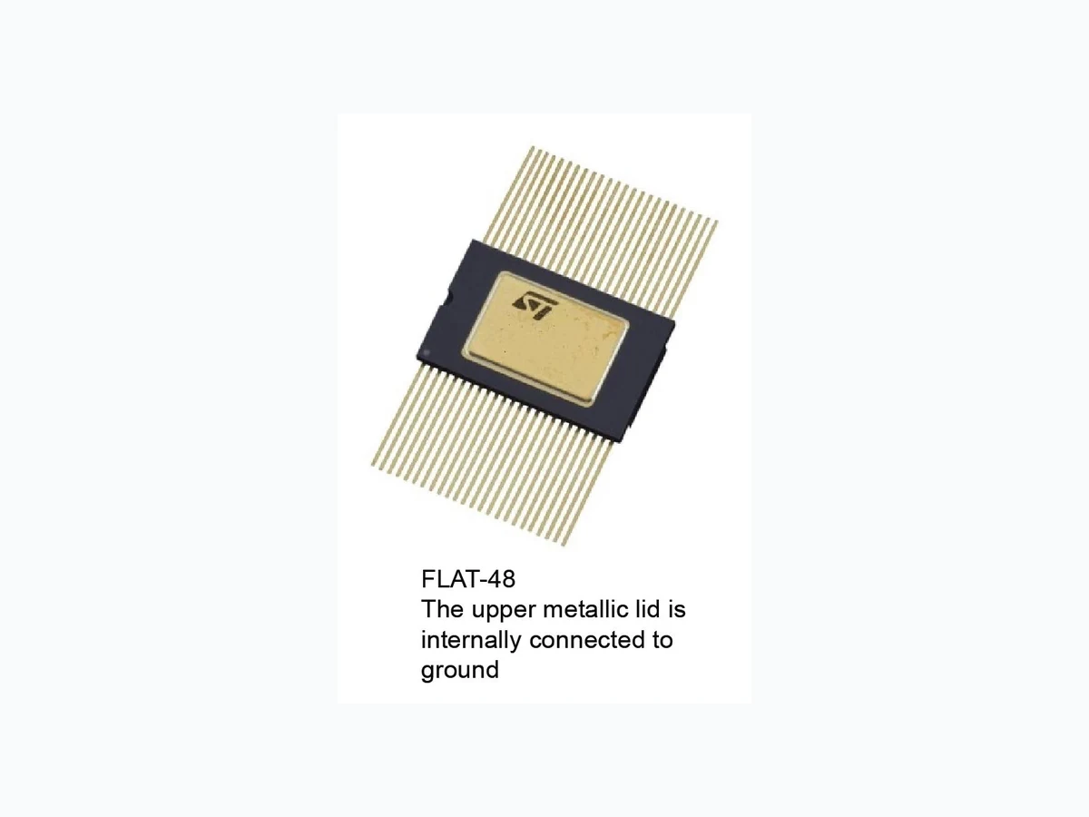
Datasheet - 54VCXH162244 - Low voltage CMOS 16-bit bus buffer (3-state non inverter) with 3.6 V tolerant inputs and outputs
Document overview
- Manufacturer or author: STMICROELECTRONICS
- PDF pages: 20
Technical content
Datasheet sections
- 1 Logic symbols and I/O equivalent circuit
- 2 Pin settings
- 2.1 Pin connection
- 2.2 Pin description
- 2.3 Truth table
- 3 Maximum ratings
- 3.1 Recommended conditions
- 4 Electrical characteristics
- 5 Test circuit
- 6 Waveforms
- 7 Package information
- 7.1 FLAT-48 package information
- 8 Ordering information
Features
- 1.8 to 3.6 V operating voltage
- 5 ns propagation delay
- 100 mV typical input hysteresis
- Power down protection on inputs and outputs
- Symmetrical output impedance
- 26 Ω series resistance in outputs
- Bus hold on data inputs
- Cold spare function
- Latch-up performance exceeds 300 mA (JESD 17)
- 300 krad(Si) total ionizing dose (TID)
- No SEL, no SEU and no SET at 110 MeV.cm2/mg LET
- QML-V qualified
- SMD 5962F05210
Description
The 54VCXH162244 is a low voltage CMOS 16-bit bus buffer (non inverted) fabricated with submicron silicon gate and five-layer metal wiring C²MOS technology. It is ideal for low power and very high speed 1.8 V to 3.6 V applications; it can be interfaced to 3.6 V signal environment for both inputs and outputs. Any nG output control governs four BUS buffers. Output enable input (nG) tied together gives full 16- bit operation. When nG is low, the outputs are on. When nG is high, the output are in high impedance state. This device is designed to be used with 3-state memory address drivers, etc. Bus hold on data inputs is provided in order to eliminate the need for external pull-up or pull-down resistor. The device circuits is including 26 Ω series resistance in the outputs. These resistors permit to reduce line noise in high speed applications. All inputs and outputs are equipped with protection circuits against static discharge, giving them 2 kV ESD immunity and transient excess voltage. Product status link 54VCXH162244 Low voltage CMOS 16-bit bus buffer (3-state non inverter) with 3.6 V tolerant inputs and outputs 54VCXH162244 Datasheet DS3953 - Rev 11 - January 2024 For further information contact your local STMicroelectronics sales office.
1 Logic symbols and I/O equivalent circuit
Figure 1. IEC logic symbols
Figure 2. Input and output equivalent circuit
2 Pin settings
2.1 Pin connection
Figure 3. Pin connection (top through view)
2.2 Pin description
Table 1. Pin description
2.3 Truth table
Table 2. Truth table
3 Maximum ratings
rating conditions for extended periods may affect device reliability. Table 3. Absolute maximum ratings
- IO absolute maximum rating must be observed.
- Short-circuits can cause excessive heating and destructive dissipation. Values are typical.
- Human body model: a 100 pF capacitor is charged to the specified voltage, then discharged through a 1.5 kΩ resistor
between two pins of the device. This is done for all couples of connected pin combinations while the other pins are floating.
3.1 Recommended conditions
Table 4. Recommended operating conditions
4 Electrical characteristics
Table 5. DC specifications Table 6. DC specifications
Electrical characteristics
Table 7. Dynamic switching characteristics
- Number of outputs defined as “n”. Measured with “n-1” output switching from HIGH to LOW or LOW to HIGH. The remaining
output is measured in the LOW state.
- Parameters guaranteed by design.
- Number of outputs defined as “n”. Measured with “n-1” outputs switching from HIGH to LOW or LOW to HIGH. The
remaining output is measured in the HIGH state. Table 8. AC electrical characteristics Table 9. Capacitive characteristics
- CPD is defined as the value of the IC’s internal equivalent capacitance which is calculated from the operating current
consumption without load. (Refer to test circuit). Average operating current can be obtained by the following equation. ICC(opr) = CPD x VCC x fIN + ICC/16 (per circuit).
5 Test circuit
Figure 4. Application circuit Table 10. Test circuit
6 Waveforms
Figure 5. Waveform - propagation delay (f = 1 MHz; 50% duty cycle) Figure 6. Waveform - output enable and disable time (f = 1 MHz; 50% duty cycle)
7 Package information
In order to meet environmental requirements, ST offers these devices in different grades of ECOPACK packages, depending on their level of environmental compliance. ECOPACK specifications, grade definitions and product status are available at: www.st.com. ECOPACK is an ST trademark.
7.1 FLAT-48 package information
Figure 7. FLAT-48 package outline
Package information
DS3953 - Rev 11 page 12/20
Table 11. FLAT-48 package mechanical data
- Values in inches are converted from mm and rounded to 4 decimal digits.
DS3953 - Rev 11 page 13/20
8 Ordering information
Order code SMD (1) Qualification level Mass Package Lead finish Marking (2) Packing RHFXH162244K1 - Engineering model 1.5 g Flat-48 Gold RHFXH162244K1 Conductive strip packRHFXH162244K03V 5962F05210 QML-V Flight 5962F0521002VXC RHFXH162244K05V 5962F05210 QML-V Flight Flat-48 with grounded lid 5962F0521002VYC 1. Standard microcircuit drawing 2. Specific marking only. Complete marking includes the following:
- ST logo
- Date code (date the package was sealed) in YYWWA (year, week, and lot index of week) Other information Date code: The date code is structured as engineering model: EM xyywwz Where: x = 3 (EM only), assembly location Rennes (France) yy = last two digits of the year ww = week digits z = lot index of the week Product documentation Each product shipment includes a set of associated documentation within the shipment box. This documentation depends on the quality level of the products, as detailed in the table below. The certificate of conformance is provided on paper whatever the quality level. For QML parts, complete documentation, including the certificate of conformance, is provided on a CDROM.
Table 12. Product documentation
Ordering information
DS3953 - Rev 11 page 14/20
Reference to the applicable SMD ST Rennes assembly lot ID Quality control inspection (groups A, B, C, D, E) Screening electrical data in/out summary Precap report PIND (particle impact noise detection) test SEM (scanning electronic microscope) inspection report X-ray plates 54VCXH162244 DS3953 - Rev 11 page 15/20
Revision history
Table 13. Document revision history 09-Jul-2004 1 Initial release. Updated figure and features on the cover page. Section 8: Ordering information.
IMPORTANT NOTICE – READ CAREFULLY STMicroelectronics NV and its subsidiaries (“ST”) reserve the right to make changes, corrections, enhancements, modifications, and improvements to ST products and/or to this document at any time without notice. Purchasers should obtain the latest relevant information on ST products before placing orders. ST products are sold pursuant to ST’s terms and conditions of sale in place at the time of order acknowledgment. Purchasers are solely responsible for the choice, selection, and use of ST products and ST assumes no liability for application assistance or the design of purchasers’ products. No license, express or implied, to any intellectual property right is granted by ST herein. Resale of ST products with provisions different from the information set forth herein shall void any warranty granted by ST for such product. ST and the ST logo are trademarks of ST. For additional information about ST trademarks, refer to www.st.com/trademarks. All other product or service names are the property of their respective owners. Information in this document supersedes and replaces information previously supplied in any prior versions of this document. © 2024 STMicroelectronics – All rights reserved 54VCXH162244 DS3953 - Rev 11 page 20/20