


 Download PDF
54HC373 SS
Document overview
- PDF pages: 7
Technical content
Page 1

Rev 1.0
8-bit transparent D-Type Latch with 3-State Outputs in bare die form
Description
The 54HC373 consists of eight D-type transparent latches fabricated using a 2.5µm 5V CMOS process to combine high speed performance LSTTL performance with CMOS low power consumption. Each latch is equipped with separate D-Type inputs and 3-State outputs for bus oriented applications. Data output changes asynchronously and data may be latched even when the outputs are not enabled. Device inputs accept standard CMOS outputs or LSTTL outputs using pull-up resistors. All inputs are equipped with protection circuits against static discharge and transient excess voltage.
Ordering Information
The following part suffixes apply:
No suffix - MIL-STD-883 /2010B Visual Inspection
“H” - MIL-STD-883 /2010B Visual Inspection
+ MIL-PRF-38534 Class H LAT
“K” - MIL-STD-883 /2010A Visual Inspection (Space)
+ MIL-PRF-38534 Class K LAT
LAT = Lot Acceptance Test.
For further information on LAT process flows see below.
www.siliconsupplies.com\quality\bare-die-lot-qualification
Supply Formats:
Default – Die in Waffle Pack (100 per tray capacity)
Sawn Wafer on Tape – On request
Unsawn Wafer – On request
Die Thickness <> 350µm(14 Mils) – On request
Assembled into Ceramic Package – On request
Page 1 of 7
10/03/21
Features:
Output Drive Capability: 15 LSTTL Loads
Low Input Current: 1µA
Outputs directly interface CMOS, NMOS and TTL
Operating Voltage Range: 2V to 6V
CMOS High Noise Immunity
Function compatible with 54LS373
Full Military Temperature Range.
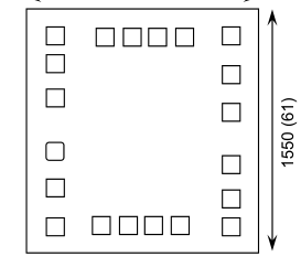
Die Dimensions in µm (mils)
1460 (57)
Mechanical Specification
| Die Size (Unsawn) | 1460 x 1550 57 x 61 | µm mils |
| Minimum Bond Pad Size | 108 x 108 4.25 x 4.25 | µm mils |
| Die Thickness | 350 (±20) 13.78 (±0.79) | µm mils |
| Top Metal Composition | Al 1%Si 1.1µm | |
| Back Metal Composition | N/A – Bare Si | |
Page 2

Rev 1.0
Pad Layout and Functions
10/03/21
| 18 17 16 15 14 13 19 12 20 11 1 10 2 DIE ID 9 3 4 5 6 7 7 | |
| 0,0 |
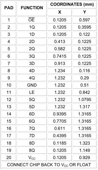
1460µm (57.48 mils)
Logic Diagram
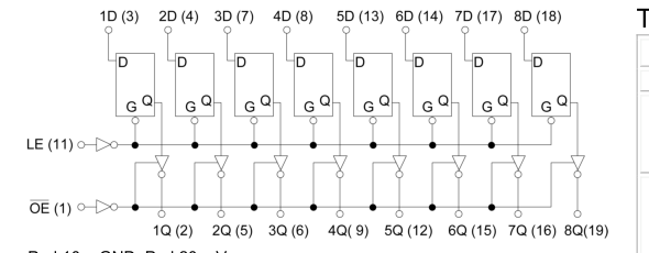
Truth Table
| INPUTS | OUTPUT | ||
| OE | LE | D | Q |
| L L L H | H H L X | H L X X | H L No Change Z |
| H = High level (steady state) L = Low level (steady state) Z = High Impedance X = Don’t care | |||
Pad 10 = GND, Pad 20 = VCC
Page 2 of 7
Page 3

Rev 1.0
Absolute Maximum Ratings1
10/03/21
| PARAMETER | SYMBOL | VALUE | UNIT |
|---|---|---|---|
| DC Supply Voltage (Referenced to GND) | V CC | -0.5 to +7.0 | V |
| DC Input Voltage (Referenced to GND) | V IN | -1.5 to V +1.5 CC | V |
| DC Output Voltage (Referenced to GND) | V OUT | -0.5 to V +0.5 CC | V |
| DC Input C urrent, per pad | I IN | ±20 | mA |
| DC Output Current, per pad | I OUT | ±35 | mA |
| DC Supply Current, V or GND CC | I CC | ±75 | mA |
| Power Dissipation in Still Air2 | P D | 750 | mW |
| Storage Temperature Range | T STG | -65 to 150 | °C |
- Operation above the absolute maximum rating may cause device failure. Operation at the absolute maximum ratings, for extended periods, may reduce device reliability. 2. Measured in plastic DIP package, results in die form are dependent on die attach and assembly method.
Recommended Operating Conditions3 (Voltages referenced to GND)
| PARAMETER | SYMBOL | MIN | MAX | UNITS | |
|---|---|---|---|---|---|
| Supply Voltage | V CC | 2 | 6 | V | |
| DC Input or Output Voltage | V ,V IN OUT | 0 | V CC | V | |
| Operating Temperature Range | T J | -55 | +125 | °C | |
| Input Rise or Fall Times | t, t r f | V = 2V CC | 0 | 1000 | ns |
| V = 4.5V CC | 0 | 500 | |||
| V = 6.0V CC | 0 | 400 | |||
- This device contains protection circuitry to guard against damage due to high static voltages or electric fields. However, precautions must be taken to avoid applications of any voltage higher than maximum rated voltages to this high-impedance circuit. For proper operation, VIN and VOUT should be constrained to the range GND ≤ (VIN or VOUT) ≤ VCC. Unused inputs must always be tied to an appropriate logic voltage level (e.g., either GND or VCC). Unused outputs must be left open.
DC Electrical Characteristics (Voltages Referenced to GND)
| PARAMETER | SYMBOL | V CC | CONDITIONS | LIMITS | UNITS | ||
|---|---|---|---|---|---|---|---|
| 25°C | 85°C | FULL RANGE4 | |||||
| Minimum H igh-Level Input Voltage | V IH | 2.0V | V = 0.1V or OUT V -0.1V CC │I │≤ 20µA OUT | 1.5 | 1.5 | 1.5 | V |
| 4.5V | 3.15 | 3.15 | 3.15 | ||||
| 6.0V | 4.2 | 4.2 | 4.2 | ||||
| Maximum Low-Level Input Voltage | V IL | 2.0V | V = 0.1V or OUT V -0.1V CC │I │≤ 20µA OUT | 0.5 | 0.5 | 0.5 | V |
| 4.5V | 1.35 | 1.35 | 1.35 | ||||
| 6.0V | 1.8 | 1.8 | 1.8 | ||||
| Minimum High-Level Output Vo ltage | V OH | 2V | V = V or V IN IH IL │I │≤ 20µA OUT | 1.9 | 1.9 | 1.9 | V |
| 4.5V | 4.4 | 4.4 | 4.4 | ||||
| 6.0V | 5.9 | 5.9 | 5.9 | ||||
| 4.5V | V = V or V IN IH IL │I │≤ 6.0mA OUT | 3.98 | 3.84 | 3.70 | V | ||
| 6.0V | V = V or V IN IH IL │I │≤ 7.8mA OUT | 5.48 | 5.34 | 5.20 | |||
- -55˚C ≤ TJ ≤ +125˚C
Page 3 of 7
Page 4

Rev 1.0
10/03/21
DC Electrical Characteristics Continued (Voltages referenced to GND)
| PARA METER | SYMBOL | V CC | CONDITIONS | LIMITS | UNITS | ||
|---|---|---|---|---|---|---|---|
| 25°C | 85°C | FULL RANGE4 | |||||
| Maximum Low-Level Output Voltage | V OL | 2V 4.5V 6.0V | V = V or V IN IH IL │I │≤ 20µA OUT | 0.1 | 0.1 | 0.1 | V |
| 0.1 | 0.1 | 0.1 | |||||
| 0.1 | 0.1 | 0.1 | |||||
| 4.5V | V = V or V IN IH IL │I │≤ 6.0mA OUT | 0.26 | 0.33 | 0.40 | V | ||
| 6.0V | V = V or V IN IH IL │I │≤ 7.8mA OUT | 0.26 | 0.33 | 0.40 | V | ||
| Maximum Input Leakage Current | I IN | 6.0V | V = V IN CC or GND | ±0.1 | ±1.0 | ±1.0 | µA |
| Maximum Quiescent Supply Current | I CC | 6.0V | V = V IN CC or GND, I = 0µA OUT | 4 | 40 | 160 | µA |
| Maximum Three-State Leakage Current | I OZ | 6.0V | Output in High- Impedance State, V = V or V IN IH IL, V = V or OUT CC GND | ±0.5 | ±5.0 | ±10.0 | µA |
AC Electrical Characteristics5
| PARAMETER | SYMBOL | V CC | CONDITIONS | LIMITS | UNITS | ||
|---|---|---|---|---|---|---|---|
| 25°C | 85°C | FULL RANGE4 | |||||
| Maxim um Propagation Delay, D to Q, (F igure 1,5) | t t PLH, PHL | 2.0V | C = 50pF, L Input t = t = 6ns r f | 125 | 155 | 190 | ns |
| 4.5V | 25 | 31 | 38 | ||||
| 6.0V | 21 | 26 | 32 | ||||
| Maxim um Propagation Delay, LE to Q, (Figure 2,5) | t t PLH, PHL | 2.0V | C = 50pF, L Input t = t = 6ns r f | 140 | 175 | 210 | ns |
| 4.5V | 28 | 35 | 42 | ||||
| 6.0V | 24 | 30 | 36 | ||||
| Maxim um Propagation Delay, OE to Q (Figure 3,6) | t t PLZ, PHZ | 2.0V | C = 50pF, L Input t = t = 6ns r f | 150 | 190 | 225 | ns |
| 4.5V | 30 | 38 | 45 | ||||
| 6.0V | 26 | 33 | 38 | ||||
| Maxim um Propagation Delay, OE to Q (Figure 3,6) | t t PZL, PZH | 2.0V | C = 50pF, L Input t = t = 6ns r f | 150 | 190 | 225 | ns |
| 4.5V | 30 | 38 | 45 | ||||
| 6.0V | 26 | 33 | 38 | ||||
5 Not production tested in die form, characterized by chip design
Page 4 of 7
Page 5

Rev 1.0
10/03/21
AC Electrical Characteristics continued5
| PARAMETER | SYMBOL | V CC | CONDITIONS | LIMITS | UNITS | ||
|---|---|---|---|---|---|---|---|
| 25°C | 85°C | FULL RANGE4 | |||||
| Maximum Output Transition Time, Any Output (Figure 1,5) | t t TLH, THL | 2.0V | C = 50pF, L Input t = t = 6ns r f | 60 | 75 | 90 | pF |
| 4.5V | 12 | 15 | 18 | ||||
| 6.0V | 10 | 13 | 15 | ||||
| Maximum Input Capacitance | C IN | - | C = 50pF, L Input t = t = 6ns r f | 10 | 10 | 10 | pF |
| Maximum 3-State Output Cap acitance | C OUT | - | C = 50pF, L Input t = t = 6ns r f High Z state | 15 | 15 | 15 | pF |
| Power Dissipation Capacitance (Per la tch)7 | C PD | 5V | - | TYPICAL | pF | ||
| 36 | |||||||
2f + ICC VCC.
- Used to determine the no-load dynamic power consumption: PD = CPD VCC
Timing Requirements6
| PARAMETER | SYMBOL | V CC | CONDITIONS | LIMITS | UNITS | ||
|---|---|---|---|---|---|---|---|
| 25°C | 85°C | FULL RANGE4 | |||||
| Minimum Setup Time, D to LE (Figure 4) | t SU | 2.0V | C = 50pF, L Input t = t = 6ns r f | 25 | 30 | 40 | ns |
| 4.5V | 5.0 | 6.0 | 8.0 | ||||
| 6.0V | 5.0 | 6.0 | 7.0 | ||||
| Minimum Hold Time, LE to D (Figure 4) | t h | 2.0V | C = 50pF, L Input t = t = 6ns r f | 5.0 | 5.0 | 5.0 | ns |
| 4.5V | 5.0 | 5.0 | 5.0 | ||||
| 6.0V | 5.0 | 5.0 | 5.0 | ||||
| Minimum Pulse Width, LE (Figure 4) | t w | 2.0V | C = 50pF, L Input t = t = 6ns r f | 60 | 75 | 90 | ns |
| 4.5V | 12 | 15 | 18 | ||||
| 6.0V | 10 | 13 | 15 | ||||
| Maximum Input Rise & Fall Times (Figure 4) | t, t r f | 2.0V | C = 50pF, L Input t = t = 6ns r f | 1000 | 1000 | 1000 | ns |
| 4.5V | 500 | 500 | 500 | ||||
| 6.0V | 400 | 400 | 400 | ||||
Page 5 of 7
Page 6

Switching Waveforms
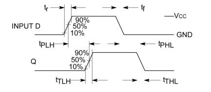
Figure 1 – Propagation Delay & Output Transition Time
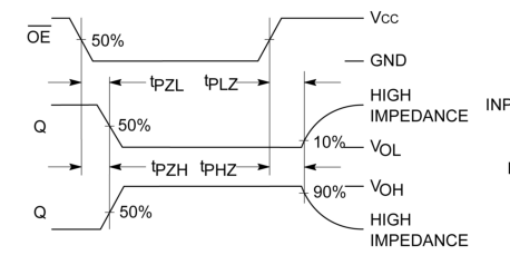
Figure 3 – Propagation Delay - Output Enable to Q
Page 6 of 7
Rev 1.0
10/03/21
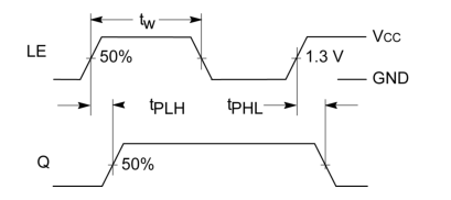
Figure 2 – Propagation Delay – Latch Enable to Q
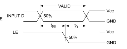
Figure 4 – Timing Requirements
Page 7

Rev 1.0
07/02/19
Test Circuits
TEST POINT
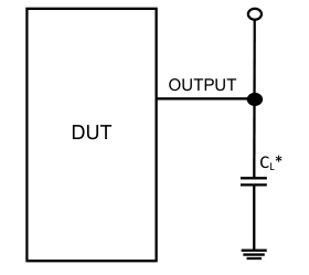
\* Includes all probe and jig capacitance
Figure 5
TEST POINT
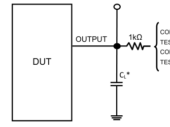
CONNECT TO VCC WHEN
TESTING tPLZ,& tPZL.
CONNECT TO GND WHEN
TESTING tPHZ,& tPZH
\* Includes all probe and jig capacitance
Figure 6
