
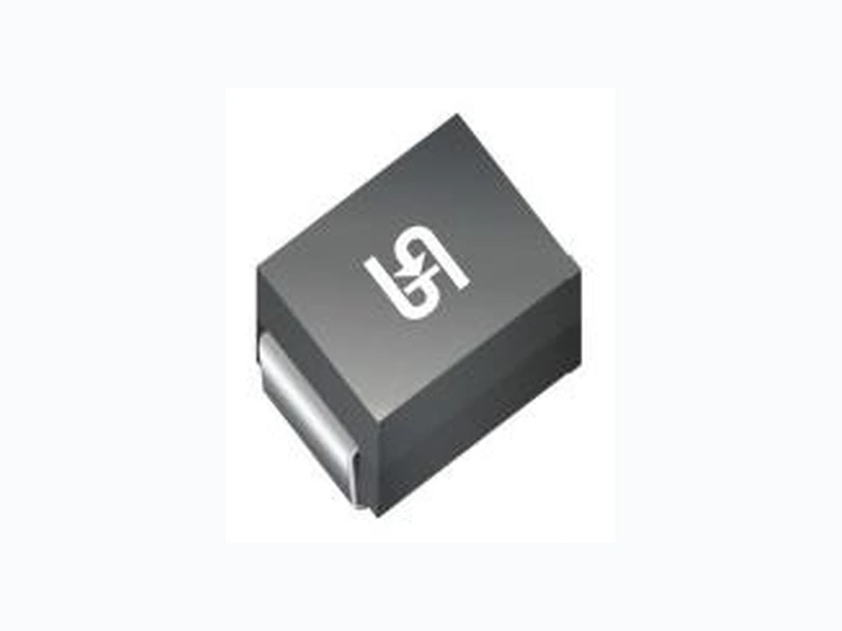
5.0SMDJ TSC
Document overview
- Manufacturer or author: Provided By digicamel.com
- PDF pages: 6
Technical content
5.0SMDJ16A - 5.0SMDJ100A Taiwan Semiconductor
1 Version:B1708
5000W, 16V - 100V Surface Mount Transient Voltage Suppressor
FEATURES
- 5000 watts peak pulse power capability at 10/1000μs waveform
- Ideal for automated placement
- Photo glass passivated junction
- Excellent clamping capability
- Fast response time: Typically less than 1.0ps
- Compliant to RoHS Directive 2011/65/EU and in accordance to WEEE 2002/96/EC
- Halogen-free according to IEC 61249-2-21
APPLICATIONS
- I/O interface
- AC/DC power supply
- Automotive MECHANICAL DATA
- Case: DO-214AB (SMC)
- Molding compound meets UL 94V-0 flammability rating
- Part no. with suffix "H" means AEC-Q101 qualified
- Packing code with suffix "G" means green compound (halogen-free)
- Moisture sensitivity level: level 1, per J-STD-020
- Terminal: Matte tin plated leads, solderable per J-STD-002
- Meet JESD 201 class 2 whisker test
- Polarity: As marked
- Weight: 0.30 g (approximately) KEY PARAMETERS PARAMETER VALUE UNIT VWM 16 - 100 V VBR (uni-directional) 17.8 - 123 V PPPSM 5000 W TJ MAX 175 °C Package DO-214AB (SMC) Configuration Stacked die DO-214AB (SMC) ABSOLUTE MAXIMUM RATINGS (TA = 25°C unless otherwise noted) PARAMETER SYMBOL VALUE UNIT Non-repetitive peak impulse power dissipation with 10/1000us waveform (1) PPPSM 5000 W Steady state power dissipation at TL=75°C (2) Ptot 6.25 W Forward Voltage @ IF=100A for Uni-directional only(3) VF 5 V Junction temperature TJ -55 to +175 °C Storage temperature TSTG -55 to +175 °C Notes: 1. Non-repetitive Current Pulse Per Fig. 3 and derated above TA=25°C Per Fig. 1 2. Units mounted on recommended PCB (16mm x 16mm Cu pad test board) 3. Pulse test with PW=0.3 ms THERMAL PERFORMANCE PARAMETER SYMBOL LIMIT UNIT Junction-to-lead thermal resistance per diode RӨJL 16 °C/W Junction-to-ambient thermal resistance per diode RӨJA 61 °C/W Junction-to-case thermal resistance per diode RӨJC 17 °C/W Thermal Performance Note: Units mounted on recommended PCB (16mm x 16mm Cu pad test board)
5.0SMDJ16A - 5.0SMDJ100A Taiwan Semiconductor
2 Version:B1708
ELECTRICAL SPECIFICATIONS (TA = 25°C unless otherwise noted) Part number Marking code Breakdown voltage VBR@IT (V) (Note 1) Test current IT (mA) Working stand- off voltage VWM (V) Maximum blocking leakage current IIB@VWM (µA) (Note 1) Maximum peak impulse current IPP (A) Maximum clamping voltage VC@IPP (V) Maximum Temp. coefficient of VBR αVBR@IT (mV/°C) Uni Uni Min. Max. 5.0SMDJ85A 5PGV 94.4 104 1 85 2 36.5 137 0.110 5.0SMDJ90A 5PGX 100 111 1 90 2 34.3 146 0.110 5.0SMDJ100A 5PGZ 111 123 1 100 2 30.9 162 0.110 Note: 1. Pulse test with PW=30 ms
5.0SMDJ16A - 5.0SMDJ100A Taiwan Semiconductor
3 Version:B1708
ORDERING INFORMATION
PART NO. PART NO. SUFFIX PACKING CODE PACKING CODE SUFFIX PACKAGE PACKING 5.0SMDJxxA (Note 1, 2) H G SMC 850 / 7" Plastic reel R6 3,000 / 13" Paper reel M6 3,000 / 13" Plastic reel Notes : 1. "xx" defines voltage from 16V (5.0SMDJ16A) to 100V (5.0SMDJ100A) 2. Whole series with green compound (halogen-free) EXAMPLE EXAMPLE P/N PART NO. PART NO. SUFFIX PACKING CODE PACKING CODE SUFFIX DESCRIPTION 5.0SMDJ16AHR7G 5.0SMDJ16A H R7 G AEC-Q101 qualified Green compound
5.0SMDJ16A - 5.0SMDJ100A Taiwan Semiconductor
4 Version:B1708
(TA = 25°C unless otherwise noted) Fig.1 Pulse Power or Current vs. Initial Junction Temperature Fig.2 Power Derating Curve Fig.3 Pulse Waveform Fig.4 Typical Junction Capacitance 100 0 25 50 75 100 125 150 175 TJ - INITAL TEMPERATURE (°C) 0.0 0.5 1.0 1.5 2.0 2.5 3.0 3.5 4.0 4.5 5.0 5.5 6.0 6.5 0 25 50 75 100 125 150 175 PD - POWER DISSIPATION (W) 100 1000 10000 0.1 1 10 100 REVERSE VOLTAGE (V) 100 120 140 0 0.5 1 1.5 2 2.5 3 IPPM, PEAK PULSE CURRENT (%) t, TIME (ms) td Peak value IPPM Rise time tr=10μs to 100% Half value-IPPM/2 10/1000μs, waveform as defined by R.E.A. Pulse width(td) is defined as the point where the peak current decays to 50% of IPPM CAPACITANCE (pF) 5.0SMDJ16A 5.0SMDJ51A 5.0SMDJ100A PEAK PULSE POWER (PPPM) OR CURRENT(IPP) DERATING IN PERCENTAGE, % LEAD TEMPERATURE (oC) Heat sink 16mm x 16mm Cu pad test board
5.0SMDJ16A - 5.0SMDJ100A Taiwan Semiconductor
5 Version:B1708
PACKAGE OUTLINE DIMENSIONS DO-214AB (SMC) DIM. Unit (mm) Unit (inch) Min Max Min Max A 2.90 3.20 0.114 0.126 B 6.60 7.11 0.260 0.280 C 5.59 6.22 0.220 0.245 D 2.00 2.62 0.079 0.103 E 1.00 1.60 0.039 0.063 F 7.75 8.13 0.305 0.320 G 0.10 0.20 0.004 0.008 H 0.15 0.31 0.006 0.012 SUGGESTED PAD LAYOUT MARKING DIAGRAM Symbol Unit (mm) Unit (inch) A 3.30 0.130 B 2.50 0.098 C 6.80 0.268 D 4.40 0.173 E 9.40 0.370 P/N = Marking Code G =Green compound YW = Date Code F = Factory Code
5.0SMDJ16A - 5.0SMDJ100A Taiwan Semiconductor
6 Version:B1708
Specifications of the products displayed herein are subject to change without notice. TSC or anyone on its behalf, assumes no responsibility or liability for any errors or inaccuracies. Information contained herein is intended to provide a product descrip tion only. No license, express or implied, to any intellectual property rights is granted by this document. Except as provided in TSC’s terms and conditions of sale for such products, TSC assumes no liability whatsoever, and disclaims any express or implie d warranty, relating to sale and/or use of TSC products including liability or warranties relating to fitness for a particular purpose, merchantability, or infringement of any patent, copyright, or other intellectual property right. The products shown her ein are not designed for use in medical, life -saving, or life -sustaining applications. Customers using or selling these products for use in such applications do so at their own risk and agree to fully indemnify TSC for any damages resulting from such improper use or sale.