
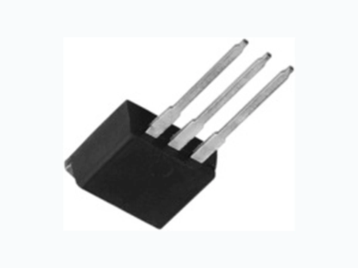
32CTQ030S VISHAY
Document overview
- Manufacturer or author: Provided By www.digicamel.com(free datasheet download site)
- PDF pages: 6
Technical content
Document Number: 93961 For technical ques tions, contact: diodes-tech@vishay.com www.vishay.com Revision: 21-Aug-08 1 Schottky Rectifier, 2 x 15 A Vishay High Power Products
FEATURES
- 150 °C TJ operation Low forward voltage drop High frequency operation High purity, high temperature epoxy encapsulation for enhanced mechanical strength and moisture resistance Guard ring for enhanced ruggedness and long term reliability Designed and qualified for Q101 level
DESCRIPTION
The 32CTQ... Schottky rectifie r series has been optimized for low reverse leakage at high temperature. The proprietary barrier technology allows for reliable operation up to 150 °C junction temperature. Typical applications are in switching power supplies, converters, freewheeling diodes, and reverse battery protection. PRODUCT SUMMARY IF(AV) 2 x 15 A VR 25/30 V 32CTQ...S Base common cathode D2PAK TO-262 32CTQ...-1 Anode Anode Common cathode 1 3 Base common cathode Anode Anode Common cathode 1 3 MAJOR RATINGS AND CHARACTERISTICS SYMBOL CHARACTERISTICS VALUES UNITS IF(AV) Rectangular waveform 30 A VRRM 25/30 V IFSM tp = 5 µs sine 900 A VF 15 Apk, TJ = 125 °C 0.40 V TJ Range - 55 to 150 °C VOLTAGE RATINGS PARAMETER SYMBOL 32CTQ025S 32CTQ025-1 32CTQ030S 32CTQ030-1 UNITS Maximum DC reverse voltage V R 25 30 V Maximum working peak reverse voltage V RWM ABSOLUTE MAXIMUM RATINGS PARAMETER SYMBOL TEST CONDITIONS VALUES UNITS Maximum average forward current See fig. 5 IF(AV) 50 % duty cycle at TC = 115 °C, rectangular waveform 30 AMaximum peak one cycle non-repetitive surge current See fig. 7 IFSM 5 µs sine or 3 µs rect. pulse Following any rated load condition and with rated VRRM applied 900 10 ms sine or 6 ms rect. pulse 250 Non-repetitive avalanche energy E AS TJ = 25 °C, IAS = 1.20 A, L = 11.10 mH 13 mJ Repetitive avalanche current I AR Current decaying linearly to zero in 1 µs Frequency limited by TJ maximum VA = 1.5 x VR typical 3A
www.vishay.com For technical questi ons, contact: diodes-tech@vishay.com Document Number: 93961
2 Revision: 21-Aug-08
Vishay High Power Products Schottky Rectifier, 2 x 15 A Note (1) Pulse width < 300 µs, duty cycle < 2 % ELECTRICAL SPECIFICATIONS PARAMETER SYMBOL TEST CONDITIONS VALUES UNITS Maximum forward voltage drop See fig. 1 VFM (1) 15 A TJ = 25 °C 0.49 V 30 A 0.58 15 A TJ = 125 °C 0.40 30 A 0.53 Maximum reverse leakage current See fig. 2 IRM (1) TJ = 25 °C VR = Rated VR 1.75 mA TJ = 125 °C 97 Threshold voltage V F(TO) TJ = TJ maximum 0.233 V Forward slope resistance r t 9.09 m Ω Maximum junction capacitance per leg C T VR = 5 VDC (test signal range 100 kHz to 1 MHz) 25 °C 1300 pF Typical series inductance per leg L S Measured lead to lead 5 mm from package body 8.0 nH Maximum voltage rate of change dV/dt Rated V R 10 000 V/µs THERMAL - MECHANICAL SPECIFICATIONS PARAMETER SYMBOL TEST CONDITIONS VALUES UNITS Maximum junction and storage temperature range TJ, TStg - 55 to 150 °C Maximum thermal resistance, junction to case per leg RthJC DC operation See fig. 4 3.25 °C/WTypical thermal resistance, case to heatsink RthCS Mounting surface, smooth and greased 0.50 Approximate weight 0.07 oz. Mounting torque minimum 6 (5) kgf ⋅ cm (lbf ⋅ in)maximum 12 (10) Marking device Case style D2PAK 32CTQ025S 32CTQ030S Case style TO-262 32CTQ025-1 32CTQ030-1
Document Number: 93961 For technical ques tions, contact: diodes-tech@vishay.com www.vishay.com Revision: 21-Aug-08 3 Schottky Rectifier, 2 x 15 A Vishay High Power Products Fig. 1 - Maximum Forward Voltage Drop Characteristics Fig. 2 - Typical Values of Reverse Current vs. Reverse Voltage Fig. 3 - Typical Junction Capacitance vs. Reverse Voltage Fig. 4 - Maximum Thermal Impedance ZthJC Characteristics 100 1000 IF - Instantaneous Forward Current (A) VFM - Forward Voltage Drop (V) TJ = 150 °C TJ = 125 °C TJ = 25 °C 0.001 100 0.1 0.01 1000 IR - Reverse Current (mA) VR - Reverse Voltage (V) 1051 5 2 0 30250 TJ = 150 °C TJ = 125 °C TJ = 100 °C TJ = 75 °C TJ = 50 °C TJ = 25 °C 100 1000 10 000 CT - Junction Capacitance (pF) VR - Reverse Voltage (V) 105 1 52 02 5 35300 TJ = 25 °C 0.001 0.01 0.1 t1 - Rectangular Pulse Duration (s) ZthJC - Thermal Impedance (°C/W) Single pulse (thermal resistance) D = 0.75 D = 0.50 D = 0.33 D = 0.25 D = 0.20 PDM Notes: 1. Duty factor D = t1/t2 2. Peak TJ = PDM x ZthJC + TC
www.vishay.com For technical questi ons, contact: diodes-tech@vishay.com Document Number: 93961
4 Revision: 21-Aug-08
Vishay High Power Products Schottky Rectifier, 2 x 15 A Fig. 5 - Maximum Allowable Case Temperature vs. Average Forward Current Fig. 6 - Forward Power Loss Characteristics Fig. 7 - Maximum Non-Repetitive Surge Current Fig. 8 - Unclamped Inductive Test Circuit Note (1) Formula used: TC = TJ - (Pd + PdREV) x RthJC; Pd = Forward power loss = IF(AV) x VFM at (IF(AV)/D) (see fig. 6); PdREV = Inverse power loss = VR1 x IR (1 - D); IR at VR1 = 80 % rated VR 100 110 120 130 140 160 150 Allowable Case Temperature (°C) IF(AV) - Average Forward Current (A) 1051 5 2 0 250 DC See note (1) Square wave (D = 0.50) 80 % rated VR applied Average Power Loss (W) IF(AV) - Average Forward Current (A) 1051 5 2 0 250 DC RMS limit D = 0.20 D = 0.25 D = 0.33 D = 0.50 D = 0.75 100 1000 IFSM - Non-Repetitive Surge Current (A) tp - Square Wave Pulse Duration (µs) 100 1000 10 00010 At any rated load condition and with rated VRRM applied following surge Current monitor High-speed switchD.U.T. Rg = 25 Ω + Freewheel diode Vd = 25 V L IRFP460 40HFL40S02
Document Number: 93961 For technical ques tions, contact: diodes-tech@vishay.com www.vishay.com Revision: 21-Aug-08 5 Schottky Rectifier, 2 x 15 A Vishay High Power Products ORDERING INFORMATION TABLE - Current rating (30 A) - Circuit configuration: C = Common cathode - T = TO-220 - Schottky “Q” series - Voltage rating S = D2PAK -1 = TO-262 None = Tube (50 pieces) TRL = Tape and reel (left oriented - for D2PAK only) TRR = Tape and reel (right oriented - for D2PAK only) None = Standard production PbF = Lead (Pb)-free Device code 513 24 678
32 C T Q 030 S TRL -
025 = 25 V 030 = 30 V LINKS TO RELATED DOCUMENTS Dimensions http://www.vishay.com/doc?95014 Part marking information http://www.vishay.com/doc?95008 Packaging information http://www.vishay.com/doc?95032
Document Number: 91000 www.vishay.com Revision: 18-Jul-08 1 Disclaimer Legal Disclaimer Notice Vishay All product specifications and data are subject to change without notice. Vishay Intertechnology, Inc., its affiliates, agents, and employees, and all persons acting on its or their behalf (collectively, “Vishay”), disclaim any and all liability for any errors, inaccuracies or incompleteness contained herein or in any other disclosure relating to any product. Vishay disclaims any and all li ability arising out of the use or application of any product described herein or of any information provided herein to the maximum extent permit ted by law. The product specifications do not expand or otherwise modify Vishay’s terms and conditions of purcha se, including but not limited to the warranty expressed therein, which apply to these products. No license, express or implied, by estoppel or otherwise, to any intellectual property rights is granted by this document or by any conduct of Vishay. The products shown herein are not designed for use in medi cal, life-saving, or life-sustaining applications unless otherwise expressly indicated. Customers using or selling Vishay products not expressly indicated for use in such applications do so entirely at their own risk and agree to fully indemnify Vishay for any damages arising or resulting from such use or sale. Please contact authorized Vishay personnel to obtain written terms and conditions regarding products designed for such applications. Product names and markings noted herein may be trademarks of their respective owners.