

 Download PDF
DATASHEET SEARCH SITE
Document overview
- PDF pages: 13
Technical content
Page 1
DATA SHEET
POWER SUPPLY 14D series
RoHS compliant & Halogen free
Page 2

Metal Oxide Varistor (MOV) Data Sheet
Features
■ Wide operating voltage (V1mA) range from 18V to 1800V ■ Fast responding to transient over-voltage ■ Large absorbing transient energy capability ■ Low clamping ratio and no follow-on current ■ Meets MSL level 1, per J-STD-020 ■ Operating Temperature:-40℃ ~ +105℃ ■ Storage Temperature:-40℃ ~ +125℃ ■ Safety certification: UL: E327997 CSA: 246579 VDE: 40027827
Applications
■ Transistor, diode, IC, thyristor or triac semiconductor protection ■ Surge protection in consumer electronics ■ Surge protection in industrial electronics ■ Surge protection in electronic home appliances, gas and petroleum appliances ■ Relay and electromagnetic valve surge absorption
Part Number Code
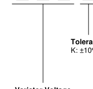
Tolerance
Type D: Disk
Surge Series
Varistor Voltage
No suffix: Standard type
180: 18V
J: High Surge type
101: 100V 102: 1000V
Element Diameter 14=14mm
Packing No suffix: Bulk
Pitch
TB: Tape & Box
No suffix: 7.5mm TR: Tape & Reel P10: 10mm
Lead Shape No suffix: Straight leads O: Outside crimped leads F: Y Kinked leads
Page 3

Dimensions
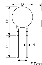
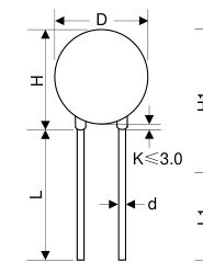
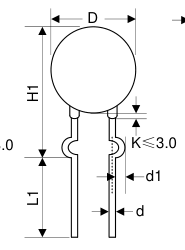
T
T
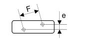
O Type
| Table 2 Unit: mm | |||||
|---|---|---|---|---|---|
| Model | T | e | Model | T | e |
| 180K | 2.0~3.9 | 1.5 | 361K | 2.9~5.2 | 2.7 |
| 220K | 2.1~4.0 | 1.6 | 391K | 3.0~5.4 | 2.8 |
| 270K | 2.1~4.1 | 1.8 | 431K | 3.2~5.6 | 3.0 |
| 330K | 2.2~4.3 | 1.7 | 471K | 3.3~5.8 | 3.2 |
| 390K | 2.1~4.1 | 1.8 | 511K | 3.4~6.1 | 3.4 |
| 470K | 2.2~4.3 | 1.9 | 561K | 3.6~6.4 | 3.6 |
| 560K | 2.3~4.6 | 2.1 | 621K | 3.8~6.8 | 3.9 |
| 680K | 2.4~4.8 | 2.4 | 681K | 4.0~7.1 | 4.2 |
| 820K | 2.1~4.1 | 1.8 | 751K | 4.3~7.2 | 4.3 |
| 101K | 2.4~4.2 | 2.0 | 781K | 4.4~7.3 | 4.4 |
| 121K | 2.4~4.4 | 2.2 | 821K | 4.6~7.5 | 4.6 |
| 151K | 2.2~4.1 | 1.8 | 911K | 4.8~7.5 | 5.0 |
| 181K | 2.3~4.2 | 1.9 | 102K | 5.4~8.0 | 5.0 |
| 201K | 2.4~4.3 | 2.0 | 112K | 5.8~8.5 | 5.4 |
| 221K | 2.5~4.4 | 2.1 | 122K | 5.9~9.0 | 5.8 |
| 241K | 2.6~4.5 | 2.2 | 142K | 6.9~10.5 | 6.6 |
| 271K | 2.6~4.6 | 2.4 | 162K | 7.4~11.0 | 7.4 |
| 301K | 2.7~4.6 | 2.5 | 182K | 7.6~12.0 | 8.2 |
| 331K | 2.7~5.0 | 2.5 | |||
| Table 1 Unit: mm | |
|---|---|
| Symbol | Dimension |
| H | 14.5~20.0 |
| H1 | 17.0~21.0 |
| L(min.) | 20.0 |
| L1(min.) | 15.0 |
| D | 14.0~16.5 |
| F | 7.5±0.8/10.0±1.0 |
| T | Table 2 |
| e(±0.8) | Table 2 |
| d(±0.05) | 0.8 |
| d1(±0.4) | 1.4 |
Page 4

Electrical Characteristics
| Part Numbe r | Maximum Allowable Voltage | Varistor Voltage | Maximum Clamping Voltage | Withstanding Surge Current | Maximum Energy (10/1000μs) | Rated Power | Typical Capacitance (Reference) | |||||
|---|---|---|---|---|---|---|---|---|---|---|---|---|
| Standard | High Surge | V (V) AC | V (V) DC | V (V) 1mA | I (A) P | V (V) C | I (A) Standard | I (A) High Surge | (J) Standard | (J) High Surge | (W) | @1KHz (pf) |
| 180KD14 | 180KD14J | 11 | 14 | 18(15~21.6) | 10 | 36 | 1000 | 2000 | 4.0 | 7.0 | 0.1 | 11100 |
| 220KD14 | 220KD14J | 14 | 18 | 22(19.5~26) | 10 | 43 | 1000 | 2000 | 5.0 | 8.0 | 0.1 | 9100 |
| 270KD14 | 270KD14J | 17 | 22 | 27(24~31) | 10 | 53 | 1000 | 2000 | 6.0 | 10.0 | 0.1 | 7400 |
| 330KD14 | 330KD14J | 20 | 26 | 33(29.5~36.5) | 10 | 65 | 1000 | 2000 | 7.5 | 12.0 | 0.1 | 6100 |
| 390KD14 | 390KD14J | 25 | 31 | 39(35~43) | 10 | 77 | 1000 | 2000 | 8.6 | 13.0 | 0.1 | 5100 |
| 470KD14 | 470KD14J | 30 | 38 | 47(42~52) | 10 | 93 | 1000 | 2000 | 10.0 | 17.0 | 0.1 | 4300 |
| 560KD14 | 560KD14J | 35 | 45 | 56(50~62) | 10 | 110 | 1000 | 2000 | 11.0 | 20.0 | 0.1 | 3600 |
| 680KD14 | 680KD14J | 40 | 56 | 68(61~75) | 10 | 135 | 1000 | 2000 | 14.0 | 24.0 | 0.1 | 2900 |
| 820KD14 | 820KD14J | 50 | 65 | 82(74~90) | 50 | 135 | 4500 | 6000 | 22.0 | 27.0 | 0.6 | 2400 |
| 101KD14 | 101KD14J | 60 | 85 | 100(90~110) | 50 | 165 | 4500 | 6000 | 28.0 | 33.0 | 0.6 | 2000 |
| 121KD14 | 121KD14J | 75 | 100 | 120(108~132) | 50 | 200 | 4500 | 6000 | 32.0 | 40.0 | 0.6 | 1700 |
| 151KD14 | 151KD14J | 95 | 125 | 150(135~165) | 50 | 250 | 4500 | 6000 | 40.0 | 53.0 | 0.6 | 1300 |
| 181KD14 | 181KD14J | 115 | 150 | 180(162~198) | 50 | 300 | 4500 | 6000 | 50.0 | 60.0 | 0.6 | 1100 |
| 201KD14 | 201KD14J | 130 | 170 | 200(180~220) | 50 | 340 | 4500 | 6000 | 57.0 | 70.0 | 0.6 | 1000 |
| 221KD14 | 221KD14J | 140 | 180 | 220(198~242) | 50 | 360 | 4500 | 6000 | 60.0 | 78.0 | 0.6 | 900 |
| 241KD14 | 241KD14J | 150 | 200 | 240(216~264) | 50 | 395 | 4500 | 6000 | 63.0 | 84.0 | 0.6 | 830 |
| 271KD14 | 271KD14J | 175 | 225 | 270(243~297) | 50 | 455 | 4500 | 6000 | 70.0 | 99.0 | 0.6 | 740 |
| 301KD14 | 301KD14J | 190 | 250 | 300(270~330) | 50 | 500 | 4500 | 6000 | 77.0 | 108 | 0.6 | 670 |
| 331KD14 | 331KD14J | 210 | 275 | 330(297~363) | 50 | 550 | 4500 | 6000 | 85.0 | 115 | 0.6 | 610 |
| 361KD14 | 361KD14J | 230 | 300 | 360(324~396) | 50 | 595 | 4500 | 6000 | 93.0 | 130 | 0.6 | 560 |
| 391KD14 | 391KD14J | 250 | 320 | 390(351~429) | 50 | 650 | 4500 | 6000 | 100 | 140 | 0.6 | 510 |
| 431KD14 | 431KD14J | 275 | 350 | 430(387~473) | 50 | 710 | 4500 | 6000 | 115 | 155 | 0.6 | 460 |
| 471KD14 | 471KD14J | 300 | 385 | 470(423~517) | 50 | 775 | 4500 | 6000 | 118 | 175 | 0.6 | 430 |
| 511KD14 | 511KD14J | 320 | 415 | 510(459~561) | 50 | 845 | 4500 | 6000 | 121 | 180 | 0.6 | 390 |
| 561KD14 | 561KD14J | 350 | 460 | 560(504~616) | 50 | 925 | 4500 | 6000 | 125 | 185 | 0.6 | 360 |
| 621KD14 | 621KD14J | 385 | 505 | 620(558~682) | 50 | 1025 | 4500 | 6000 | 128 | 190 | 0.6 | 320 |
| 681KD14 | 681KD14J | 420 | 560 | 680(612~748) | 50 | 1120 | 4500 | 6000 | 130 | 200 | 0.6 | 290 |
| 751KD14 | 751KD14J | 460 | 615 | 750(675~825) | 50 | 1240 | 4500 | 6000 | 143 | 210 | 0.6 | 270 |
| 781KD14 | 781KD14J | 485 | 640 | 780(702~858) | 50 | 1290 | 4500 | 6000 | 148 | 220 | 0.6 | 260 |
| 821KD14 | 821KD14J | 510 | 670 | 820(738~902) | 50 | 1355 | 4500 | 6000 | 157 | 235 | 0.6 | 240 |
| 911KD14 | 911KD14J | 550 | 745 | 910(819~1001) | 50 | 1500 | 4500 | 6000 | 175 | 255 | 0.6 | 220 |
| 102KD14 | 102KD14J | 625 | 825 | 1000(900~1100) | 50 | 1650 | 4500 | 6000 | 190 | 280 | 0.6 | 200 |
| 112KD14 | 112KD14J | 680 | 895 | 1100(990~1210) | 50 | 1815 | 4500 | 6000 | 213 | 310 | 0.6 | 180 |
| 122KD14 | 122KD14J | 750 | 990 | 1200(1080~1320) | 50 | 1980 | 4500 | 6000 | 232 | 324 | 0.6 | 160 |
| 142KD14 | 142KD14J | 880 | 1140 | 1400(1260~1540) | 50 | 2310 | 4500 | 6000 | 238 | 327 | 0.6 | 150 |
| 162KD14 | 162KD14J | 1000 | 1280 | 1600(1440~1760) | 50 | 2640 | 4500 | 6000 | 243 | 331 | 0.6 | 140 |
| 182KD14 | 182KD14J | 1100 | 1465 | 1800(1620~1980) | 50 | 2970 | 4500 | 5000 | 250 | 335 | 0.6 | 130 |
Notes: 1. The tolerance of varistor voltage between 18V and 27V is more than 10%. 2. Varistor voltage≥1200V, structure diagram is F type. 3. Leakage Current (@83% of V1mA):IR≤50μA (180K~680K) ; IR≤25μA (820K~182K)
Page 5

Electrical Ratings
| Ite ms | Test Condition/Description | Requirement |
|---|---|---|
| Varistor Voltage | The voltage between two terminals with the specified measuring current 1mA.DC applied is called Vb. | To meet the Specified value |
| Maximum Allowable Voltage | The recommended maximum sine wave voltage (RMS) or the Maximum DC voltage can be applied continuously. | |
| Maximum Clamping Voltage | The maximum voltage between two terminals with the specification standard impulse current. Applied waveform: 8/20μs Crest value 100 90 (%) Current 50 20µs 10 8µs 0 Time Impulse Width | |
| Rated Wattage | The maximum average power that can be applied within the specified ambient temperature. | |
| Energy | The maximum energy within the varistor voltage change of ±10% when one impulse of 10/1000μs or 2ms is applied. | |
| Withstanding Surge Current | The maximum current within the varistor voltage change of ±10% with the standard impulse current (8/20μs) applied one time. | |
| Varistor Voltage Temp. Coefficient | V 1mA@85℃-V 1mA@25℃ × 1 × 100%(%/℃) V 60 1mA@25℃ | ≤0.05%/℃ |
| V 1mA@-40℃-V 1mA@25℃ × 1 × 100%(%/℃) V 65 1mA@25℃ | ||
| Surge Life | The change of Vb shall be measured after the impulse listed below which is applied 10,000 times continuously with the interval of ten seconds at room temperature. 180K to 680K 75A (8/20μs) 14Φ series 820K to 182K 150A (8/20μs) |
| 14Φ series | 180K to 680K | 75A (8/20μs) |
| 820K to 182K | 150A (8/20μs) |
Page 6

Soldering Recommendation
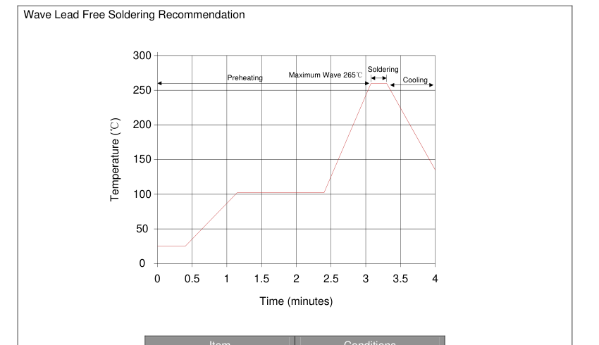
| Item | Conditions |
|---|---|
| Peak Temperature | 265℃ |
| Dipping Time | 10 seconds (max.) |
| Soldering | 1 time |

| Item | Conditions |
|---|---|
| Temperature of Soldering Iron-tip | 360℃ (max.) |
| Soldering Time | 3 seconds (max.) |
| Distance from Varistor | 2mm (min.) |
Page 7

Mechanical Characteristics
| Ite ms | Test conditions / Methods | Specifications |
|---|---|---|
| Tensile Strength of Ter minals | Gradually applying the force specified and keeping the unit fixed for 10±1 sec. Terminal diameter (mm) Force (kg) 0.5<d≤0.8 1.0 0.8<d≤1.25 2.0 1.25<d 4.0 | No visible damage | V /V |≤5% 1mA 1mA |
| Bending Strength of Terminals | Hold specimen and apply the force specified below to each lead. Bend the specimen to 90°, then return to the original position. Repeat the procedure in the opposite direction. Terminal diameter (mm) Force (kg) 0.5<d≤0.8 0.5 0.8<d≤1.25 1.0 1.25<d 2.0 | No visible damage | V /V |≤5% 1mA 1mA |
| Vibration | Frequency range: 10~55 Hz Amplitude: 0.75mm or 98m/s2 Direction: 3 mutually perpendicular directions, 2hrs each. | No visible damage | V /V |≤5% 1mA 1mA |
| Solder ability | Solder Temp: 245±5℃ Dipping Time: 2±0.5 sec | At least 95% of terminal electrode is covered by new solder |
| Resistance to Soldering Heat | Solder Temp: 260±5℃ Dipping Time: 10±1 sec | No visible damage | V /V |≤10% 1mA 1mA |
Reliability
| Items | Test conditions / Methods | Specifications |
|---|---|---|
| High Temperature Storage | Ambient Temp: 125±2℃ Duration: 1000hrs | | V /V |≤5% 1mA 1mA |
| Low Temperature Storage | Ambient Temp: -40±2℃ Duration: 1000hrs | | V /V |≤5% 1mA 1mA |
| Humidity | Ambient Temp: 40±2℃, 90~95% R.H. Duration: 1000hrs | | V /V |≤5% 1mA 1mA |
| Temperature Cycle | The conditions shown below shall be repeated 5 cycles Step Temperature (℃) Period (minutes) 1 -40±3 30±3 2 Room temperature 15±3 3 125±3 30±3 4 Room temperature 15±3 | No visible damage | V /V |≤5% 1mA 1mA |
| High Temperature Load | Ambient Temp: 105±2℃ Duration: 1000hrs Load: Max. Allowable Voltage In AC eara. | | V /V |≤10% 1mA 1mA |
| Damp Heat Load | Ambient Temp: 40±2℃, 90~95% R.H. Duration: 1000hrs Load: Max. Allowable Voltage | No visible damage | V /V |≤10% 1mA 1mA |
| Voltage Proof | Metal balls method, 2500Vac 1 min. | No visible damage |
| Step | Temperature (℃) | Period (minutes) |
|---|---|---|
| 1 | -40±3 | 30±3 |
| 2 | Room temperature | 15±3 |
| 3 | 125±3 | 30±3 |
| 4 | Room temperature | 15±3 |
Page 8

Maximum Surge Current Derating Curve
| 180KD14 to 680KD14 10000 1000 1 2 (A) 10 102 Current 100 103 104 105 106 Surge 10 Max. 1 0.1 10 100 1000 10000 Td (μs) | 820KD14 to 182KD14 10000 1 2 1000 10 102 (A) 103 104 Current 100 105 106 Surge 10 Max. 1 0.1 10 100 1000 10000 Td (μs) |
|---|---|
| 180KD14J to 680KD14J 10000 1 1000 2 10 102 (A) 103 Current 100 104 105 106 Surge 10 Max. 1 0.1 10 100 1000 10000 Td (μs) | 820KD14J to 182KD14J 10000 1 2 10 1000 102 103 (A) 104 Current 105 100 106 Surge 10 Max. 1 0.1 10 100 1000 10000 Td (μs) |
Page 9

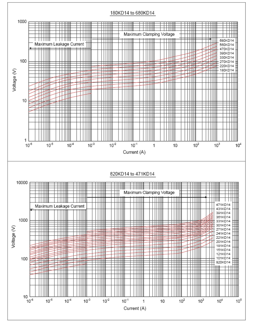
Maximum Leakage Current and Maximum Clamping Voltage Curve
Page 10

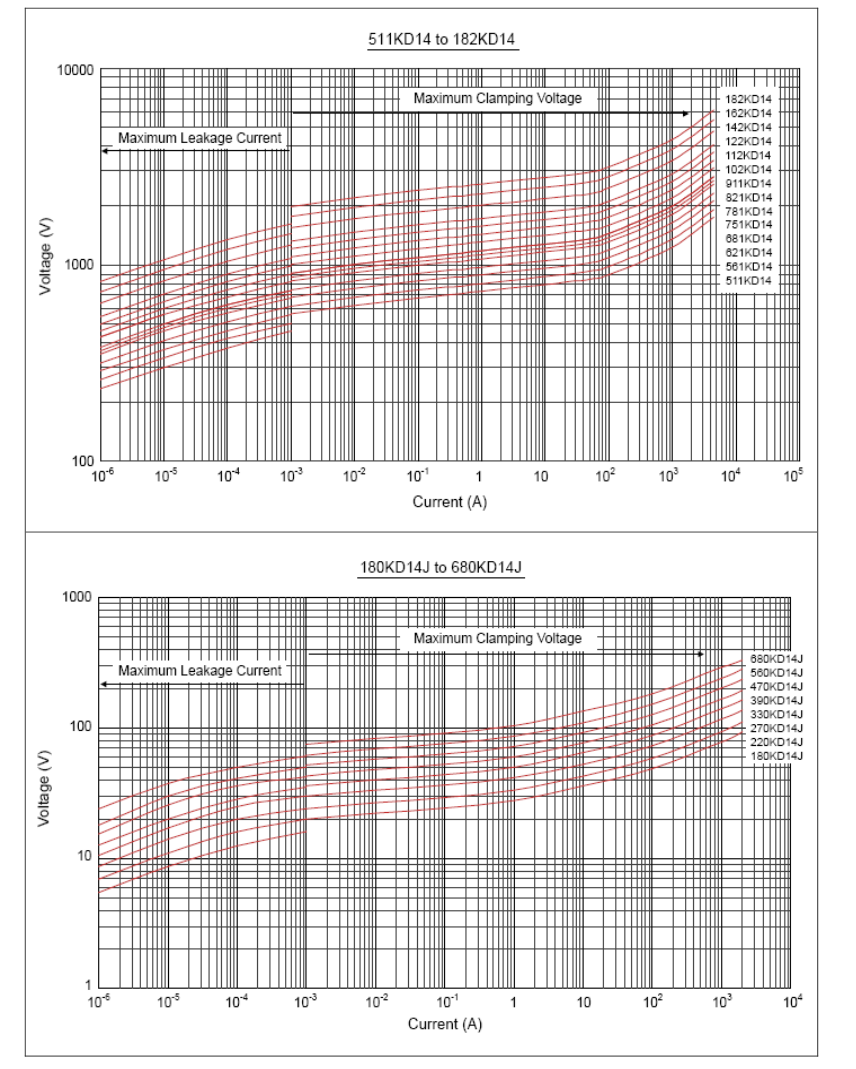
Maximum Leakage Current and Maximum Clamping Voltage Curve
Page 11

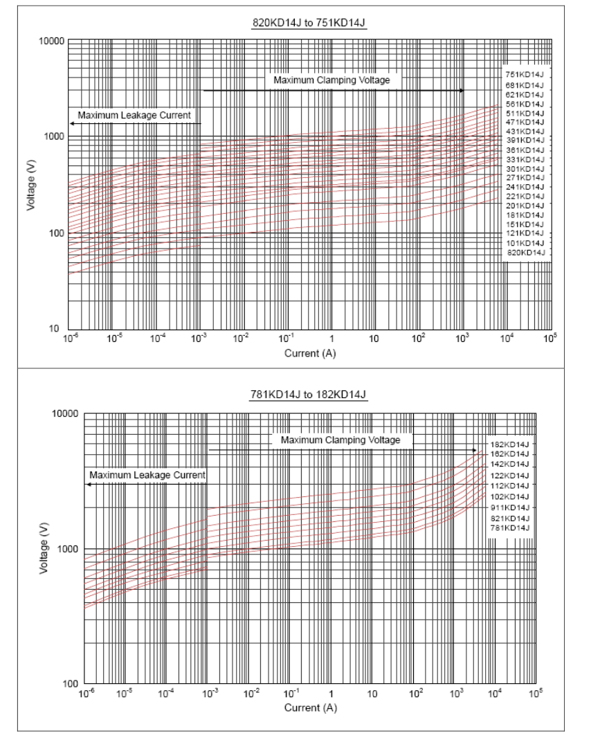
Maximum Leakage Current and Maximum Clamping Voltage Curve
Page 12

Marking Code
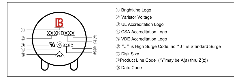
Taping Dimensions
| P2 P h B W2 H W0 W D0 P1 P0 F W1 t | Symbol | Dimensions (mm) |
| P | 25.4±1.0 | |
| P0 | 12.7±1.0 | |
| P1 | 8.95±0.7 | |
| P2 | 12.7±1.3 | |
| F | 7.5±0.8 | |
| h | 0±4 | |
| W | 18.0±1.0 | |
| W0 | 12.0±1.0 | |
| W1 | 9.0±0.5 | |
| W2 | 3.0max | |
| H | 20.0±2.0 | |
| D0 | 4.0±0.2 | |
| t | 0.6±0.3 | |
| B | 40max |
Page 13

Quantity
| Packaging Dimensions (Unit: mm) | Quantity |
|---|---|
| Exposure in bulk Max. 125 Max. 165 250 Max. | 400pcs/bag 4bags/box (180K~331K) |
| 300pcs/bag 4bags/box (361K~621K) | |
| 250pcs/bag 4bags/box (681K~112K) | |
| 150pcs/bag 4bags/box (122K~182K) | |
| Cut the feet in bulk ax. M 65 Max. 185 245 Max. | 400pcs/bag 4bags/box (180K~331K) |
| 300pcs/bag 4bags/box (361K~621K) | |
| 250pcs/bag 4bags/box (681K~112K) | |
| 150pcs/bag 4bags/box (122K~182K) | |
| Tape & Box ax. M 60 Max. 250 340 Max. | 750pcs/box (180K~331K) |
| 500pcs/box (361K~621K) | |
| 400pcs/box (681K~751K) | |
| Tape & Reel Max. 60 Max. 365 365 Max. 55 Max. 30±1 Φ365 Max. | 1000pcs/reel (180K~331K) |
| 750pcs/reel (361K~621K) | |
| 500pcs/reel (681K~751K) |