
DATASHEET SEARCH SITE
Document overview
- Manufacturer or author: Provided By digicamel.com
- PDF pages: 5
Technical content
Features
- For surface mounted applications in order to optimize board space
- Low profile package
- Typical failure mode is short from over-specified voltage or current
- Whisker test is conducted based on JEDEC JESD201A per its table 4a and 4c
- IEC-61000-4-2 ESD 30kV(Air), 30kV (Contact)
- I PP is specified @ 8/20µS surge waveform
- Built-in strain relief
- VBR @ TJ= VBR@25°C x (1+αT x (TJ - 25)) (αT :Temperature Coefficient, typical value is 0.1%)
- Glass passivated chip junction
- Fast response time: typically less than 1 .0ps from 0V to BV min
- Excellent clamping capability
- Low incremental surge resistance
- High temperature to reflow soldering guaranteed: 260°C/40sec
- Meet MSL level1, per J-STD-020, LF maximun peak of 260
- Matte tin lead–free plated
- Halogen free and RoHS compliant
- Pb-free E3 means 2nd level interconnect is Pb-free and the terminal finish material is tin(Sn) (IPC/JEDEC J-STD- 609A.01) 3.0SMC Series Functional Diagram Bi-directional Uni-directional Cathode Anode Uni-directional RoHS Pb e3 Datasheet Additional Infomarion Resources Samples
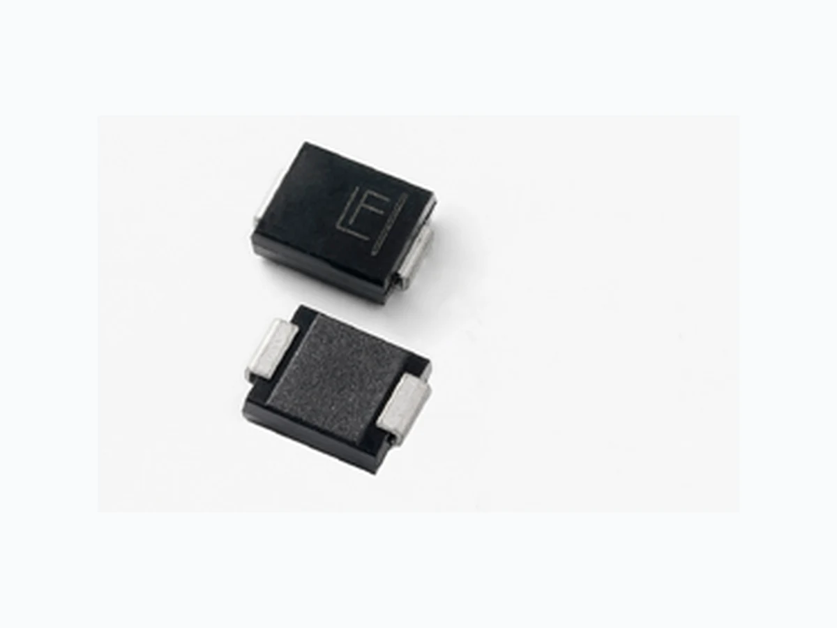
T ransient Voltage Suppression Diodes © 2015 Littelfuse, Inc. Specifications are subject to change without notice. Revised: 11/20/15 Surface Mount > 3.0SMC series TVS Diode Arrays (SPA™ Family of Products) Physical Specifications Weight 0.007 ounce, 0.21 grams Case JEDEC DO214AB. Molded plastic body over glass passivated junction Polarity Color band denotes positive end (cathode) except Bidirectional. T erminal Matte Tin-plated leads, Solderable per JESD22-B102 Dimensions Dimensions Inches Millimeters Min Max Min Max A 0.114 0.126 2.900 3.200 B 0.260 0.280 6.600 7. 11 0 C 0.220 0.245 5.590 6.220 D 0.079 0.103 2.060 2.620 E 0.030 0.060 0.760 1 .520 F - 0.008 - 0.203 G 0.305 0.320 7 .750 8.130 H 0.006 0.012 0.152 0.305 I 0.129 - 3.300 - J 0.094 - 2.400 - K - 0.165 4.200 L 0.094 - 2.400 - Soldering Parameters Temperature (T Time (t) Ts(min) Ts(max) TL TP ts Preheat tL tp Ramp-up Critical Zone TL to TP Ramp-down t 25˚C to Peak 25˚C Reflow Condition Lead–free assembly Pre Heat - Temperature Min (Ts(min)) 150°C - Temperature Max (Ts(max)) 200°C - Time (min to max) (ts) 60 – 180 secs Average ramp up rate (Liquidus Temp (TA) to peak 3°C/second max TS(max) to TA - Ramp-up Rate 3°C/second max Reflow - Temperature (TA) (Liquidus) 217°C - Time (min to max) (ts) 60 – 150 seconds Peak Temperature (TP) 260+0/-5 °C Time within 5°C of actual peak Temperature (tp) 20 – 40 seconds Ramp-down Rate 6°C/second max Time 25°C to peak Temperature (TP) 8 minutes Max. Do not exceed 260°C (all dimensions in mm) I LKJ Solder Pads Environmental Specifications High T emp. Storage JESD22-A103 HTRB JESD22-A108 T emperature Cycling JESD22-A104 MSL JEDEC-J-STD-020, Level 1 H3TRB JESD22-A101 RSH JESD22-A111 DO-214AB (SMC J-Bend) B F G H E C D A Cathode Band
T ransient Voltage Suppression Diodes © 2015 Littelfuse, Inc. Specifications are subject to change without notice. Revised: 11/20/15 Surface Mount > 3.0SMC series Part Numbering System Packaging Options Part Marking System VR VOLTAGE 5% VBR VOLTAGE TOLERANCE SERIES 3.0SMC XX A Part number Component Package Quantity Packaging Option Packaging Specification 3.0SMCxxX DO-214AB 3000 Tape & Reel - 16mm tape/13” reel EIA STD RS-481 T ape and Reel Specification 0.47 (12.0) 0.157 (4.0) 0.157 (4.0) 0.49 (12.5) 0.80 (20.2) Arbor Hole Dia. 13.0 (330) Dimensions are in inches (and millimeters). Direction of Feed 0.059 DIA(1.5) Cover tape Cathode F XXX YMXXX Marking Code Trace Code Marking Y:Year Code M: Month Code XXX: Lot Code Littelfuse Logo Cathode Band