
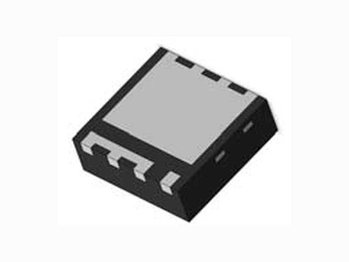
2SK3050DFN KEXIN
Document overview
- Manufacturer or author: Provided By digicamel.com
- PDF pages: 6
Technical content
www.kexin.com.cn 1 MOSFETSMD Type N-Channel MOSFET 2SK3050DFN DFN2x2C-8L Ƶ Features ƽ VDS =1 0 0V ƽ ID (at VGS =1 0V )=8A ƽ RDS(ON) (at VGS =1 0V )<3 2m ȍ ƽ RDS(ON) (at VGS =4 . 5V )<3 9m ȍ Ƶ Absolute Maximum Ratings (TA =2 5ć unless otherwise noted) Symbol Rating Unit VDS 100 VGS ±20 TA=25ć 8 TA=70ć 6 IDM 32 TA=25ć 4.1 TA=70ć 2.6 Thermal Resistance.Junction- to-AmbientA t İ 10s 30 Thermal Resistance.Junction- to-AmbientAD Steady-State 55 TJ 150 Tstg -55 to 150 PD RthJA Parameter Drain-Source Voltage Gate-Source Voltage A WPower Dissipation B ć/W Pulsed Drain CurrentC V ć Junction Temperature Storage Temperature Range Continuous Drain Current I D D S G Pin1 Pin1 D S G
www.kexin.com.cn2 MOSFETSMD Type N-Channel MOSFET 2SK3050DFN Ƶ Electrical Characteristics (TJ =2 5ć unless othewise specified) Parameter Symbol Min Typ Max Unit Drain-Source Breakdown Voltage BV DSS 100 V Gate to Source Leakage Current I GSS ±100 nA Gate to Source Threshold Voltage V GS(th) 1.4 2.4 V Forward Transconductance g FS 25 S Input Capacitance C iss 840 Output Capacitance C oss 64 Reverse Transfer Capacitance C rss 4 Gate Resistance R g 1.4 ȍ Total Gate Charge Q g(10V) 12.8 25 Total Gate Charge Q g(4.5V) 6.1 12 Gate Source Charge Q gs 2.1 Gate Drain Charge Q gd 1.8 Output Charge Q oss 11 Turn-On DelayTime t d(on) 7 Turn-On Rise Time t r 8 Turn-Off DelayTime t d(off) 24 Turn-Off Fall Time t f 3 Body Diode Reverse Recovery Time t rr 20 Body Diode Reverse Recovery Charge Q rr 70 nC Maximum Body-Diode Continuous Current I S 5A Diode Forward Voltage V SD 1V Notes: A. The value of RșJA is measured with the device mounted on 1in2 FR-4 board with 2oz. Copper, in a still air environment with TA=25°C. The value in any given application depends on the user's specific board design. B. The power dissipation PD is based on TJ(MAX)=150°C, usingİ10s junction-to-case thermal resistance. C. Repetitive rating, pulse width limited by junction temperature TJ(MAX)=150°C. Ratings are based on low frequency and duty cycles to keep initial TJ=25°C D. The RșJA is the sum of the thermal impedance from junction to lead RșJL and case to ambient. E. The static characteristics in Figures 1 to 6 are obtained using <300ȝs pulses, duty cycle 0.5% max. F. These curves are based on the junction-to-ambient thermal impedance which is measured with the device mounted on 1in2 FR-4 board with 2oz Copper, assuming a maximum junction temperature of TJ(MAX)=150°C. The SOA curve provides a single pulse rating. ȝA ns VGS =0V ,I S =1A VGS =0V , V DS =5 0V , f=1M H z VGS =1 0 V , VDS =5 0V , R L =5 . 8 5ȍ, RGEN=3 ȍ IF =8A , d I/dt =5 0 0A /ȝs mȍ VDS =5V , I D =8A VGS =1 0 V , VDS =5 0V ,I D =8A RDS(On) VGS =1 0V ,I D =8A VGS =4 . 5V ,ID =6A Test Conditions ID = 250 ȝA, V GS =0 V VDS =1 0 0V , VGS =0V VGS =1 0V ,I D =8A , T J =1 2 5ć VGS=0V, VDS=50V nC pF Zero Gate Voltage Drain Current I DSS VDS =1 0 0V , VGS =0V ,T J =5 5 ć VGS =0V , V DS =0V , f=1M H z VDS =0V , V GS =± 2 0V VDS =V GS ,I D =2 5 0ȝA Static Drain-Source On-Resistance
www.kexin.com.cn 3 MOSFETSMD Type N-Channel MOSFET 2SK3050DFN Ƶ Typical Electrical and Thermal Characteristics
www.kexin.com.cn4 MOSFETSMD Type N-Channel MOSFET 2SK3050DFN
www.kexin.com.cn 5 MOSFETSMD Type N-Channel MOSFET 2SK3050DFN
www.kexin.com.cn6 MOSFETSMD Type N-Channel MOSFET 2SK3050DFN Ƶ DFN2x2C-8L Package Outline Dimensions