
DATASHEET SEARCH SITE
Document overview
- Manufacturer or author: Provided By digicamel.com
- PDF pages: 9
Technical content
T4-LDS-0102, Rev. 3 (121485) ©2012 Microsemi Corporation Page 1 of 9 2N7224, 2N7225, 2N7227 and 2N7228 Compliant N-CHANNEL MOSFET Qualified per MIL-PRF-19500/592 Qualified Levels: JAN, JANTX, and JANTXV
DESCRIPTION
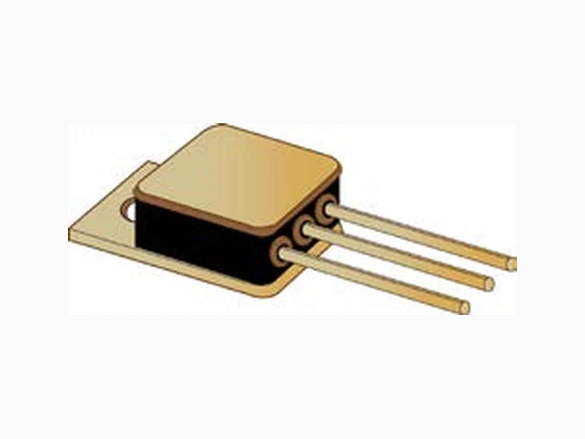
This family of switching transistors is military qualified up to the JANTXV level for high- reliability applications. These devices are also available in a low profile U surface mount package. Microsemi also offers numerous other transistor products to meet higher and lower power ratings with various switching speed requirements in both through-hole and surface- mount packages. Also available in: U (SMD-1 or TO-267AB) package (surface mount) 2N7224U & 2N7228U Important: For the latest information, visit our website http://www.microsemi.com.
FEATURES
- JEDEC registered 2N7224, 2N7225, 2N7227 and 2N7228 number series.
- JAN, JANTX, and JANTXV qualifications are available per MIL-PRF-19500/592. (See part nomenclature for all available options.)
- RoHS compliant by design. APPLICATIONS / BENEFITS
- Low-profile design.
- Military and other high-reliability applications. MAXIMUM RATINGS @ TA = +25ºC unless otherwise stated MSC – Lawrence
6 Lake Street,
Lawrence, MA 01841 Tel: 1-800-446-1158 or (978) 620-2600 Fax: (978) 689-0803 MSC – Ireland Gort Road Business Park, Ennis, Co. Clare, Ireland Tel: +353 (0) 65 6840044 Fax: +353 (0) 65 6822298 Website: www.microsemi.com Parameters / Test Conditions Symbol Value Unit Operating & Storage Junction Temperature Range TJ & Tstg -55 to +150 °C Thermal Resistance Junction-to-Case RӨJC 0.83 oC/W Total Power Dissipation @ TA = +25 °C @ TC = +25 °C (1) PT 150 W Gate-Source Voltage, dc VGS ± 20 V Drain Current, dc @ TC = +25 ºC (2) 2N7224 2N7225 2N7227 2N7228 ID1 34.0 27.4 14.0 12.0 A Drain Current, dc @ TC = +100 ºC (2) 2N7224 2N7225 2N7227 2N7228 ID2 A Off-State Current (Peak Total Value) (3) 2N7224 2N7225 2N7227 2N7228 IDM 136 110 A (pk) Source Current 2N7224 2N7225 2N7227 2N7228 IS 34.0 27.4 14.0 12.0 A NOTES: 1. Derated linearly by 1.2 W/ºC for TC > +25 ºC. 2. The following formula derives the maximum theoretical ID limit. ID is limited by package and internal wires and may also be limited by pin diameter: 3. IDM = 4 x ID1 as calculated in note 2.
T4-LDS-0102, Rev. 3 (121485) ©2012 Microsemi Corporation Page 2 of 9 2N7224, 2N7225, 2N7227 and 2N7228 MECHANICAL and PACKAGING
- CASE: Ceramic and gold over nickel plated steel.
- TERMINALS: Gold over nickel plated tungsten/copper.
- MARKING: Part number, date code, and polarity symbol.
- WEIGHT: 6.5 grams.
- See Package Dimensions on last page. PART NOMENCLATURE JAN 2N7224 Reliability Level JAN = JAN Level JANTX = JANTX Level JANTXV = JANTXV Level Blank = Commercial JEDEC type number (see Electrical Characteristics table) SYMBOLS & DEFINITIONS Symbol Definition di/dt Rate of change of diode current while in reverse-recovery mode, recorded as maximum value. IF Forward current RG Gate drive impedance VDD Drain supply voltage VDS Drain source voltage, dc VGS Gate source voltage, dc
T4-LDS-0102, Rev. 3 (121485) ©2012 Microsemi Corporation Page 3 of 9 2N7224, 2N7225, 2N7227 and 2N7228 ELECTRICAL CHARACTERISTICS @ TA = +25 °C, unless otherwise noted Parameters / Test Conditions Symbol Min. Max. Unit OFF CHARACTERISTICS Drain-Source Breakdown Voltage VGS = 0 V, ID = 1.0 mA 2N7224 2N7225 2N7227 2N7228 V(BR)DSS 100 200 400 500 V Gate-Source Voltage (Threshold) VDS ≥ VGS, ID = 0.25 mA VDS ≥ VGS, ID = 0.25 mA, TJ = +125°C VDS ≥ VGS, ID = 0.25 mA, TJ = -55°C VGS(th)1 VGS(th)2 VGS(th)3 2.0 1.0 4.0 5.0 V Gate Current VGS = ± 20 V, VDS = 0 V VGS = ± 20 V, VDS = 0 V, TJ = +125°C IGSS1 IGSS2 ±100 ±200 nA Drain Current VGS = 0 V, VDS = 80 V VGS = 0 V, VDS = 160 V VGS = 0 V, VDS = 320 V VGS = 0 V, VDS = 400 V 2N7224 2N7225 2N7227 2N7228 IDSS1 µA Drain Current VGS = 0 V, VDS = 80 V, TJ = +125 °C VGS = 0 V, VDS = 160 V, TJ = +125 °C VGS = 0 V, VDS = 320 V, TJ = +125 °C VGS = 0 V, VDS = 400 V, TJ = +125 °C 2N7224 2N7225 2N7227 2N7228 IDSS2 0.25 mA Static Drain-Source On-State Resistance VGS = 10 V, ID = 21.0 A pulsed VGS = 10 V, ID = 17.0 A pulsed VGS = 10 V, ID = 9.0 A pulsed VGS = 10 V, ID = 8.0 A pulsed 2N7224 2N7225 2N7227 2N7228 rDS(on)1 0.070 0.100 0.315 0.415 Ω Static Drain-Source On-State Resistance VGS = 10 V, ID = 34.0 A pulsed VGS = 10 V, ID = 27.4 A pulsed VGS = 10 V, ID = 14.0 A pulsed VGS = 10 V, ID = 12.0 A pulsed 2N7224 2N7225 2N7227 2N7228 rDS(on)2 0.081 0.105 0.415 0.515 Ω Static Drain-Source On-State Resistance TJ = +125°C VGS = 10 V, ID = 21.0 A pulsed VGS = 10 V, ID = 17.0 A pulsed VGS = 10 V, ID = 9.0 A pulsed VGS = 10 V, ID = 8.0 A pulsed 2N7224 2N7225 2N7227 2N7228 rDS(on)3 0.11 0.17 0.68 0.90 Ω Diode Forward Voltage VGS = 0 V, ID = 34.0 A pulsed VGS = 0 V, ID = 27.4 A pulsed VGS = 0 V, ID = 14.0 A pulsed VGS = 0 V, ID = 12.0 A pulsed 2N7224 2N7225 2N7227 2N7228 VSD 1.8 1.9 1.7 1.7 V
T4-LDS-0102, Rev. 3 (121485) ©2012 Microsemi Corporation Page 4 of 9 2N7224, 2N7225, 2N7227 and 2N7228 ELECTRICAL CHARACTERISTICS @ TA = +25 °C, unless otherwise noted (continued) DYNAMIC CHARACTERISTICS Parameters / Test Conditions Symbol Min. Max. Unit Gate Charge: On-State Gate Charge VGS = 10 V, ID = 34.0 A, VDS = 50 V VGS = 10 V, ID = 27.4 A, VDS = 50 V VGS = 10 V, ID = 14.0 A, VDS = 50 V VGS = 10 V, ID = 12.0 A, VDS = 50 V 2N7224 2N7225 2N7227 2N7228 Qg(on) 125 115 110 120 nC Gate to Source Charge VGS = 10 V, ID = 34.0 A, VDS = 50 V VGS = 10 V, ID = 27.4 A, VDS = 50 V VGS = 10 V, ID = 14.0 A, VDS = 50 V VGS = 10 V, ID = 12.0 A, VDS = 50 V 2N7224 2N7225 2N7227 2N7228 Q gs nC Gate to Drain Charge VGS = 10 V, ID = 34.0 A, VDS = 50 V VGS = 10 V, ID = 27.4 A, VDS = 50 V VGS = 10 V, ID = 14.0 A, VDS = 50 V VGS = 10 V, ID = 12.0 A, VDS = 50 V 2N7224 2N7225 2N7227 2N7228 Qgd nC SWITCHING CHARACTERISTICS Parameters / Test Conditions Symbol Min. Max. Unit Turn-on delay time ID = 34.0 A, VGS = 10 V, RG = 2.35 Ω, VDD = 50 V ID = 27.4 A, VGS = 10 V, RG = 2.35 Ω, VDD = 100 V ID = 14.0 A, VGS = 10 V, RG = 2.35 Ω, VDD = 200 V ID = 12.0 A, VGS = 10 V, RG = 2.35 Ω, VDD = 250 V 2N7224 2N7225 2N7227 2N7228 t d(on) ns Rinse time ID = 34.0 A, VGS = 10 V, RG = 2.35 Ω, VDD = 50 V ID = 27.4 A, VGS = 10 V, RG = 2.35 Ω, VDD = 100 V ID = 14.0 A, VGS = 10 V, RG = 2.35 Ω, VDD = 200 V ID = 12.0 A, VGS = 10 V, RG = 2.35 Ω, VDD = 250 V 2N7224 2N7225 2N7227 2N7228 t r 190 ns Turn-off delay time ID = 34.0 A, VGS = 10 V, RG = 2.35 Ω, VDD = 50 V ID = 27.4 A, VGS = 10 V, RG = 2.35 Ω, VDD = 100 V ID = 14.0 A, VGS = 10 V, RG = 2.35 Ω, VDD = 200 V ID = 12.0 A, VGS = 10 V, RG = 2.35 Ω, VDD = 250 V 2N7224 2N7225 2N7227 2N7228 t d(off) 170 ns Fall time ID = 34.0 A, VGS = 10 V, RG = 2.35 Ω, VDD = 50 V ID = 27.4 A, VGS = 10 V, RG = 2.35 Ω, VDD = 100 V ID = 14.0 A, VGS = 10 V, RG = 2.35 Ω, VDD = 200 V ID = 12.0 A, VGS = 10 V, RG = 2.35 Ω, VDD = 250 V 2N7224 2N7225 2N7227 2N7228 tf 130 ns Diode Reverse Recovery Time di/dt ≤ 100 A/µs, VDD ≤ 30 V, IF = 34.0 A di/dt ≤ 100 A/µs, VDD ≤ 30 V, IF = 27.4 A di/dt ≤ 100 A/µs, VDD ≤ 30 V, IF = 14.0 A di/dt ≤ 100 A/µs, VDD ≤ 30 V, IF = 12.0 A 2N7224 2N7225 2N7227 2N7228 trr 500 950 1200 1600 ns
T4-LDS-0102, Rev. 3 (121485) ©2012 Microsemi Corporation Page 5 of 9 2N7224, 2N7225, 2N7227 and 2N7228 GRAPHS t1, Rectangle Pulse Duration (seconds) FIGURE 1 Thermal Impedance Curves Thermal Response (ZθJC)
T4-LDS-0102, Rev. 3 (121485) ©2012 Microsemi Corporation Page 6 of 9 2N7224, 2N7225, 2N7227 and 2N7228 GRAPHS (continued) FIGURE 2 – Maximum Drain Current vs Case Temperature Graphs TC CASE TEMPERATURE (ºC) TC CASE TEMPERATURE (ºC) For 2N7224 For 2N7225 TC CASE TEMPERATURE (ºC) TC CASE TEMPERATURE (ºC) For 2N7227 For 2N7228 ID DRAIN CURRENT (AMPERES) ID DRAIN CURRENT (AMPERES) ID DRAIN CURRENT (AMPERES) ID DRAIN CURRENT (AMPERES)
T4-LDS-0102, Rev. 3 (121485) ©2012 Microsemi Corporation Page 7 of 9 2N7224, 2N7225, 2N7227 and 2N7228 GRAPHS (continued) FIGURE 3 – Maximum Safe Operating Area VDS, DRAIN-TO-SOURCE VOLTAGE (VOLTS) for 2N7224 VDS, DRAIN-TO-SOURCE VOLTAGE (VOLTS) for 2N7225 ID, DRAIN CURRENT (AMPERES) ID, DRAIN CURRENT (AMPERES)
T4-LDS-0102, Rev. 3 (121485) ©2012 Microsemi Corporation Page 8 of 9 2N7224, 2N7225, 2N7227 and 2N7228 GRAPHS (continued) VDS, DRAIN-TO-SOURCE VOLTAGE (VOLTS) for 2N7227 VDS, DRAIN-TO-SOURCE VOLTAGE (VOLTS) for 2N7228 ID DRAIN CURRENT (AMPERES) ID DRAIN CURRENT (AMPERES)
T4-LDS-0102, Rev. 3 (121485) ©2012 Microsemi Corporation Page 9 of 9 2N7224, 2N7225, 2N7227 and 2N7228 PACKAGE DIMENSIONS NOTES: Dimensions Notes 1. Dimensions are in inches. 2. Millimeters are given for general information only. 3. Glass meniscus included in dimension D and E. 4. All terminals are isolated from case. 5. In accordance with ASME Y14.5M, diameters are equivalent to Φx symbology. Ltr Inch Millimeters Min Max Min Max BL .535 .545 13.59 13.84 CH .249 .260 6.32 6.60 LD .035 .045 0.89 1.14 LL .510 .570 12.95 14.48 LO .150 BSC 3.81 BSC LS .150 BSC 3.81 BSC MHD .139 .149 3.53 3.78 MHO .665 .685 16.89 17.40 TL .790 .800 20.07 20.32 3, 4 TT .040 .050 1.02 1.27 TW .535 .545 13.59 13.84 3, 4 Term 1 Drain Term 2 Source Term 3 Gate