
DATASHEET SEARCH SITE
Document overview
- Manufacturer or author: Provided By digicamel.com
- PDF pages: 7
Technical content
T4-LDS-0097, Rev. 3 (120714) ©2012 Microsemi Corporation Page 1 of 7 1N6036(A) thru 1N6072(A) Available on commercial versions
1500 WATT BIDIRECTIONAL
TRANSIENT VOLTAGE SUPPESSOR Qualified per MIL-PRF-19500/507 Qualified Levels: JAN, JANTX, and JANTXV
DESCRIPTION
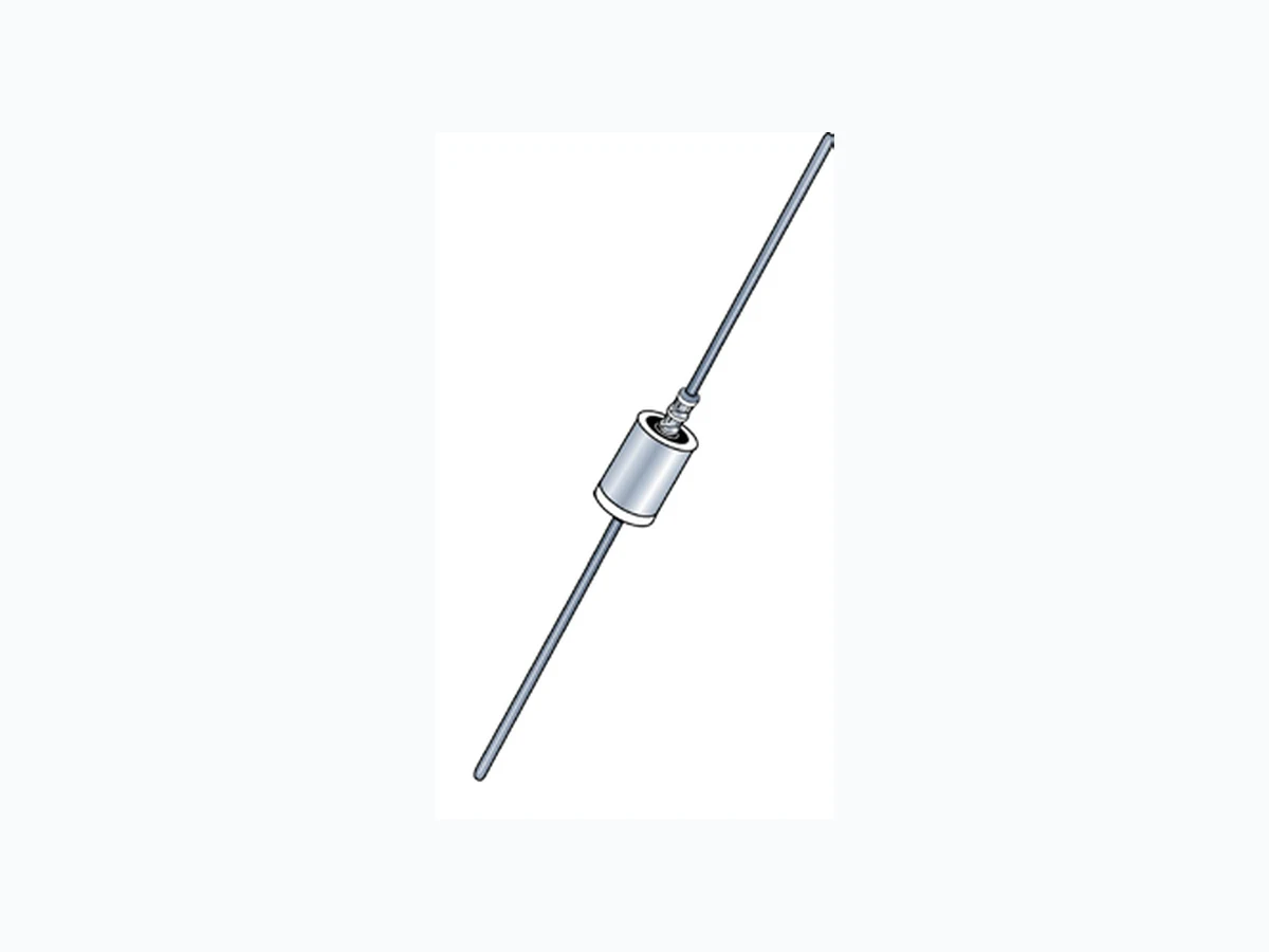
DO-13 (DO-202AA) Package Also available in: DO-13 package (unidirectional) 1N5629 – 1N5665A Case 1 package (plastic equivalent) 1.5KE6.8C – 1.5KE220CA DO-215AB package (Gull-wing) SMCG5.0 – SMCG170A DO-214AB package (J-bend) SMCJ5.0 – SMCJ170A MSC – Lawrence
6 Lake Street,
Lawrence, MA 01841 Tel: 1-800-446-1158 or (978) 620-2600 Fax: (978) 689-0803 MSC – Ireland Gort Road Business Park, Ennis, Co. Clare, Ireland Tel: +353 (0) 65 6840044 Fax: +353 (0) 65 6822298 Website: www.microsemi.com This popular Transient Voltage Suppressor (TVS) series for 1N6036 thru 1N6072A are JEDEC registered selections for bidirectional devices. All have the same high Peak Pulse Power rating of 1500 W with extremely fast response times. They are also available in military qualified selections as described in the “Features” section herein. They are most often used for protecting against transients from inductive switching environments, induced RF effects, or induced secondary lightning effects as found in lower surge levels of IEC61000-4-5. They are also very successful in protecting airborne avionics and electrical systems. Since their response time is virtually instantaneous, they can also protect from ESD and EFT per IEC61000-4-2 and IEC61000-4-4. Important: For the latest information, visit our website http://www.microsemi.com.
FEATURES
- Bidirectional TVS series in axial packages for thru-hole mounting.
- Suppresses transients up to 1500 watts @ 10/1000 µs (see Figure 1).
- Clamps transients in less than 100 pico seconds.
- Working voltage (VWM) range 5.5 V to 185 V.
- Hermetically sealed DO-13 metal package.
- JAN, JANTX, JANTXV military qualifications also available per MIL-PRF-19500/507 for the tighter tolerance “A” suffix types by adding the JAN, JANTX, or JANTXV prefix, e.g. JANTXV1N6036A, etc.
- RoHS compliant versions available (commercial grade only). APPLICATIONS / BENEFITS
- Protection from switching transients and induced RF.
- Protection from ESD & EFT per IEC 61000-4-2 and IEC 61000-4-4.
- Secondary lightning protection per IEC61000-4-5 with 42 Ohms source impedance: Class 1: 1N6036 to 1N6072A Class 2: 1N6036 to 1N6067A Class 3: 1N6036 to 1N6061A Class 4: 1N6036 to 1N6054A
- Secondary lightning protection per IEC61000-4-5 with 12 Ohms source impedance: Class 1: 1N6036 to 1N6064A Class 2: 1N6036 to 1N6057A Class 3: 1N6036 to 1N6049A Class 4: 1N6036 to 1N6042A
- Secondary lightning protection per IEC61000-4-5 with 2 Ohms source impedance: Class 2: 1N6036 to 1N6048A Class 3: 1N6036 to 1N6041A
- Inherently radiation hard as described in Microsemi “MicroNote 050”.
T4-LDS-0097, Rev. 3 (120714) ©2012 Microsemi Corporation Page 2 of 7 1N6036(A) thru 1N6072(A) MAXIMUM RATINGS Parameters/Test Conditions Symbol Value Unit Junction and Storage Temperature TJ and TSTG -55 to +175 ºC Peak Pulse Power @ TL = +25 ºC (1) PPP 1500 W Rated Average Power Dissipation @ TL ≤ +125 ºC (2) PM(AV) 1 W Solder Temperature @ 10 s TSP 260 oC Notes: 1. At 10/1000 us with repetition rate of 0.01% or less (see Figures 1, 2, & 4). 2. At 10 mm from body (see derating in Figure 3 and note below). MECHANICAL and PACKAGING
- CASE: DO-13 (DO-202AA), welded, hermetically sealed metal and glass.
- TERMINALS: All external metal surfaces are tin-lead plated and solderable per MIL-STD-750 method 2026.
- MARKING: Part number.
- POLARITY: Not applicable for bidirectional TVS.
- TAPE & REEL option: Standard per EIA-296 (add “TR” suffix to part number). Consult factory for quantities.
- WEIGHT: Approx 1.4 grams.
- See Package Dimensions on last page. PART NOMENCLATURE JAN 1N6036 A (e3) Reliability Level JAN = JAN level JANTX = JANTX level JANTXV = JANTXV level (All of the above r equire “A” suffix) Blank = Commercial JEDEC type number (See Electrical Characteristics table) RoHS Compliance e3 = RoHS compliant (available on commercial grade only) Blank = non-RoHS compliant Voltage Tolerance A = 5% Blank = 10% SYMBOLS & DEFINITIONS Symbol Definition VWM Standoff Voltage: Applied Reverse Voltage to assure a nonconductive condition. V(BR) Breakdown Voltage: This is the Breakdown Voltage the device will exhibit at 25 oC. VC Maximum Clamping Voltage: The maximum peak voltage appearing across the TVS when subjected to the peak pulse current in a one millisecond time interval. The peak pulse voltage is the combination of voltage rise due to both the series resistance and thermal rise and positive temperature coefficient (αV(BR)). IPP Peak Pulse Current: The peak current during the impulse. (See Figure 2) PPP Peak Pulse Power: The pulse power as determined by the product of VC and IPP. ID Standby Current: The current at the standoff voltage (VWM). I(BR) Breakdown Current: The current used for measuring Breakdown Voltage (V(BR)).
T4-LDS-0097, Rev. 3 (120714) ©2012 Microsemi Corporation Page 3 of 7 1N6036(A) thru 1N6072(A) ELECTRICAL CHARACTERISTICS @ 25 oC (Test Both Polarities) JEDEC Type No. Rated Standoff Voltage VWM Breakdown Voltage V(BR) Maximum Clamping Voltage VC @ IPP Maximum Standby Current ID @ VWM Maximum Peak Pulse Current IPP (See Fig. 2) Maximum Temperature Coefficient of V(BR) V(BR)min V(BR)max @ I(BR) Volts Volts Volts mA Volts µA Amps αV(BR) %/oC 1N6036 *1N6036A 1N6037 *1N6037A 5.5 6.0 6.5 7.0 6.75 7.13 7.38 7.79 8.25 7.88 9.02 8.61 11.7 11.3 12.5 12.1 1000 1000 500 500 128 132 120 124 .061 .061 .065 .065 1N6038 *1N6038A 1N6039 *1N6039A 7.0 7.5 8.0 8.5 8.19 8.65 9.0 9.5 10.00 9.55 11.0 10.5 13.8 13.4 15.0 14.5 200 200 109 112 100 103 .068 .068 .073 .073 1N6040 *1N6040A 1N6041 *1N6041A 8.5 9.0 9.0 10.0 9.9 10.5 10.8 11.4 12.1 11.6 13.2 12.6 16.2 15.6 17.3 16.7 .075 .075 .078 .078 1N6042 *1N6042A 1N6043 *1N6043A 10.0 11.0 11.0 12.0 11.7 12.4 13.5 14.3 14.3 13.7 16.5 15.8 19.0 18.2 22.0 21.2 .081 .081 .084 .084 1N6044 *1N6044A 1N6045 *1N6045A 12.0 13.0 14.0 15.0 14.4 15.2 16.2 17.1 17.5 16.8 19.8 18.9 23.5 22.5 26.5 25.2 56.5 59.5 .086 .086 .088 .088 1N6046 *1N6046A 1N6047 *1N6047A 16.0 17.0 17.0 18.0 18.0 19.0 19.8 20.9 22.0 21.0 24.2 23.1 29.1 27.7 31.9 30.6 51.5 .090 .090 .092 .092 1N6048 *1N6048A 1N6049 *1N6049A 19.0 20.0 21.0 22.0 21.6 22.8 24.3 25.7 26.4 25.2 29.7 28.4 34.7 33.2 39.1 37.5 38.5 .094 .094 .095 .096 1N6050 *1N6050A 1N6051 *1N6051A 24.0 25.0 26.0 28.0 27.0 28.5 29.7 31.4 33.0 31.5 36.3 34.7 43.5 41.4 47.7 45.7 34.5 31.5 .097 .097 .098 .098 1N6052 *1N6052A 1N6053 *1N6053A 29.0 30.0 31.0 33.0 32.4 34.2 35.1 37.1 39.6 37.8 42.9 41.0 52.0 49.9 56.4 53.9 26.5 .099 .099 .100 .100 1N6054 *1N6054A 1N6055 *1N6055A 34.0 36.0 38.0 40.0 38.7 40.9 42.3 44.7 47.3 45.2 51.7 49.4 61.9 59.3 67.8 64.8 25.3 22.2 23.2 .101 .101 .101 .101 1N6056 *1N6056A 1N6057 *1N6057A 41.0 43.0 45.0 47.0 45.9 48.5 50.4 53.2 56.1 53.6 61.6 58.8 73.5 70.1 80.5 77.0 20.4 21.4 18.6 19.5 .102 .102 .103 .103 1N6058 *1N6058A 1N6059 *1N6059A 48.0 53.0 55.0 58.0 55.8 58.9 61.2 64.6 68.2 65.1 74.8 71.4 89.0 85.0 98.0 92.0 16.9 17.7 15.3 16.3 .104 .104 .104 .104 1N6060 *1N6060A 1N6061 *1N6061A 60.0 64.0 66.0 70.0 67.5 71.3 73.8 77.9 82.5 78.8 90.2 86.1 108.0 103.0 118.0 113.0 13.9 14.6 12.7 13.3 .105 .105 .105 .105
T4-LDS-0097, Rev. 3 (120714) ©2012 Microsemi Corporation Page 4 of 7 1N6036(A) thru 1N6072(A) ELECTRICAL CHARACTERISTICS @ 25 oC (Test Both Polarities) JEDEC Type No. Rated Standoff Voltage VWM Breakdown Voltage V(BR) Maximum Clamping Voltage VC @ IPP Maximum Standby Current ID @ VWM Maximum Peak Pulse Current IPP (See Fig. 2) Maximum Temperature Coefficient of V(BR) V(BR)min V(BR)max @ I(BR) Volts Volts Volts mA Volts µA Amps αV(BR) %/oC 1N6062 *1N6062A 1N6063 *1N6063A 73.0 75.0 81.0 82.0 81.9 86.5 90.0 95.0 100.0 95.5 110.0 105.0 131.0 125.0 144.0 137.0 11.4 12.0 10.4 11.0 .106 .106 .106 .106 1N6064 *1N6064A 1N6065 *1N6065A 90.0 94.0 95.0 100.0 99.0 105.0 108.0 114.0 121.0 116.0 132.0 126.0 158.0 152.0 176.0 168.0 9.5 9.9 8.5 8.9 .107 .107 .107 .107 1N6066 *1N6066A 1N6067 *1N6067A 105.0 110.0 121.0 128.0 117.0 124.0 135.0 143.0 143.0 137.0 165.0 158.0 191.0 182.0 223.0 213.0 7.8 8.2 6.7 7.0 .107 .107 .108 .108 1N6068 *1N6068A 1N6069 *1N6069A 137.0 145.0 145.0 150.0 153.0 162.0 162.0 171.0 187.0 179.0 198.0 189.0 258.0 245.0 274.0 261.0 5.8 6.1 5.5 5.7 .108 .108 .108 .108 1N6070 *1N6070A 1N6071 *1N6071A 155.0 160.0 165.0 170.0 171.0 181.0 180.0 190.0 210.0 200.0 220.0 210.0 292.0 278.0 308.0 294.0 5.1 5.4 4.9 5.1 .108 .108 .108 .108 1N6072 *1N6072A 175.0 185.0 198.0 209.0 242.0 231.0 344.0 328.0 4.3 4.6 .108 .108 * Also available in military qualified types by adding the prefix JAN, JANTX or JANTXV per MIL-PRF-19500/507.
T4-LDS-0097, Rev. 3 (120714) ©2012 Microsemi Corporation Page 7 of 7 1N6036(A) thru 1N6072(A) PACKAGE DIMENSIONS NOTES: 1 Dimensions are in inches. 2 Millimeter equivalents are given for general information only. 3 The major diameter is essentially constant along its length.
4 Within this zone, diameter may vary to allow for lead finishes and
irregularities.
5 Dimension to allow for pinch or seal deformation anywhere along
tubulation. 6 Symbol for bidirectional transient suppressor. 7 Lead 1 shall be electrically connected to the case. 8 In accordance with ASME Y14.5M, diameters are equivalent to Φx symbology. Dimensions Symbol Inches Millimeters Notes Min Max Min Max BD .215 .235 5.46 5.97 BL .293 .357 7.44 9.07 3 BLT .570 14.48 CD .045 .100 1.14 2.54 5 LD .025 .035 0.64 0.89 LL 1.000 1.625 25.40 41.28 LU .188 4.78 4