
2N6790U MICROSEMI
Document overview
- Manufacturer or author: Provided By digicamel.com
- PDF pages: 7
Technical content
T4-LDS-0229-1, Rev. 1 (120717) ©2012 Microsemi Corporation Page 1 of 7 2N6790U Available on commercial versions N-CHANNEL MOSFET Qualified per MIL-PRF-19500/555 Qualified Levels: JAN, JANTX, and JANTXV
DESCRIPTION
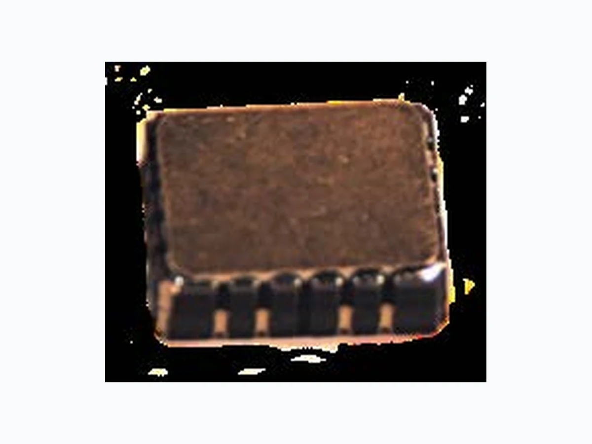
This 2N6790U device is military qualified up to a JANTXV level for high-reliability applications. Microsemi also offers numerous other products to meet higher and lower power voltage regulation applications. U-18 LCC Package Also available in: (leaded) 2N6790U Important: For the latest information, visit our website http://www.microsemi.com.
FEATURES
- JEDEC registered 2N6790U.
- JAN, JANTX, and JANTXV qualification per MIL-PRF-19500/555 available.
- RoHS compliant versions available (commercial grade only). APPLICATIONS / BENEFITS
- High frequency operation.
- Lightweight package.
- ESD to class 1A. MAXIMUM RATINGS @ TC = +25 °C unless otherwise noted MSC – Lawrence
6 Lake Street,
Lawrence, MA 01841 Tel: 1-800-446-1158 or (978) 620-2600 Fax: (978) 689-0803 MSC – Ireland Gort Road Business Park, Ennis, Co. Clare, Ireland Tel: +353 (0) 65 6840044 Fax: +353 (0) 65 6822298 Website: www.microsemi.com Parameters / Test Conditions Symbol Value Unit Junction & Storage Temperature TJ , Tstg -55 to +150 °C Thermal Resistance Junction-to-Case RӨJC 8.93 ºC/W Drain to Gate Voltage VDG 200 V Drain – Source Voltage VDS 200 V Gate – Source Voltage VGS ± 20 V Continuous Drain Current @ TC = +25 °C ID1 2.8 A Continuous Drain Current @ TC = +100 °C ID2 1.8 A Off-State Power Dissipation (1) PD1 14 W Source Current – Drain Diode (Forward Biased VSD) IS 2.8 A Off-State Current IDM 11 A (pk) Drain to Source On State Resistance (2) rDS(on) 0.80 Ω Notes: 1. Derated linearly by 0.11 W/°C for T C > +25 °C. 2. VGS = 10 V, ID = 1.8 A
T4-LDS-0229-1, Rev. 1 (120717) ©2012 Microsemi Corporation Page 2 of 7 2N6790U MECHANICAL and PACKAGING
- CASE: Ceramic LCC-18 with kovar gold plated lid.
- TERMINALS: Gold plating over nickel.
- MARKING: Manufacturer's ID, part number, date code, ESD symbol at Pin 1 location.
- POLARITY: See pad layout.
- TAPE & REEL option: Standard per EIA-481-D. Consult factory for quantities.
- See Package Dimensions on last page. PART NOMENCLATURE JAN 2N6790 U (e3) Reliability Level JAN=JAN level JANTX=JANTX level JANTXV=JANTXV level Blank = Commercial JEDEC type number RoHS Compliance e3 = RoHS compliant (available on commercial grade only) Blank = non-RoHS compliant Surface Mount package SYMBOLS & DEFINITIONS Symbol Definition ID Drain current. IF Forward current. TC Case temperature. VDD Drain supply voltage. VDS Drain to source voltage. VGS Gate to source voltage.
T4-LDS-0229-1, Rev. 1 (120717) ©2012 Microsemi Corporation Page 3 of 7 2N6790U ELECTRICAL CHARACTERISTICS @ TA = +25 °C, unless otherwise noted Parameters / Test Conditions Symbol Min. Max. Unit OFF CHARACTERTICS Drain-Source Breakdown Voltage VGS = 0 V, ID = 1 mA V(BR)DSS 200 V Gate-Source Voltage (Threshold) VDS ≥ VGS, ID = 0.25 mA VDS ≥ VGS, ID = 0.25 mA, Tj = +125 °C VDS ≥ VGS, ID = 0.25 mA, Tj = -55 °C VGS(th)1 VGS(th)2 VGS(th)3 2.0 1.0 4.0 5.0 V Gate Current VGS = ±20 V, VDS = 0 V VGS = ±20 V, VDS = 0 V, Tj = +125 °C IGSS1 IGSS2 ±100 ±200 nA Parameters / Test Conditions Symbol Min. Max. Unit ON CHARACTERTICS Drain Current VGS = 0 V, VDS = 160 V VGS = 0 V, VDS = 160 V, Tj = +125 °C IDSS1 IDSS2 0.25 µA mA Static Drain-Source On-State Resistance VGS = 10 V, ID = 1.8 A pulsed rDS(on)1 0.80 Ω VGS = 10 V, ID = 2.8 A pulsed rDS(on)2 0.85 Ω Tj = +125°C VGS = 10 V, ID = 1.8 A pulsed rDS(on)3 1.50 Ω Diode Forward Voltage VGS = 0 V, ID = 2.8 A pulsed VSD 1.5 V DYNAMIC CHARACTERISTICS Parameters / Test Conditions Symbol Min. Max. Unit Gate Charge: nC On-State Gate Charge Gate to Source Charge Gate to Drain Charge Qg(on) Qgs Qgd 14.3 3.0 9.0 SWITCHING CHARACTERISTICS Parameters / Test Conditions Symbol Min. Max. Unit Switching time tests: Turn-on delay time Rinse time Turn-off delay time Fall time ID = 2.8A, VGS = 10 V Gate drive impedance = 7.5 Ω, VDD = 74 V td(on) tr td(off) tf ns Diode Reverse Recovery Time di/dt = 100 A/µs, V DD ≤ 50 V, ID = ID1 = 2.8 A trr 400 ns
T4-LDS-0229-1, Rev. 1 (120717) ©2012 Microsemi Corporation Page 5 of 7 2N6790U GRAPHS (continued) VDS, DRAIN-TO-SOURCE VOLTAGE (VOLTS) Figure 3 Maximum Safe Operating Area ID DRAIN CURRENT (AMPERES)
T4-LDS-0229-1, Rev. 1 (120717) ©2012 Microsemi Corporation Page 6 of 7 2N6790U PACKAGE DIMENSIONS Dimensions Ltr Inches Millimeters Min Max Min Max BL .345 .360 8.77 9.14 BW .280 .295 7.12 7.49 CH .095 .115 2.42 2.92 LL1 .040 .055 1.02 1.39 LL2 .055 .065 1.40 1.65 LS .050 BSC 1.27 BSC LS1 .025 BSC 0.635 BSC LS2 .008 BSC 0.203 BSC LW .020 .030 0.51 0.76 Q1 .105 REF 2.67 REF Q2 .120 REF 3.05 REF Q3 .045 .055 1.14 1.40 TL .070 .080 1.78 2.03 TW .120 .130 3.05 3.30 NOTES: 1. Dimensions are in inches. 2. Millimeters are given for general information only. 3. In accordance with ASME Y14.5M, diameters are equivalent to Φx symbology.
T4-LDS-0229-1, Rev. 1 (120717) ©2012 Microsemi Corporation Page 7 of 7 2N6790U PAD LAYOUT PAD ASSIGNMENTS