
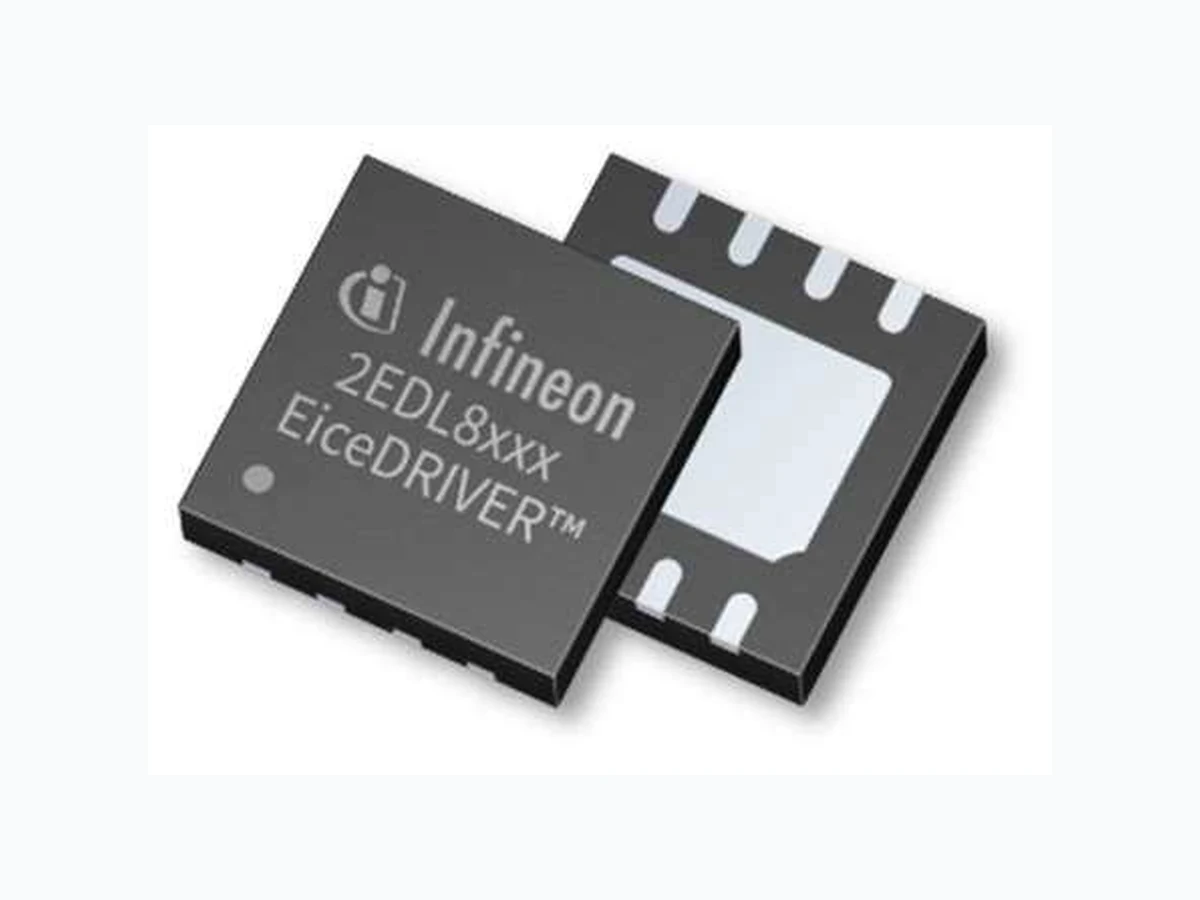
2EDL8X2X INFINEON
Document overview
- Manufacturer or author: Provided By digicamel.com
- PDF pages: 26
Technical content
Features
Level-shift high-side low-side dual channel driver (2EDL802x) Independently controlled high-side and low-side gate drivers (2EDL812x) Differential input for superb robustness with inherent shoot-through protection 3 A (2EDL8x23) or 4 A (2EDL8x24) source current capability for both high side and low side drivers Strong 5 A high side / 6 A low side sink current capability 120 V on-chip bootstrap diode Support operating frequency up to 1 MHz VDD/VHB under voltage lockout (UVLO) -10 V to 20 V Input pin capability for increased robustness (2EDL812x) -8 V to 15 V input pin common mode rejection -5 A output pin reverse current capability 8 V to 17 V supply voltage operating range Feature Comparison Fast propagation delay <6 ns delay matching Offered in VDSON-8 (4 mm x 4 mm) and VSON-10 (3 mm x 3mm) package Lead free RoHS compliant package Potential Applications Typical Application Diagram DC-to-DC converter Isolated bus converter Synchronous rectification for SMPS Class-D Audio Amplifiers Product Validation Qualified for industrial applications according to the relevant tests of JEDEC47/20/22
Description
2EDL8x2x is a high-side low-side driver designed for advanced switching converters such as in telecom and datacom applications. 2EDL802x takes in independent inputs with built-in hysteresis for enhanced noise immunity, whereas 2EDL812x takes in differential input with built-in hysteresis for enhanced noise immunity. 2EDL812x’s inherent shoot-through protection ensures the robustness of the system. 6 ns maximum delay matching ensures volt-second balance and avoids magnetic core saturation.
Datasheet 2 Rev. 2.8 2022.06.29 EiceDRIVERTM 2EDL8x2x
120 V Boot, 3 A / 4 A, Junction-Isolated High Side and Low Side Gate Driver ICs
Datasheet 3 Rev. 2.8 2022.06.29 EiceDRIVERTM 2EDL8x2x
Package Information
1 Package Information
1.1 Ordering Information
Base Part Number Package Type Standard Pack Orderable Part Number Form Quantity 2EDL8023G PG-VDSON-8-4 Tape and Reel 6000 2EDL8023GXUMA1 2EDL8023G3C PG-VSON-10-4 Tape and Reel 3000 2EDL8023G3CXUMA1 2EDL8024G PG-VDSON-8-4 Tape and Reel 6000 2EDL8024GXUMA1 2EDL8024G3C PG-VSON-10-4 Tape and Reel 3000 2EDL8024G3CXUMA1 2EDL8123G PG-VDSON-8-4 Tape and Reel 6000 2EDL8123GXUMA1 2EDL8123G3C PG-VSON-10-4 Tape and Reel 3000 2EDL8123G3CXUMA1 2EDL8124G PG-VDSON-8-4 Tape and Reel 6000 2EDL8124GXUMA1 2EDL8124G3C PG-VSON-10-4 Tape and Reel 3000 2EDL8124G3CXUMA1
1.2 Pin Configuration and Descriptions
Figure 1 Pin Configuration of PG-VDSON-8-4, Top Transparent View
Datasheet 4 Rev. 2.8 2022.06.29 EiceDRIVERTM 2EDL8x2x Figure 2 Pin Configuration of PG-VSON-10-4, Top Transparent View Pin Name VDSON-8 Pin # VSON-10 Pin # Pin Description VDD 1 1 Gate drive supply N/C --- 2,6 Not Connected HB 2 3 High-side gate driver bootstrap rail HO 3 4 High-side gate driver output HS 4 5 High-side FET source connection HI 5 7 High-side driver control input LI 6 8 Low-side driver control input VSS 7 9 Ground return, internally connected to exposed pad LO 8 10 low-side gate driver output
Datasheet 5 Rev. 2.8 2022.06.29 EiceDRIVERTM 2EDL8x2x
2 Block Diagram
A simplified functional block diagram is given in the figure below driver driver HV Level Shift PADS VDD HI LI HO LO HS VSS HB PWM_HS PWM_LS HB UVLO EXPOSED PAD 3.3V Regulator POR VDD UVLO BANDGAP REFERENCE POR VDD VDD3V0 LV Level Shift Figure 3 Block Diagram
Datasheet 6 Rev. 2.8 2022.06.29 EiceDRIVERTM 2EDL8x2x
3 Functional Description
The device is a level-shifted 2-channel driver designed to support topologies with high-side and low-side configurations. The high side is level shifted by the combination of an on-chip 120 V rated bootstrap diode and an external bootstrap capacitor. The device provides 3 A (2EDL8x23) or 4 A (2EDL8x24) peak source current capability for both high-side and low-side and a strong 5 A high-side and 6 A low-side sink current capability. This allows driving large power MOSFETs with minimum or optimized switching losses during the transition through the MOSFET's Miller Plateau. 2EDL802x’s input pins support TTL logic levels independently of supply voltage. They are capable to withstand voltages from -10 V to 20 V, allowing the device to interface with a broad range of analog and digital controllers. The input stage features built-in hysteresis for enhanced noise immunity. The low-side and high-side gate drivers are independently controlled and matched to typical 2 ns between the turn on and turn off of each other. 2EDL812x’s input pins support TTL logic levels independently of supply voltage. They are capable to withstand voltages from -10 V to 20 V and ground potential shifts from -8 V to 15 V, allowing the device to interface with a broad range of analog and digital controllers. The input stage features built-in hysteresis for enhanced noise immunity. The low-side and high-side gate drivers are differentially controlled and matched to typical 2 ns between the turn on and turn off of each other. The differential inputs provide inherent shoot-through protection and ensure high-side and low-side outputs are never on at the same time. The switching node (HS pin) is able to handle negative voltages down to –(24 - VDD) V which allows the high-side channel to be protected from inherent negative voltages caused by parasitic inductance and stray capacitance. Under-voltage lockout circuits are provided for both high- and low-side drivers. UVLO protects the system by forcing the output low when the supply voltage is lower than the specified threshold. The following sections describe key functionalities.
3.1 Supply Voltage
The absolute maximum supply voltage is 20 V. The minimum operating supply voltage is set by the under voltage lockout function to a typical default value of 7.0 V. This lockout function protects power MOSFETs from running into linear mode with subsequent high power dissipation.
3.2 Input Stage
2EDL802x device responds to the two inputs signals (HI and LI) independently according to the following truth table. Table 1 2EDL802x Truth Table LI HI LO HO L L L L H L H L L H L H H H H H The high-side and low-side outputs respond to high-side and low-side inputs independently. 2EDL812x device responds to the combination of two inputs signals (HI and LI) according to the following truth table.
Datasheet 7 Rev. 2.8 2022.06.29 EiceDRIVERTM 2EDL8x2x Table 2 2EDL812x Truth Table LI HI LO HO L L L L H L H L L H L H H H L L True differential input comes with inherent shoot through protection by preventing both low and high side to be on at the same time. It also provides noise immunity against ground bounce. The input stage is designed to operate reliably against –8 V / +15 V ground voltage drift. Input logic hysteresis also helps combat disturbances to the input signal. The differential voltage between the two input pins is rated at 8 V maximum because of the back-to-back ESD diodes that connect the two input pins together. Above this voltage, the ESD diodes start clamping which causes a current flow from the high voltage potential input pin to the low voltage potential input pin.
3.3 Driver Outputs
The low output impedances allow fast transition of the load transistor. Specifically, the ultra-low impedance pull down resistances, typically 0.5 Ω for the high side and 0.35 Ω for the low side, keep the gate of the load transistor down during fast transient events – avoiding dv/dt induced re-turn-on.
3.4 Under Voltage Lockout (UVLO)
The under voltage lockout function ensures that the output can be switched to its high level only if the supply voltage exceeds the UVLO rising threshold voltage. Thus it can be guaranteed, that the switch transistor is not switched on if the driving voltage is too low to completely switch on the device, thereby avoiding excessive power dissipation. The UVLO level is set to a typical value of 7.0 V with 0.5 V hysteresis for supply voltage (VDD) and 5.75 V with 0.25 V hysteresis for high side boot voltage (VHB). UVLO threshold trigger is synchronous. The clock gating ensures minimum pulse width set by the controller is obeyed at all times. This increases robustness of the integrated boot diode due to the controllability of the reverse recovery behavior. A 5 us delay time and a PWM synchronization scheme are implemented in the high-side UVLO to ensure that the load transistor is not operated with marginal gate drive voltage which can lead to high power dissipation. The synchronization is done in such a way that the HO output is blocked when UVLO is released while the HI is high. HO is only propagated when the UVLO is released while the HI is low. Figure 4 High-side UVLO implementation
3.5 Minimum Pulse Width
The device responds to input level according to the truth table in section 3.2 as long as the logic signal complies with the minimum pulse width requirement. Signal pulse longer than the minimum allowable input pulse width
Datasheet 8 Rev. 2.8 2022.06.29 EiceDRIVERTM 2EDL8x2x yields valid output. Any output in response to shorter pulses or glitches should be disregarded and filtered out by the user. Under all allowable operation above input minimum pulse width of 40 ns, the output behaves one to one to the input with minimal pulse width distortion. TONOUT TONIN 40 ns 40 ns 100 ns 100 ns Figure 5 Minimum Pulse Width Input-output On-time Transfer Function This diagram is illustrative only with typical value. Actual value and pulse width distortion is subject to process variation. Output pulse width could in some case be shortened or extended to prevent retoggling. See transient detector section below.
3.6 Transient Detector
The transient detector block is designed to prevent re-toggling of the HO output in case of potential instability of the level shifter caused by phase node movement. For example, a fast-rising phase node voltage could pull the power ground (PGND) down. This could result in potential between HI and PGND higher than the rising threshold of the high-side signal. Such a glitch or noise can be picked up by the driver and propagate through which can lead to a shoot-through event, transformer volt-second imbalance, and potential device destruction. The following describes the basic operation of the block. The transient detector monitors the phase node and tracks its movement, and the rate of change over time for both rising and falling edge. Whenever the rate of change is larger than a certain dv/dt threshold1, the transient detector is active and blocks the HO output from changing state. A High-side Input (HI) toggle triggers a decision to change the state, but HO waits until the transient detector’s active state is removed, then the decision is propagated through. Additional propagation delay caused by the transient detector is limited to one-half of the oscillation period, as the signal always propagates through whenever the transient detector sees a peak or valley where dv/dt approaches zero. See link to Understanding the transient detector [1] for more information.
1 Reference slew rate threshold versus temperature under Section 6 Typical Characteristics
Datasheet 9 Rev. 2.8 2022.06.29 EiceDRIVERTM 2EDL8x2x
4 Characteristics
4.1 Absolute Maximum Ratings
Stresses above the values listed under “Absolute Maximum Ratings” may cause permanent damage to the device. This is a stress rating only and functional operation of the device at these or any other conditions above those indicated in the operational sections of this specification is not implied. Exposure to absolute maximum rating conditions may affect device reliability. Symbol Description Min Max Unit VDD Driver Supply Voltage 1 -0.3 20 V VHS Phase Voltage (DC) -1 V HB + 0.3 V Phase Voltage (Repetitive pulse < 100 ns)2 -(24 - V DD) V HB + 0.3 V VHB High Side Bootstrap Voltage2 -0.3 120 V VHI, VLI LI and HI Input Voltage -10 20 V VI Differential Input Voltage 3 --- 8 V VLO Output voltage on LO -0.3 V DD + 0.3 V VHO Output voltage on HO V HS – 0.3 V HB + 0.3 V IOR LO and HO Peak Reverse Current 4 --- 5 A TJ Operating Junction Temperature -40 150 °C TS Storage Temperature -55 150 °C
4.2 ESD Ratings
Symbol Description Value Unit ESDHBM Human Body Model sensitivity as per ANSI/ESDA/JEDEC JS-001 2000 V ESDCDM Charged Device Model sensitivity as per ANSI/ESDA/JEDEC JS-002 1000 V
4.3 Recommended Operating Conditions
The following operating conditions must not be exceeded in order to ensure correct operation and reliability of the device. All parameters specified in the subsequent tables refer to these operating conditions. Symbol Description Min Typ Max Unit VHS Phase Voltage (DC) -1 --- 80 V Phase Voltage (Repetitive pulse < 100 ns) -(24 - V DD) --- 80 V VDD Driver Supply Voltage 8 10 17 V VHB High Side Bootstrap Voltage -0.3 --- 90 V TJ Junction Temperature -40 --- 125 °C dv/dt HS Slew Rate --- --- 50 V/ns VI Differential Input Voltage 0 3.3 5 V VICMR Input Signal Common Mode Rejection (2EDL812x) -8 + V I/2 --- 15 – V I/2 V
1 All voltage ratings in this section referenced to ground
2 Not subject to production test. Verified by design/characterization
3 Absolute voltage difference between HI and LI (|VHI-VLI|)
4 For < 500 ns pulses
Datasheet 10 Rev. 2.8 2022.06.29 EiceDRIVERTM 2EDL8x2x
4.4 Static Electrical Characteristics
VDD = VHB = 12 V, VHS =VSS=0V. TC = 25oC unless otherwise specified. The VIN and IIN parameters are referenced to VSS. Symbol Description Min Typ Max Units Conditions VDDR V DD UVLO Rising Threshold 6.6 7.0 7.4 V VDDH V DD UVLO Threshold Hysteresis --- 0.5 --- V VHBR V HB UVLO Rising Threshold1 5.5 5.75 6.0 V VHBH V HB UVLO Threshold Hysteresis --- 0.27 --- V IHB Boot voltage Quiescent Current --- 0.55 0.7 mA V LI=VHI=0V IHBO Boot voltage Operating Current --- 2.8 3.1 mA f=500kHz, CLOAD=0nF, 2EDL8x23 --- 2.9 3.2 f=500kHz, C LOAD=0nF, 2EDL8x24 IDD V DD Quiescent Current --- 0.55 0.7 mA V LI=VHI=0V IDDO V DD Operating Current --- 2.8 3.1 mA f=500kHz, C LOAD=0nF, 2EDL8x23 --- 2.9 3.2 f=500kHz, C LOAD=0nF, 2EDL8x24 RIN Input Pulldown Resistance 54 68 82 kΩ VIR Rising Input Voltage Threshold 1.6 2.25 2.9 V VIF Falling Input Voltage Threshold 1.0 1.65 2.3 V VIH Input Logic Voltage Hysteresis --- 0.6 --- V RPUH High Side Pull Up Resistance --- 1.45 --- Ω 2EDL8x23 RPDH High Side Pull Down Resistance --- 0.5 --- Ω RPUL Low Side Pull Up Resistance --- 1.45 --- Ω 2EDL8x23 RPDL Low Side Pull Down Resistance --- 0.35 --- Ω
1 HB (high side bootstrap) related ratings referenced to VHS
Datasheet 11 Rev. 2.8 2022.06.29 EiceDRIVERTM 2EDL8x2x
4.5 Dynamic Electrical Characteristics
VDD = VHB = 12 V, VHS =VSS=0V. TC = 25oC unless otherwise specified. Symbol Description Min Typ Max Units Conditions IPUH High Side Peak Pull Up Current 1 --- 3 --- A VHO = 0 V , 2EDL8x23 --- 4 --- V HO = 0 V , 2EDL8x24 IPDH High Side Peak Pull Down Current1 --- 5 --- A V HO = 12 V IPUL Low Side Peak Pull Up Current 1 --- 3 --- A VLO = 0 V , 2EDL8x23 --- 4 --- V LO = 0 V , 2EDL8x24 IPDL Low Side Peak Pull Down Current1 --- 6 --- A V LO = 12 V TDR Rising Propagation Delay2,3 --- 45 54 ns CLOAD = 0 TDF Falling Propagation Delay4,3 --- 45 54 ns CLOAD = 0 TDM Delay Matching 5 --- 2 6 ns TPW Minimum Input Pulse Width 6 --- --- 40 ns TDRR Bootstrap Diode Turn off Time 7 --- 10 --- ns I F = 20 mA, IPRR = 0.5 A
4.6 Thermal Mechanical Characteristics
Symbol Description Min Typ Max Units Conditions RthJC Junction to Case Thermal Resistance VDSON-8 --- 3 --- °C/W Bottom --- 46 --- °C/W Top VSON-10 --- 5.8 --- °C/W Bottom --- 69 --- °C/W Top RthJA Device on PCB VDSON-8 --- 42 --- °C/W 6 cm2 cooling area8 VSON-10 --- 60 --- °C/W 1 Not subject to production test.
2 Rising propagation delay from LI to LO and from HI to HO
3 A transient detector blocks the toggling of the high side output when it detects moving phase node (due to transition and/or oscillation). It prevents unwanted retoggling but may increase propagation delay. See transient detector activation in Figure 7.
4 Falling propagation delay from LI to LO and from HI to HO
5 Consolidated delay matching (1) ON: between LO rising and HO falling and (2) OFF: between LO falling and HO rising
6 Minimum input pulse width that produces valid output signal
7 External schottky boot diode in parallel recommended for high dv/dt application
8 Device on 40 mm x 40 mm x 1.5 mm epoxy PCB FR4 with 6 cm2 (one layer, 70 µm thick) copper area for drain connection. PCB vertical in still air
Datasheet 12 Rev. 2.8 2022.06.29 EiceDRIVERTM 2EDL8x2x
5 Descriptive Illustration
3.3V / 5.0V PGND VDD tLH tHL DtOUT DtIN HI HO VSS 3.3V / 5.0V HS HB Figure 6 Propagation delay Figure 7 UVLO behavior Transient Detector Response Inactive Active Slew-rate Threshold dv/dt Figure 8 Transient Detector Response3
3 Reference slew rate threshold versus temperature under Section 6 Typical Characteristics
Datasheet 13 Rev. 2.8 2022.06.29 EiceDRIVERTM 2EDL8x2x
6 Typical Characteristics
0.1 0.2 0.3 0.4 0.5 0.6 0.7 0.8 7 8 9 10 11 12 13 14 15 16 17 Quiescent Current [mA] VDD [V] Quiescent Current vs. VDD IVDD IHB TJ = 25 °C 1.00E-04 1.00E-03 1.00E-02 1.00E-01 IDIODE [A] VDIODE [V] Diode Current vs. Voltage TJ = 25 °C 0.01 0.02 0.03 0.04 0.05 0.06 0.07 1.00E+04 1.00E+05 1.00E+06 IDD Operating Current [A] Switching Frequency [Hz] IDD Operating Current vs. Temperature 0pF, -40°C 0pF, 25°C 0pF, 150°C 1nF, -40°C 1nF, 25°C 1nF, 150°C 4.7nF, -40°C 4.7nF, 25°C 4.7nF, 150°C VDD = 12 V 0.01 0.02 0.03 0.04 0.05 0.06 0.07 1.00E+04 1.00E+05 1.00E+06 IHB Operating Current [A] Switching Frequency [Hz] IHB Operating Current vs. Temperature 0pF, -40°C 0pF, 25°C 0pF, 150°C 1nF, -40°C 1nF, 25°C 1nF, 150°C 4.7nF, -40°C 4.7nF, 25°C 4.7nF, 150°C VDD = 12 V 0.03 0.06 0.09 0.12 0.15 0.18 0.21 0.24 -50 0 50 100 150 LO Output Votlage @100 mA [V] Junction Temperature [°C] LO Output Voltage (Pull-up) vs. Temperature 2EDL8x24 2EDL8x23 VDD = 12V 0.03 0.06 0.09 0.12 0.15 0.18 0.21 0.24 -50 0 50 100 150 HO Output Votlage @100 mA [V] Junction Temperature [°C] HO Output Voltage (Pull-up) vs. Temperature 2EDL8x24 2EDL8x23 VDD = 12V
Datasheet 14 Rev. 2.8 2022.06.29 EiceDRIVERTM 2EDL8x2x 0.01 0.02 0.03 0.04 0.05 0.06 0.07 0.08 -50 0 50 100 150 LO Output Votlage @100 mA [V] Junction Temperature [°C] LO Output Voltage (Pull-down) vs. Temperature 2EDL8x24 2EDL8x23 VDD = 12V 0.01 0.02 0.03 0.04 0.05 0.06 0.07 0.08 -50 0 50 100 150 HO Output Votlage @100 mA [V] Junction Temperature [°C] HO Output Voltage (Pull-down) vs. Temperature 2EDL8x24 2EDL8x23 VDD = 12V 0.5 1.5 2.5 8 10 12 14 16 18 20 Input Threshold Voltage [V] VDD [V] Input Threshold vs. Supply Voltage Vth_H Vth_L TJ = 25 °C 0.5 1.5 2.5 -50 0 50 100 150 Input Threshold [V] Junction Temperature [°C] Input Threshold vs. Temperature Vth_H Vth_L TJ = 25 °C -50 0 50 100 150 UVLO Threshold [V] Junction Temperature [°C] UVLO Threshold vs. Temperature VTH_rise_hb VTH_fall_hb VTH_rise_vdd VTH_fall_vdd 0.1 0.2 0.3 0.4 0.5 0.6 -50 0 50 100 150 UVLO Thresholds Hysteresis [V] Junction Temperature [°C] UVLO Threshold Hysteresis vs. Temperature HYST_HB HYST_VDD
Datasheet 15 Rev. 2.8 2022.06.29 EiceDRIVERTM 2EDL8x2x -50 0 50 100 150 Propagation Delay [ns] Junction Temperature [°C] Propagation Delay vs. Temperature del_rise_HI_HO del_fall_HI_HO del_rise_LI_LO del_fall_LI_LO VDD = 12 V 40.00 42.00 44.00 46.00 48.00 50.00 52.00 54.00 56.00 5 10 15 20 Propagation Delay [ns] VDD [V] Propagation Delay vs. VDD del_rise_HI_HO del_fall_HI_HO del_rise_LI_LO del_fall_LI_LO TJ = 25 °C -50 0 50 100 150 Delay Matching [ns] Junction Temperature [°C] Delay Matching vs.Temperature del_match_ton del_match_toff VDD = 12 V 0 0.05 0.1 0.15 0.2 0.25 0.3 -50 0 50 100 150 Slew Rate Threshold [V/ns] Junction Temperature [°C] Transient Detector Threshold vs. Temperature nom VDD = 12 V
Datasheet 16 Rev. 2.8 2022.06.29 EiceDRIVERTM 2EDL8x2x Application and Guidelines
7 Application and Guidelines
7.1 Typical Application Diagram
Figure 9 Typical Application 1 – Primary Side Half-bridge Figure 10 Typical Application 2 – Full-bridge Secondary Side Rectification
7.2 Design Guidelines
Figure 11. However, this method imposes limitation on the power converter’s duty cycle due to the selection of the bootstrap components. leakage current is discharing the Cboot during this phase.
Datasheet 18 Rev. 2.8 2022.06.29 EiceDRIVERTM 2EDL8x2x Application and Guidelines Figure 12 Typical Cboot waveform
7.2.1 Bootstrap Capacitor Selection
The bootstrap capacitor provides the necessary charge to drive the high-side mosfet and thus it needs to be sized in such a way that the maximum voltage drop across this capacitor will not fall below the high-side UVLO threshold during transient and normal operations. First, determine the maximum allowable voltage drop (ΔVCboot_max) when the high-side mosfet (Q1) is on which is given by the following formula: Where: Vdd = Gate driver supply voltage VF = Bootstrap diode forward voltage drop with typical value of 1.25 V at IF=100 uA and 2.15 V at IF=100 mA , TJ=25°C VHBR = HB UVLO rising threshold VHBH = HB UVLO threshold hysteresis Next, determine the total charge (QT) that must be delivered by the bootstrap capacitor at maximum duty cycle. As mentioned, there are several factors that contribute to the discharge of the bootstrap capacitor such as the Q1’s total gate charge, Q1’s gate-source leakage current, HB quiescent current, HB leakage current, bootstrap diode reverse bias leakage current and bootstrap capacitor leakage current ( if using an electrolytic capacitor ). For sake of simplicity, only Q1’s total gate charge and HB quiescent and leakage current are considered as the other sources of leakage are negligible in comparison. ?௦௪ ?௦௪ (2) Where: QG = high-side mosfet (Q1) total gate charge IHB = HB maximum quiescent current
Datasheet 19 Rev. 2.8 2022.06.29 EiceDRIVERTM 2EDL8x2x Application and Guidelines IHBS = HB to VSS leakage current with a typical value of 1.25 mA at 90 V HB voltage and TJ=25°C Dmax = maximum duty cycle Fsw = switching frequency The minimum bootstrap capacitor value can then be calculated using the formula: (3)
7.2.2 VDD Bypass Capacitor Selection
The Vdd bypass capacitor provides the charge for the bootstrap capacitor during the charging period. As a rule of thumb, the Vdd bypass capacitor should be sized to be atleast 10~20 times larger than the bootstrap capacitor. This equates to a voltage ripple of 5~10% in the Vdd capacitor.
7.2.3 Bootstrap Resistor Selection
The bootstrap resistor limits the current in the bootstrap diode during start-up when the bootstrap capacitor is initially completely discharged. The peak current through this resistor is given by: ?௧ (5) The bootstrap resistor together with the bootstrap capacitor introduces a time constant and should be sized appropriately to achieve the desired start-up time. For this calculation, it is assumed that the bootstrap capacitor is fully charged after 4 time constant. With this, Rboot can be calculated using the following formula: (6) Where: tmin = minimum on time of the low-side mosfet (Q2)
7.2.4 External Bootstrap Diode Selection
For high dV/dT applications, an external bootstrap diode is recommended to be in parallel with the internal bootstrap diode. A fast recovery or schottky diode with low forward voltage drop is recommended in order to minimize the losses and leakage current. It should be chosen such that it can handle the peak transient current from Equation (5) during start-up conditions and the blocking voltage rating should be higher than the maximum input voltage (Vin) with enough derating.
7.2.5 Gate Resistor Selection
The turn-on and turn-off external gate resistors control the turn-on and turn-off current of the gate driver providing an external way to control the switching speed of the mosfet for purposes such as voltage overshoot control, ringing reduction, EMI mitigation, spurious turn-on protection, shoot –through protection etc. The following formulas shows the effect of the external gate resistor to the output current capability of the gate driver.
Datasheet 20 Rev. 2.8 2022.06.29 EiceDRIVERTM 2EDL8x2x Application and Guidelines (7) (8) (9) (10) Where: IHSRC = High-side peak source current IHSNK = High-side peak sink current ILSRC = Low-side peak source current ILSNK = Low-side peak sink current RPUH = High-side pull-up resistance RPDH = High-side pull-down resistance RPUL = Low-side pull-up resistance RPDL = Low-side pull-down resistance VDD = Gate driver supply voltage VF = Bootstrap diode forward voltage drop RG_HS = High-side external gate resistance RG_LS = Low-side external gate resistance RG_int = Mosfet internal gate resistance For a detailed discussion on how to optimize the gate resistors, a dedicated application note with link in the reference section, e.g. [2], can be viewed.
7.3 PCB Layout Guidelines
In order to maximize the performance of EiceDRIVERTM 2EDL8x2x, below are some recommendations on how to optimize the PCB layout Use a low-ESR decoupling capacitors on VDD-GND and HB-HS and placed it as close as possible to the VDD- GND and HB-HS pins of the driver An option for a series boot resistor is recommended to control the high side mosfet slew rate and therefore the low side mosfet overshoot. The boot loop path including the VDD capacitor, boot diode, boot series resistor and boot capacitor should be as small as possible It is recommended to have an external boot diode placement for high dv/dt application. Placement for gate resistor is also recommended to control the switching speed of the mosfet. Both the gate resistor and the mosfet should be placed as close as possible to the driver in order to minimize the gate loop inductance. Use copper plane underneath the exposed GND pad of the driver and connect it to buried copper plane(s) with multiple thermal vias for better heat dissipation into the PCB. Connection to the HS pin of the driver from the high side mosfet source and low side mosfet drain should be as short and wide as possible and avoid connecting it directly through the high switching current path. LO and HO traces should be as short and wide as possible Avoid letting the LI and HI signal trace to come close to high dV/dT traces which might induce significant noise.
Datasheet 21 Rev. 2.8 2022.06.29 EiceDRIVERTM 2EDL8x2x Application and Guidelines Figure 13 2EDL8x2x Layout Example
Datasheet 22 Rev. 2.8 2022.06.29 EiceDRIVERTM 2EDL8x2x
8 Outline Dimensions
8.1 PG-VDSON-8-4 Package Outline
Figure 14 PG-VDSON-8-4 Outline Dimensions Figure 15 PG-VDSON-8-4 Footprint Dimensions
Datasheet 23 Rev. 2.8 2022.06.29 EiceDRIVERTM 2EDL8x2x
8.2 PG-VSON-10-4 Package Outline
Figure 16 PG-VSON-10-4 Outline Dimensions Figure 17 PG-VSON-10-4 Footprint Dimensions
Datasheet 24 Rev. 2.8 2022.06.29 EiceDRIVERTM 2EDL8x2x
9 Reel and Tape
Reel 330 mm: 6000 pcs/ reel Figure 18 PG-VDSON-8-4 Reel and Tape Figure 19 PG-VSON-10-4 Reel and Tape
Datasheet 25 Rev. 2.8 2022.06.29 EiceDRIVERTM 2EDL8x2x
120 V, 3 A / 4 A, Junction-Isolated High Side and Low Side Gate Driver ICs
10 References
[1] Alan Huang, Understanding the transient detector, Infineon Technologies AG, Neubiberg 2020 [2] A2015-06 EiceDRIVER TM – gate resistor for power devices
120VBoot,3A/4A,Junction-IsolatedHighSideandLowSideGateDriverICs 2EDL8x2x Rev.2.8,2022-09-23 RevisionHistory 2EDL8x2x Revision:2022-09-23,Rev.2.8 Previous Revision Revision Date Subjects (major changes since last revision) 2.2 2020-07-28 Separate table for ESD rating and remove footnote 1 under Abs Max Rating 2.3 2020-10-20 Update footprint, LO/HO Pull-up resistance, LO/HO Output voltage, maximum delay spec, HB operating current and remove external diode in diagrams. 2.4 2020-12-30 Update Tape and Reel specification 2.5 2021-10-11 Include VSON-10 3x3 package details 2.6 2022-04-25 Add repetitive pulse note, minimum DC rating for HS, differential input voltage, minimum input rising threshold, maximum input falling, description leakage current, removed 2EDL812x voltage description, rename "input control" and fix footnote numbering. 2.7 2022-05-12 Update marking pin in Tape and Reel and 3D drawing for PG-VSON-10-4 2.8 2022-09-23 Update UVLO illustration and description. Trademarks Allreferencedproductorservicenamesandtrademarksarethepropertyoftheirrespectiveowners. WeListentoYourComments Anyinformationwithinthisdocumentthatyoufeeliswrong,unclearormissingatall?Yourfeedbackwillhelpustocontinuously improvethequalityofthisdocument.Pleasesendyourproposal(includingareferencetothisdocument)to: erratum@infineon.com Publishedby InfineonTechnologiesAG 81726München,Germany ©2022InfineonTechnologiesAG AllRightsReserved. LegalDisclaimer Theinformationgiveninthisdocumentshallinnoeventberegardedasaguaranteeofconditionsorcharacteristics (“Beschaffenheitsgarantie”). Withrespecttoanyexamples,hintsoranytypicalvaluesstatedhereinand/oranyinformationregardingtheapplicationofthe product,InfineonTechnologiesherebydisclaimsanyandallwarrantiesandliabilitiesofanykind,includingwithoutlimitation warrantiesofnon-infringementofintellectualpropertyrightsofanythirdparty. Inaddition,anyinformationgiveninthisdocumentissubjecttocustomer’scompliancewithitsobligationsstatedinthis documentandanyapplicablelegalrequirements,normsandstandardsconcerningcustomer’sproductsandanyuseofthe productofInfineonTechnologiesincustomer’sapplications. Thedatacontainedinthisdocumentisexclusivelyintendedfortechnicallytrainedstaff.Itistheresponsibilityofcustomer’s technicaldepartmentstoevaluatethesuitabilityoftheproductfortheintendedapplicationandthecompletenessoftheproduct informationgiveninthisdocumentwithrespecttosuchapplication. Information Forfurtherinformationontechnology,deliverytermsandconditionsandpricespleasecontactyournearestInfineon TechnologiesOffice(www.infineon.com). Warnings Duetotechnicalrequirements,componentsmaycontaindangeroussubstances.Forinformationonthetypesinquestion, pleasecontactthenearestInfineonTechnologiesOffice. TheInfineonTechnologiescomponentdescribedinthisDataSheetmaybeusedinlife-supportdevicesorsystemsand/or automotive,aviationandaerospaceapplicationsorsystemsonlywiththeexpresswrittenapprovalofInfineonTechnologies,ifa failureofsuchcomponentscanreasonablybeexpectedtocausethefailureofthatlife-support,automotive,aviationand aerospacedeviceorsystemortoaffectthesafetyoreffectivenessofthatdeviceorsystem.Lifesupportdevicesorsystemsare intendedtobeimplantedinthehumanbodyortosupportand/ormaintainandsustainand/orprotecthumanlife.Iftheyfail,itis reasonabletoassumethatthehealthoftheuserorotherpersonsmaybeendangered.