
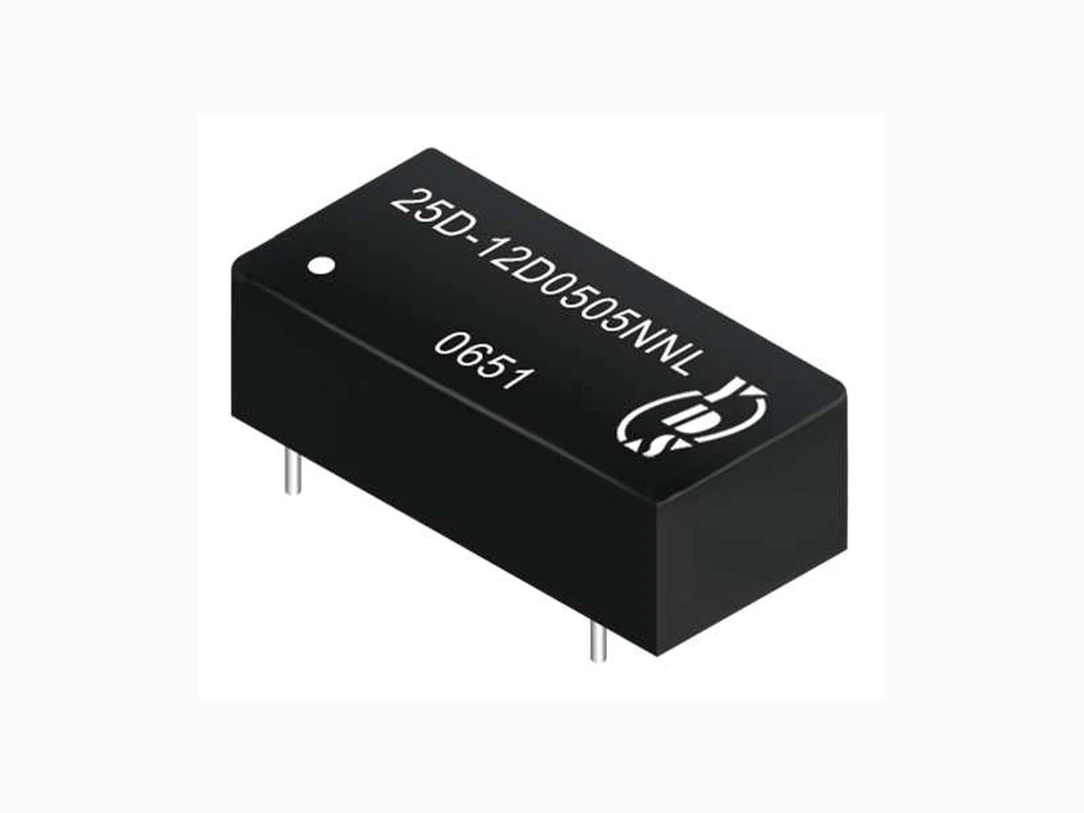
25D YUANDEAN
Document overview
- Manufacturer or author: Provided By www.digicamel.com(FREE DATASHEET DOWNLOAD SITE)
- PDF pages: 2
Technical content
FEATURES : High Efficiency up to 85% Internal SMD Construction Unregulated Output Types Operating Temperature:-40℃ TO +85℃ No External Component Required Industry Standard Pinout DC-DC Converter 25D SERIES 1Watt 1KV Isolated Twin Output DIL14 Specifications typical at TA=25°C, nominal input voltage and rated output current unless otherwise specified Part Number Output2 Efficiency Voltage (VDC) Current (mA) %Typ 25D-XXDXX03NNL 3.3 150 70 25D-XXDXX05NNL 5 100 75 25D-XXDXX09NNL 9 56 75 25D-XXDXX12NNL 12 42 75 25D-XXDXX15NNL 15 34 75 25D-XXDXX24N2NL 24 21 75 YUAN DEAN SCIENTIFIC YUAN DEAN SCIENTIFIC CO.,LTD Rev:1 2018/10/09 25D SERIES Temperature Derating Graph Input Specifications Parameters Conditions Min Typ Max Units Voltage Tolerance Vo,Io Nom ±5 % Filter Capacitor Output Specifications Parameters Conditions Min Typ Max Units Voltage Tolerance 100% full load ±5 % Short Circuit Protection Short Term 1 Sec Line Regulation For 1.0% OF Vin 1.2 % Load Regulation 3.3V,5V Load Regulation 9V,12V,15V,24V Ripple & Noise BW=DC To 20MHz 100 mVp-p Transient response setting time 50% load step change 350 us 100 OutPut Power(%) -40 85 100 Ambient Temperature( ℃) Nature Convection Note: 1.”XX” Is Voltage:03=3.3Vdc,05=5Vdc,09=9Vdc 12=12Vdc,15=15Vdc,24=24Vdc. 2. 3.3V for output only, not for input. The input voltage increases, there will be an increase in efficiency. 4. Over 24Vdc input voltage or Output voltage, using the 2nd package
Parameters Conditions Min Typ Max Units Isolation Resistance 500Vdc 1000 MΩ Switching Frequency Full load, nominal input 100 KHz Operating Temperature -40 +85 ℃ Humidity Non Condensing 95 % Cooling Free air Convection Case material DAP MTBF MIL-HDBK-217F @25℃ 3500000 Hours Weight 2.3 or 2.8 g Dimensions 20.32x10.16x6.80 mm Dimensions 20.32x10.16x7.70 mm 25D SERIES YUAN DEAN SCIENTIFIC CO.,LTD Rev:1 2018/10/09 Markings and dimensions PIN Connection PIN 1 7 8 9 10 11 14 Dual -Vin NC -Vout2 +Vout2 -Vout1 +Vout1 +Vin Recommended Test Circuit Part Number 25D - 12 D 0505 N NL A B C D E F A:Series B:Input Voltage C:Dual Output D:Output Voltage E:Unregulated(N) F:RoHS Version Unit :mm Unless otherwise specified, all tolerances are ±0.25 Tolerance Envelope Graph Output Current(%) Output Voltage(%) 120% 110% 100% 90% 80% 70% 10% 20% 30% 40% 50% 60% 70% 80% 90% 100% 110% 120% 1 7 14 10 9 8 TOP VIEW BOTTOM VIEW 20.32 10.16 0.50±0.05 7.62 7.62 15.24 4.00 6.80MAX 0.25±0.05 7.62 2.54 Dual Vin +Vout1 GND Cin Cout 5V :Cin 4.7uF,25V 9V:Cin 4.7uF,25V 12V:Cin 2.2uF,25V 15V:Cin 1uF,50V 24V:Cin 1uF,50V 3.3V :Cout 22uF,25V 5V :Cout 10uF,25V 9V :Cout 4.7uF,25V 12V:Cout 2.2uF,25V 15V:Cout 1uF,50V 24V:Cout 1uF,50V Cout -Vout1 +Vout2 -Vout2 Packaging Size(mm) A B C 13.23 12.30 530 1 7 14 11 9 8 TOP VIEW BOTTOM VIEW 20.32 10.16 4.00 7.62 0.50±0.05 7.62 7.62 15.24 0.25±0.05 7.70 2.54