

 Download PDF
IMX15 BEL
Document overview
- PDF pages: 19
Technical content
Page 1
Description
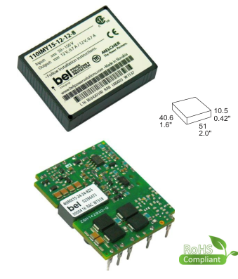
The IMX15, IMS15, and IMY15 Series of board mountable 15 Watt DC-DC converters have been designed according to the latest industry requirements and standards. The converters are particularly suitable for use in mobile or stationary applications in transport, railways, industry, or telecommunication, where variable input voltages or high transient voltages are prevalent. Covering a total input voltage range from 8.4 up to 150 V with different models, the converters are available with single and electrically-isolated double outputs from 3.3 up to 48 V, externally adjustable, with flexible load distribution on doubleoutput models. A shutdown input allows for remote on/off.
Features include efficient input and output filtering and consistently high efficiency over the entire input voltage range, high reliability, and excellent dynamic response to load and line changes. The converters have been approved by CSA. 20IMS/20IMX15 and 40IMS/40IMX15 models provide supplementary insulation. Connected to a secondary circuit, these models provide SELV
Table of Contents
Page
Description ............................................................................. 1 Model Selection ..................................................................... 2 Functional Description ........................................................... 4 Electrical Input Data ............................................................... 5 Electrical Output Data ............................................................ 8 Auxiliary Functions ............................................................... 13
Features
- RoHS lead-free-solder and lead-solder-exempted products are available.
- Wide input voltage ranges up to 150 VDC
- 1 or 2 isolated outputs up to 48 V
- 1500 to 3000 VAC I/O voltage withstand test
- Emissions EN 55022 level A
- Immunity to IEC/EN 61000-4-2,-3,-4,-5, and -6
- Fire&smoke as per EN 45545
- High efficiency (typ. 86%)
- Input undervoltage lockout
- Shutdown input, adjustable output voltages
- Flex power: Flexible load distribution on outputs
- Outputs no-load, overload, and short-circuit proof
- Operating ambient temperature –40 to 85 °C
- Thermal protection
- 2" x 1.6" case with 10.5 mm profile
- Supplementary insulation: 20/40IMX15 models, double or reinforced insulation: 110IMY15 models Safety-approved to IEC 60950-1 and UL/CSA 60950 -1 2nd Edition
1
1 110IMY15 models
outputs, even if the bus voltage at the converter input exceeds the SELV-limit of 60 VDC. The 110IMY15 models provide double insulation and are CE marked. They may be connected to a rectified 110 VAC source without any further isolation barrier. The circuitry is comprised of integrated planar magnetics. All components are automatically assembled and solidly soldered onto a single PCB without any wire connection. Magnetic feedback ensures maximum reliability and repeatability in the control loop over all operating conditions. Careful consideration of possible thermal stress ensures the absence of hot spots providing long life in environments, where temperature cycles are frequent. The thermal design allows
operation at full load up to an ambient temperature of 71 °C in free air without using any potting material. For extremely high vibration environments the case has holes for screw mounting.
Page
Electromagnetic Compatibility (EMC) .................................. 14 Immunity to Environmental Conditions ................................ 16 Mechanical Data .................................................................. 17 Safety and Installation Instructions ...................................... 18 Description of Options ......................................................... 19 Accessories.......................................................................... 19
Copyright © 2017, Bel Power Solutions Inc. All rights reserved.
Page 1 of 19
Page 2
Model Selection
Table 1: Model Selection
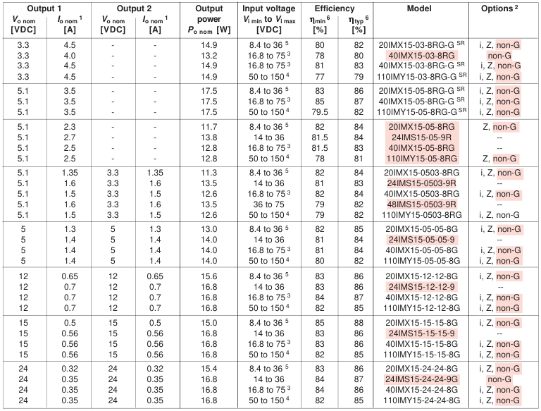
Flexible load distribution on dual and double outputs possible; up to 75% of the total output power Po nom on one of the 2 outputs. 1 IMX/IMY15-0503 models have reduced load distribution flexibility; 1.8 A max. on one of the 2 outputs. The total output power should not exceed Po nom. See Description of Options. 2 Short-time operation down to Vi = 14.4 V possible (Po reduced to approx. 85% of Po nom) 3 Short-time operation down to Vi = 43.2 V possible (Po reduced to approx. 85% of Po nom) and up to 154 V 4 Initial start-up at 9 V, main output voltage regulation down to 8.4 V 5 Efficiency at TA = 25 °C, Vi nom, Io nom. 6 SR Models with synchronos rectifier. For the RoHS version of such models, add -G !
Preferred for new designs. NFND Not for new designs. Replace 24IMS15 models by 20IMX15 and 48IMS15 by 40IMX15;
Replace 20IMX15-05, 40IMX15-05, 110IMY15-05 by models with synchronos rectifierSR; for new designs, chose always the RoHS version !
Page 2 of 19
Page 3
RoHS-Compliant Models The type designation of RoHS-compliant models (compliant for the restriction of all six substances) for the IMX/IMY15 Series ends with "G". However, in single-output models with 3.3 V or 5.1 V output an extra hyphen (-) is added after the existing "G", which already signifies a synchronous rectifierSR. This is an exception to our normal nomenclature to identify this type of product, since G is already used to designate products for higher output current fitted with a synchronous rectifier. Some examples – 20IMX15-05-8R-G designates a standard version with RoHS compliance for all six substances. – 20IMX15-05-8RG designates a synchronous rectifierSR version which is not RoHS-compliant.
– 20IMX15-05-8RG-G designates a synchronous rectifierSR version and RoHS compliant for all six substances. – 20IMX15-05-05-8G designates a double-output model with RoHS compliance for all six substances – 110IMY15-24-24-8RG designates a double-output model with RoHS compliance for all six substances.
Part Number Description
40 IMX15 - 05 -8 R G Z -G
xxix
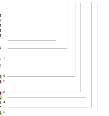
Input voltage range Vi
8.4 to 36 V ...................................................... 20 14 to 36 V ....................................................... 24 16.8 to 75 V .................................................... 40 36 to 75 V ....................................................... 48 50 to 150 V ................................................... 110
Series
IMX15, IMS15, IMY15
Output voltage of output 1............................03, 05, 12, 15, 24 Hyphen designating double-output models with two
electrically isolated outputs ...............................-
Output voltage of output 2............................03, 05, 12, 15, 24 Operating ambient temperature range TA
– 40 6 to 85 °C ..................................................-8 6 – 40to 71 °C.....................................................-9 2
Options and features:
R input and magnetic feedback....................... R Synchronous rectification ................................ G Inhibit ................................................................. i Open frame ......................................................Z RoHS-compliant for all 6 substances........ G or -G Not applicable to -0503 models. They have a common ground. 1 IMS15 models are not recommended for new designs. 2 Standard for single-output and -0503 models 3 Option i replaces the standard shutdown function; see Description of Options. 4 RoHS models with synchronous rectifier end as an exception with -G. 5 Only –25 °C for older -8RGSR models (Rev. < BA); see table 7a.
6
Note: The sequence of options must follow the order above !
Examples: 20 IMX15-05-05-8G: DC-DC converter, input 9 to 36 V, 2 galvanically isolated outputs each providing 5 V, 1.3 A,
RoHS-compliant 110IMY15-0503-8RG: DC-DC converter, input 50 to 150 V, 2 outputs with common return providing +5.1 V, 1.5 A and +3.3 V, 1.5 A, RoHS-compliant. Converter fitted with magnetic feedback for tight output voltage regulation.
Product Marking The converters without option Z are marked with basic type designation, input and output voltages and currents, applicable safety approval and recognition marks, patent nos., company logo, date code, and serial number.
Page 3 of 19
Page 4
Functional Description
The IMX15/IMS15/IMY15 Series of DC-DC converters are magnetic feedback-controlled flyback converters using current mode PWM (Pulse Width Modulation). The -05- and -0503- output voltage models exhibit an active magnetic feedback loop via a pulse transformer, resulting in very tight regulation of the output voltage (see the block diagrams). The output voltages of these models can be adjusted via the R-input. The R-input is referenced to the secondary side and allows for programming the output voltages in the range of approximately 80 to 105% of Vo nom, using either an external resistor or an external voltage source. Several single-output models with 3.3 or 5.1 V output exhibit a
synchronous rectifier to improve the efficiency. The voltage regulation on the double-output models is achieved with an auxiliary winding of the main transformer. The output voltages can be adjusted via the Trim input, which is referenced to the primary side and allows for programming the output voltage in the range of 100 to 105% of Vo nom via an external resistor, or within 75 to 105% if using an external voltage source. The load regulation output characteristic allows for paralleling of one or more double-output models with equal output voltage. Current limitation is provided by the primary circuit, thus limiting the total output power of double-output models. The shutdown
input allows remote converter on/off. Overtemperature protection will disable the converter under excessive overload conditions with automatic restart.
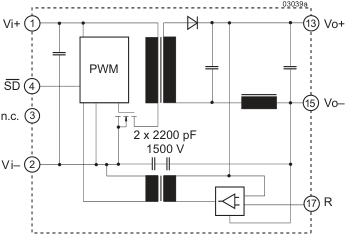
Fig. 1 Block diagram of single-output models
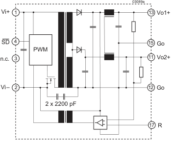
Fig. 2 Block diagram of -0503-models
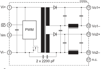
Fig. 3 Block diagram of double-output models
Page 4 of 19
Page 5
Electrical Input Data
General conditions: – TA = 25 °C, unless TC is specified. – Shut-down pin left open-circuit. – Trim or R input left open-circuit.
Table 2a: Input data of IMX15 and IMY15 models
| Input | 20IMX | 40IMX | 110IMY | Unit | |||
|---|---|---|---|---|---|---|---|
| Characteristics | Conditions | min typ max | min typ max | min typ max | |||
| V i | Input voltage range 1 | T – T A min A max I = 0 – I o o nom | 9 5, 7 36 | 16.8 5, 6 75 | 50 5 150 8 | V | |
| V i nom | Nominal input voltage | 20 | 40 | 110 | |||
| V i sur | Repetitive surge voltage | Abs. max input (3 s) | 40 | 100 | 168 | ||
| t startup | Converter start-up time 2 | Switch on | Worst case condition at V min, I = I i o o nom | 0.25 0.5 | 0.25 0.5 | 0.5 0.8 | s |
| SD high | 0.1 | 0.1 | 0.1 | ||||
| t rise | Rise time 2 | V , resistive load i nom | 5 | 5 | 5 | ms | |
| I , capac. load o nom | 10 20 | 10 20 | 10 20 | ||||
| I i o | No-load input current | I = 0, V – V o i min i max | 65 | 45 | 15 | mA | |
| I irr | Reflected ripple current | I = 0 – I o o nom | 30 | 30 | 20 | mA pp | |
| I inr p | Inrush peak current 3 | V = V i i nom | 8 | 9 | 10 | A | |
| C i | Input capacitance | for surge calculation | 1.5 | 0.75 | 0.35 | µF | |
| V–– SD | Shut-down voltage | Converter disabled | –10 to 0.7 | –10 to 0.7 | –10 to 0.7 | V | |
| Converter operating | open or 2 – 20 | open or 2 – 20 | open or 2 – 20 | ||||
| R–– SD | Shut-down input resistance | approx. 10 | approx. 10 | approx. 10 | kΩ | ||
| I–– SD | Input current, when disabled | V – V i min i max SD connected to Vi– | 10 | 3 | 1 | mA | |
| f s | Switching frequency | V – V , i min i max I = 0 – I o o nom | approx. 300 | approx. 300 | approx. 300 | kHz | |
| V i RFI | Input RFI level conducted | EN 55032 4 | A | A | A | ||
If Vo is set above Vo nom by use of the R or Trim input, Vi min will be proportionately increased. 1 Measured with resistive and max. admissible capacitive load. Valid for models with rev. AI or greater. 2 Source impedance according to ETS 300132-2, version 4.3. 3 Measured with a ceramic capacitor Ci directly across input; output lead length 0.1 m, leads twisted. Double-output models with both 4 outputs in parallel. Ci is specified in table 11. Input undervoltage lockout at typ. 80% of Vi min. 5 Short time operation down to Vi min >14.4 V possible. Po reduced to approx. 85% of Po nom. 6 Initial start-up at Vi = 9 V, main output voltage regulation down to 8.4 V
7 Short time operation up to 154 V possible for 2 s. 8
Page 5 of 19
Page 6
Table 2b: Input Data of IMS15 models; general conditions as in table 2a
| Input | 24IMS | 48IMS | Unit | |||
|---|---|---|---|---|---|---|
| Characteristics | Conditions | min typ max | min typ max | |||
| V i | Input voltage range 1 | T – T A min A max I = 0 – I o o nom | 14 36 | 36 75 | V | |
| V i nom | Nominal input voltage | 24 | 48 | |||
| V i sur | Repetitive surge voltage | Abs. max input (3 s) | 50 | 100 | ||
| t startup | Converter start-up time 2 | Switch on | Worst case condition at V min, I = I i o o nom | 0.25 0.5 | 0.25 0.5 | s |
| SD high | 0.1 | 0.1 | ||||
| t rise | Rise time 2 | V , resistive load i nom | 5 | 5 | ms | |
| I , capac. load o nom | 10 20 | 10 20 | ||||
| I i o | No-load input current | I = 0, V – V o i min i max | 20 40 | 10 20 | mA | |
| I irr | Reflected ripple current | I = 0 – I o o nom | 30 | 30 | mA pp | |
| I inr p | Inrush peak current 3 | V = V i i nom | 5 | 4.5 | A | |
| C i | Input capacitance | for surge calculation | 4 | 2 | µF | |
| V–– SD | Shut-down voltage | Converter disabled | –10 to 0.7 | –10 to 0.7 | V | |
| Converter operating | open or 2 – 20 | open or 2 – 20 | ||||
| R–– SD | Shut-down input resistance | approx. 10 | approx. 10 | kΩ | ||
| I–– SD | Input current, when disabled | V – V i min i max SD connected to Vi– | 1.2 3 | 1.2 3 | mA | |
| f s | Switching frequency | V – V , i min i max I = 0 – I o o nom | approx. 300 | approx. 300 | kHz | |
| V i RFI | Input RFI level conducted | EN 55022 4 | A | A | ||
If Vo is set above Vo nom by use of the R or Trim input, Vi min will be proportionately increased. 1 Measured with resistive and max. admissible capacitive load. 2 Source impedance according to ETS 300132-2, version 4.3. 3 Measured with a ceramic capacitor Ci directly across input; output lead length 0.1 m, leads twisted. Double-output models with both 4 outputs in parallel. Ci is specified in table 11. Input undervoltage lockout at typ. 80% of Vi min. 5
Page 6 of 19
Page 7
Inrush Current The inrush current has been made as low as possible by choosing a very small input capacitance. A series resistor may be installed in the input line to further reduce this current.
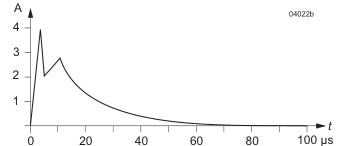
Fig. 4 Typical inrush current at Vi nom, Po nom versus time (40IMX15). Source impedance according to ETS 300132-2 at Vi nom.
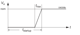
Vo nom
Fig. 5 Converter start-up and rise time
Input Undervoltage Lockout A special feature of these converters is the accurate undervoltage lockout protection, which protects against large currents caused by operation at low voltages. This ensures easier start-up in distributed power systems.
Tab. 3: Turn on and turn off voltage
| Model | Turn on | Turn off | Unit |
|---|---|---|---|
| min max | min max | ||
| 20IMX15 | 7.5 8 | 7 7.5 | V |
| 24IMS15 | 12.5 13.5 | 12 13 | |
| 40IMX15 | 12.5 13.5 | 12 13 | |
| 48IMS15 | 31.5 32.5 | 31 32 | |
| 110IMY15 | 40 42.5 | 38 40.5 |
Fuse and Reverse Polarity Protection The built-in suppressor diode also provides for reverse polarity protection at the input by conducting current in the reverse direction. An external fuse is required to limit this current. Table 4: Recommended external fuses
| Model | Fuse type |
|---|---|
| 20IMX15 | F 4.0 A |
| 24IMS15 | F 3.15 A |
| 40IMX15, 48IMS15 | F 2.0 A |
| 110IMY15 | F 1.0 A |
Input Transient Voltage Protection A built-in suppressor diode provides effective protection against input transients, which typically occur in many installations. Table 5: Built-in transient voltage suppressor
| Type | Breakdown voltage V [V] Br nom | Peak power at 1 ms P [W] p | Peak pulse current I [A] pp |
|---|---|---|---|
| 20IMX15 | 40 | 1500 | 22 |
| 24IMS15 | 53 | 600 | 7.7 |
| 40IMX15 | 100 | 1500 | 9.7 |
| 48IMS15 | 100 | 600 | 4.1 |
| 110IMY15 | 168 | 600 | 0.5 |
For very high energy transients as for example to achieve compliance to IEC/EN 61000-4-5 (see table Electromagnetic Immunity), an external inductor and a capacitor are required, see Fig. 6. The components are specified in table 6.
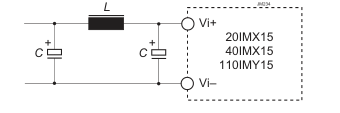
Fig. 6 Example for external circuitry to achieve better transient immunity. Values of components in the table below.
Table 6: Components for external circuitry for IEC/EN 61000-4-5, level 3 compliance.
| Model | Inductor (L) | Capacitor (C) |
| 20IMX15 | 220 µH, 2.7 A | 2 x 330 µF, 63 V |
| 24IMS15 | 220 µH, 1.3 A | 2 x 330 µF, 63 V |
| 40IMX15 | 220 µH, 1.3 A | 2 x 330 µF, 100 V |
| 48IMS15 | 220 µH, 1 A | 2 x 330 µF, 100 V |
| 110IMY15 | 220 µH, 0.4 A | 2 x 330 µF, 200 V |
Page 7 of 19
Page 8
Electrical Output Data
We recommend connecting an external 1 µF ceramic capacitor across the output pins. General conditions: – TA = 25 °C, unless TC is specified – Shutdown pin and Trim or R pin left open-circuit (not connected)
Table 7a: Output data for single-output models -03-8RG 1 and 05-8RG 1
| Output | 3.3 V | 5.1 V | Unit | |||
|---|---|---|---|---|---|---|
| Characteristics | Conditions | min typ max | min typ max | |||
| V o | Output voltage | V i nom I = 0.5 I o o nom | 3.25 3.35 | 5.05 5.15 | V | |
| I o nom | Output current 20IMX 40IMX /110IMY | V to V i min i max | 4.5 | 3.5 | A | |
| 4.5 | 3.5 | |||||
| I o L | Current limit 2 | V , T = 25 °C i nom C V ≤ 93% V o o nom | 6.0 | 4.6 | ||
| ∆V o | Line/load regulation | V to V , i min i max (0.1 to 1) I o nom | ±0.5 | ±0.5 | % | |
| V o | Output voltage noise | V to V 4 i min i max I = I o o nom 5 | 100 | 100 | mV pp | |
| 60 | 60 | |||||
| V o L | Output overvoltage limit. 3 | 115 130 | 115 130 | % | ||
| C o ext | Admissible capacitive load | 0 4000 6 | 0 4000 6 | µF | ||
| V o d | Dynamic load regulation | Voltage deviat. | V i nom I ↔ 1/2 I o nom o nom IEC/EN 61204 | ±250 | ±250 | mV |
| t o d | Recovery time | 1 | 1 | ms | ||
| α Vo | Temperature coefficient ∆V /∆T o C | V to V i min i max (0.1 to 1) I o nom | ±0.02 | ±0.02 | %/K | |
SR Models -8RG (synchr. rectifier) have a minimum case and operating temperature of –25 °C. If the revision is BA (or later), it is –40 °C. 1 The current limit is primary side controlled. In the event of a sustained overload condition the thermal protection may cause the converter 2 to shut down (restart after cooling down). The overvoltage protection is via a primary side second regulation loop. It is not tracking with R control. 3 BW = 20 MHz 4 Measured with a probe according to EN 61204 5 Co ext is limited to 3000 µF, if Vi >125 V or TA < 25 °C 6
Page 8 of 19
Page 9
Table 7b: Output data for -05-8R and -0503-8R models; general conditions as in table 7a
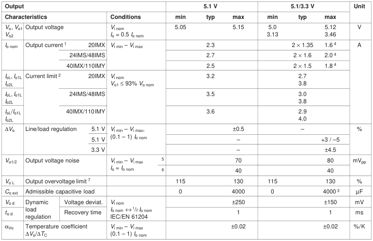
Flexible load distribution: Io max for one of the 2 outputs; however the total load should not exceed Po nom specified in the table Model 1 Selection. The current limit is primary-side controlled. 2 For -0503-models: total capacitive load of both outputs. 3 For -0503-models: Conditions for specified output. Other output loaded with constant current Io = 0.5 Io nom. 4 BW = 20 MHz 5 Measured with a probe according to EN 61204 6 The overvoltage protection is via a primary side second regulation loop. It is not tracking with R control. 7
Page 9 of 19
Page 10
able 7c: Output data for double-output models; general conditions as in table 7a
| Output | 2 ××××× 5 V | 2 ××××× 12 V | 2 ××××× 15 V | 2 ××××× 24 V | Unit | |||
|---|---|---|---|---|---|---|---|---|
| Characteristics | Conditions | min typ max | min typ max | min typ max | min typ max | |||
| V o1 | Output 1 24IMS/48IMS other models | V i nom I = 0.5 I o o nom | 4.95 5.05 | 11.88 12.12 | 14.85 15.15 | 23.70 24.30 | V | |
| 4.95 5.05 | 11.90 12.10 | 14.88 15.12 | 23.80 24.20 | |||||
| V o2 | Output 2 24IMS/48IMS other models | 4.94 5.06 | 11.84 12.16 | 14.80 15.20 | 23.64 24.36 | |||
| 4.94 5.06 | 11.88 12.12 | 14.85 15.15 | 23.75 24.25 | |||||
| I o nom | Output current 1 20IMX other models | V – V i min i max | 2 ××××× 1.3 | 2 ××××× 0.65 | 2 ××××× 0.50 | 2 ××××× 0.32 | A | |
| 2 ××××× 1.4 | 2 ××××× 0.70 | 2 ××××× 0.56 | 2 ××××× 0.35 | |||||
| I oL | Current limit 2, 4 20IMX 24IMS/48IMS 40IMX/110IMY | V i nom V ≤ 93% V o1 o nom | 3.0 | 1.6 | 1.3 | 0.85 | ||
| 3.5 | 1.9 | 1.6 | 0.95 | |||||
| 3.2 | 1.7 | 1.4 | 0.90 | |||||
| ∆V o1 | Line/load regulation 8 output 1 output 2 | V – V , I i min i max o nom | ±1 | ±1 | ±1 | ±1 | % | |
| ∆V o2 | V , (0.1 – 1) I i nom o nom | ±3 | ±3 | ±3 | ±3 | |||
| V o1/2 | Output voltage noise | V – V 5 i min i max I = I o o nom 6 | 80 | 120 | 150 | 240 | mV pp | |
| 40 | 60 | 70 | 120 | |||||
| V o L | Output overvoltage limit 7 8 | Min. load 1% | 115 130 | 115 130 | 115 130 | 115 130 | % | |
| C o ext | Admissible capacitive load 3 | 0 4000 | 0 680 | 0 470 | 0 180 | µF | ||
| V o d | Dynamic load regulation | Voltage deviat. | V i nom I ↔ 1/2 I o nom o nom | ±250 | ±300 | ±300 | ±600 | mV |
| t o d | Recovery time | 1 | 1 | 1 | 1 | ms | ||
| α Vo | Temperature coefficient ∆V /∆T o C | V – V i min i max (0.1 – 1) I o nom | ±0.02 | ±0.02 | ±0.02 | ±0.02 | %/K | |
Flexible load distribution: Each output of double-output models is capable of delivering 75% of the total output power; however the total 1 load should not exceed Po nom specified in the table Model Selection. The current limit is primary-side controlled. 2 Measured with both outputs connected in parallel. 3 Conditions for specified output. Other output loaded with constant current Io = 0.5 Io nom. 4 BW = 20 MHz 5 Measured with a probe according to EN 61204 6 The overvoltage protection is via a primary side second regulation loop, not tracking with Trim or R control. 7 At start-up occurs a short overshoot at the output. 8
Page 10 of 19
Page 11
Thermal Considerations If a converter, mounted on a PCB, is located in free, quasistationary air (convection cooling) at the indicated maximum
TA max (see table Temperature
ambient temperature specifications) and is operated at its nominal input voltage and output power, the case temperature measured at the measuring point of case temperature TC (see Mechanical Data) will approach the indicated value TC max after the warmup phase. However, the relationship between TA and TC depends heavily on the conditions of operation and integration into a system. The thermal conditions are influenced by input voltage, output current, airflow, temperature of surrounding components and surfaces, and the properties of the printed circuit board. TA max is therefore only an indicative value. Caution: The case temperature TC measured at the measuring
point of case temperature TC (see Mechanical Data) may under no circumstances exceed the specified maximum value. The installer must ensure that under all operating conditions TC remains within the limits stated in the table Temperature specifications.
Po/Po max
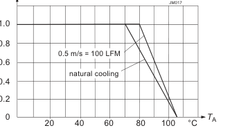
Fig. 7 Maximum output power versus ambient temperature
Overtemperature Protection The converters are protected from possible overheating by means of an internal temperature monitoring circuit. It shuts down the converter above the internal temperature limit, and attempts to automatically restart in short intervals. This feature helps protect against excessive internal temperatures, which could occur during heavy overload conditions.
Output Overvoltage Protection The output of single-output models as well as -0503- and -05- 05-models are protected against overvoltage by a second control loop. In the event of an overvoltage on one of the outputs, the converter will shut down and attempt to restart in short intervals. Doubel-output models (except -0503- and -05-05-models) are protected against overvoltage by a Zener diode across the second output. Under worst case conditions the Zener diode will become a short circuit. Since with double-output models both outputs track each other, the protection diode is only provided in one of the outputs. The main purpose of this feature is to protect against possible overvoltage, which could
occur due to a failure in the control logic. This protection circuit is not designed to withstand externally applied overvoltages.
Short Circuit Behavior The current limit characteristic shuts down the converter, whenever a short circuit is applied to its output. It acts selfprotecting, and automatically recovers after removal of the overload condition (hiccup mode).
Parallel and Series Connection The outputs of one or several single- or double-output models
Vo [%]
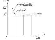
Fig. 8 Overload switch-off (hiccup mode); typical values
can be connected in series without any precautions, taking into consideration that the highest output voltage should remain below 42 V to ensure that the output remains SELV. Both outputs of the same converter with equal voltage (e.g. 5 V / 5 V) can be connected in parallel and will share their output currents equally. Parallel operation of single or double outputs of two or more converters with the same output voltage may cause start-up problems at initial start-up. This is only advisable in applications, where one converter is able to deliver the full load current as, for example, required in true redundant systems. Note: If the 2nd output of double-output models (except 0503) is not
used, connect it in parallel to the 1st output.
Typical Performance Curves General conditions: – TA = 25 ºC, unless TC is specified. – Shutdown pin left open-circuit. – Trim or R input not connected.
0 0.4 0.8 1.2 1.6 2.0 2.4 2.8 3.2 3.6 4 A
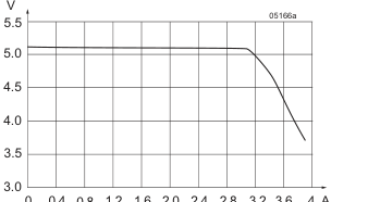
Fig. 9 Vo versus Io (typ) of converters with Vo = 5.1 V (110IMY15-05-8R)
Page 11 of 19
Page 12
V
0 0.2 0.4 0.6 0.8 1.0 1.2 1.4 1.6 1.8 A
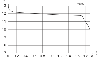
Fig. 10 Vo versus Io (typ.) of double-output models (2 x 12 V), with both outputs in parallel (110IMY15-12-12-8)
V
0.5 0.6 0.7 A
0.3 0.4
0.1 0.2
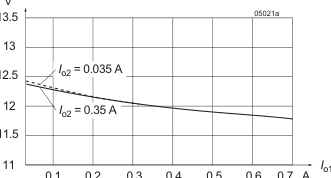
Fig. 11 Cross load regulation Vo1 versus Io1 (typ.) for various Io2 (2 x 12 V).
%
1 Po/Po nom
0.25
0.5
0.75
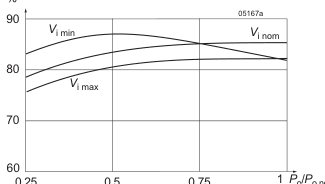
Fig. 12a Efficiency versus input voltage and load. Typical values (40IMX15-12-12-8).
%
1 Po/Po nom
0.25
0.5
0.75
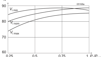
Fig. 12b Efficiency versus input voltage and load. Typical values (110IMY15-12-12-8)
%
1 Io1/Io1 nom
0.5
0.75
0.25
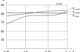
Fig. 12c Efficiency versus input voltage and load. Typical values (48IMS15-12-12-9)
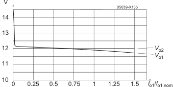
Fig. 13 Flexible load distribution on double-outputs models with option R (110IMY15-12-12-8R): Load variation from 0 to 150% of Io1 nom on output 1; output 2 loaded with 50% of Io2 nom.
Page 12 of 19
Page 13
Auxiliary Functions
Shutdown Function The outputs of the converters may be enabled or disabled by means of a logic signal (TTL, CMOS, etc.) applied to the shutdown pin. If this function is not required, the shut-down pin should be left open-circuit.
- Converter operating:
2.0 to 20 V
- Converter disabled:
–10 to +0.7 V
Adjustable Output Voltage
- R input for single-output models and -0503-models
- Trim input for double-output models
As a standard feature, the single- and double-output models offer adjustable output voltage(s) by using the control input R or Trim. If the control input is left open-circuit, the output voltage is set to Vo nom. For output voltages Vo > Vo nom, the minimum input voltage Vi min (see Electrical Input Data) increases
proportionally to Vo/Vo nom. Single-output models with synchronous rectifier (G): The R input is referenced to the secondary side of the converter. Adjustment of the output voltage is possible by means of an external resistor connected between the R pin and either Vo+ or Vo–. Note: For models with synchronous rectifier the logic for Vo adjustment differs from other models with R input.
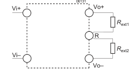
Fig. 14 Output voltage control for single-output models with synchronous rectifier.
Table 8: Vo versus Vext approximate values
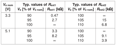
All other models fitted with R-input: The R input is referenced to the secondary side of the converter. Adjustment of the output voltage is possible by means of either an external resistor or a voltage source.
a) Adjustment by means of an external resistor Rext. Depending upon the value of the required output voltage, the resistor shall be connected: either: Between the R pin and Vo– to achieve an output voltage adjustment range of Vo ≈ 80 to 100 % of Vo nom. Vo Rext1 ≈ 4 kΩ • ––––––––– Vo nom – Vo or: Between the R pin and Vo+ to achieve an output voltage range of Vo ≈ 100 to 105% of Vo nom.
(Vo – 2.5V) Rext2 ≈ 4 kΩ • –––––––––––––––––– 2.5 V • (Vo/Vo nom – 1) b) Adjustment by means of an external voltage Vext between Vo– and R pin. The control voltage range is 1.96 to 2.62 V and allows for adjustment in the range of Vo ≈ 80 to 105% of Vo nom. Vo • 2.5 V Vext ≈ –––––––– Vo nom Attempting to adjust the output below this range will cause the converter to shut down (hiccup mode). Note: Applying an external control voltage >2.75 V may damage the converter.
06029e
| Vi+ Vi– | V = 2.5 V 4 kΩ ref + Control logic | Vo+ R ext2 R + R ext1 – Vo– |
Vext
Fig. 15 Output voltage control for single-output models, -0503-models, and double-output models by means of the R input.
Double-output models with Trim input: The Trim input is referenced to the primary side. The figure below shows the topology. Adjustment is possible trough either an external resistor or an external voltage source Vext.
06089a
| Vi+ Trim R ext Vi– | Control circuit V 2.5 V ref | Vo1+ |
| Vo1– Vo2+ Vo2– |
+ Vext –
Fig. 16 Output voltage control for double-output models (with Trim input) by means of the Trim input.
Page 13 of 19
Page 14
a) Adjustment by means of an external resistor Rext: Programming of the output voltage by means of an external resistor Rext is possible within 100 to 105% of Vo nom. Rext should be connected between the Trim pin and Vi–. Connection of Rext to Vi+ may damage the converter. The table below indicates suitable resistor values for typical output voltages under nominal conditions (Vi nom, Io = 0.5 Io nom) with either parallel-connected outputs or equal-load conditions on both outputs. Table 9a: Rext for Vo > Vo nom; approximate values (Vi nom, Io1, 2 = 0.5 Io1/2 nom )
| V [% V ] o o nom | R ext [kΩΩΩΩΩ] |
| 105 to 108 (107 typically) 105 104 103 102 101 100 | 0 1.5 5.6 12 27 68 ∞ |
Electromagnetic Compatibility (EMC)
A suppressor diode together with an input filter forms an effective protection against high input transient voltages, which
Electromagnetic Immunity
Table 10: Immunity type tests
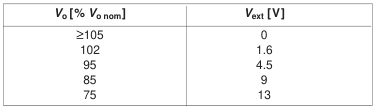
b) Adjustment by an external voltage source Vext: For programming the output voltage in the range 75 to 105% of Vo nom, a source Vext (0 to 20 V) is required, connected between the Trim pin and Vi–. The table below indicates values Vo versus Vext (nominal conditions Vi nom, Io = 0.5 Io nom), with either parallel-connected outputs or equal load conditions on both outputs. Applying a control voltage >20 V will set the converter into a hiccup mode. Direct paralleling of the Trim pins of parallel connected converters is possible.
Table 9b: Vo versus Vext for Vo = 75 to 105% Vo nom; typical values (Vi nom, Io1/2 = 0.5 Io1/2 nom)
typically occur in many installations, but especially in batterydriven mobile applications.
| Phenomenon | Standard | Class Level | Coupling mode 2 | Value applied | Waveform | Source Imped. | Test procedure | In oper. | Perf. crit. 3 |
| Electrostatic discharge to case | IEC/EN 61000-4-2 | 2 | contact discharge (R pin open) | 4000 V p | 1/50 ns | 330 Ω 150 pF | 10 positive and 10 negative discharges | yes | B |
| 3 | air discharge (R pin open) | 8000 V p | |||||||
| Electromagnetic field | IEC/EN 61000-4-3 | x 5 3 6 | antenna | 20 V/m 5 3 V/m 6 | AM 80% 1 kHz | n.a. | 80 to 1000 MHz | yes | A |
| ENV 50204 | 3 | antenna | 10 V/m | PM, 50% duty cycle, 200 Hz repetition frequ. | n.a. | 900 MHz | yes | A | |
| Electrical fast transients/burst | IEC/EN 61000-4-4 | 3 4 | direct +i/–i | 2000 V 4 p | bursts of 5/50 ns 5 kHz rep. rate transients with 15 ms burst duration and a 300 ms period | 50 Ω | 60 s positive 60 s negative transients per coupling mode | yes | A |
| Surges | IEC/EN 61000-4-5 | 2 3 1 | +i/–i | 1000 V p 2000 V 1 p | 1.2/50 µs | 2 Ω 18 µF | 5 pos. and 5 neg. surges | yes | B |
| RF conducted immunity | IEC/EN 61000-4-6 | 3 2 6 | +i/–i | 10 VAC 3 VAC 6 | AM modulated 80%, 1 kHz | 150 Ω | 0.15 to 80 MHz | yes | A |
External components required; see Fig. 6 and table 6. 1 i = input, o = output. 2 A = normal operation, no deviation from specs., B = temporary deviation from specs. possible. 3 Corresponds to the railway standard EN 50121-3-2:2006, table 9.3. Corresponds to the railway standard EN 50121-3-2:2006, table 9.1. Valid for 24IMS15 and 48IMS15
Page 14 of 19
Page 15
Conducted Emissions
PMM 8000 PLUS Date: 24.04.06 Time: 16:23
dbµV
Name: 20d12_1
20IMX15-12-12-8 Peak
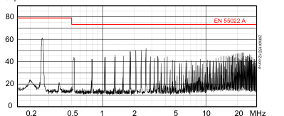
Fig. 17a Typ. disturbance voltage (peak) at pos. input according to EN 55011/032, measured at Vi nom and Io nom. Output leads 0.1 m, twisted, input capacitors see table 11 (20IMX15-12-12-8)
Date: 24.04.06 Time: 15:2 PMM 8000 PLUS Name: 40d12_1 40IMX15-12-12-8 Peak
dbµV
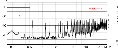
Fig. 17b Typ. disturbance voltage (peak) at pos. input according to EN 55011/032, measured at Vi nom and Io nom. Output leads 0.1 m, twisted, input capacitors see table 11 (40IMX15-12-12-8)
Date: 25.04.06 Time: 08:07 PMM 8000 PLUS
dbµV
Peak
Name: 110d12_1 110IMY15-12-12-9
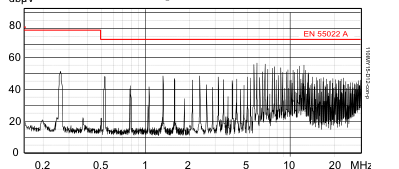
Fig. 17c Typ. disturbance voltage (peak) at pos. input according to EN 55011/032, measured at Vi nom and Io nom. Output leads 0.1 m, twisted, input capacitors see table 11 (110IMY15-12-12-8)
Table 11: External capacitors across the input to comply with EN 55011/EN 55032, Class A, conducted; see fig. 17.
| Model Ceramic | ML Electrolytic capacitor |
| 20IMX15, 24IMS15 0.47 µF/50 40IMX15, 48IMS15 0.33 µF/10 110IMY15 0.15 µF/20 | V 220 µF/50 V 0 V 220 µF/100 V 0 V 4.7 µF/200 V |
Date: 02.05.06 Time: 09:58 PMM 8000 PLUS
dbµV
Name: 40d12_4 40IMX15-12-12-8-Peak
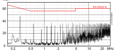
Fig. 18 Typ. disturbance voltage (peak) at input according to EN 55011/022, measured at Vi nom and Io nom. Output leads 0.1 m, twisted, input filter as in fig. 19 (40IMX15-12-12-8)
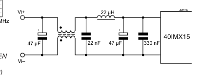
Fig. 19 Example for external circuitry to comply with EN 55011/ EN 55032, Class B, conducted. This filter was designed for a 40IMX15-12-12-8. All capacitors are rated to 100 V, the chokes to 1.5 A.
Page 15 of 19
Page 16
Immunity to Environmental Conditions
Table 12: Mechanical and climatic stress
| Test Method | Standard | Test Conditions | Status | |
|---|---|---|---|---|
| Cab | Damp heat steady state | IEC/EN 60068-2-78 MIL-STD-810D sect. 507.2 | Temperature: 40 ±2 C Relative humidity: 93 +2/-3 % Duration: 56 days | Converter not operating |
| Ea | Shock (half-sinusoidal) | IEC/EN 60068-2-27 MIL-STD-810D sect. 516.3 | Acceleration amplitude: 50 g = 490 m/s2 n Bump duration: 11 ms Number of bumps: 18 (3 each direction) | Converter operating |
| Fc | Vibration (sinusoidal) | IEC/EN 60068-2-6 | Acceleration amplitude: 0.35 mm (10 to 60 Hz) 5 g = 49 m/s2 (60 to 2000 Hz) n Frequency (1 Oct/min): 10 to 2000 Hz Test duration: 7.5 h (2.5 h each axis) | Converter operating |
| Fda | Random vibration wide band reproducibility high | IEC/EN 60068-2-35 | Acceleration spectral density: 0.05 g 2/Hz n Frequency band: 20 to 500 Hz Acceleration magnitude: 4.9 g n rms Test duration: 3 h (1 h each axis) | Converter operating |
| -- | Salt mist test sodium chloride (NaCl) solution | EN 50155:2007, clause 12.2.10 class ST2 | Temperature: 35 ±2 °C Duration: 16 h | Converter not operating |
Temperatures
Table 14: Temperature specifications Valid for air pressure of 800 to 1200 hPa (800 to 1200 mbar)
| Temperature | -9 | -8 | Unit | ||
|---|---|---|---|---|---|
| Characteristics | Conditions | min max | min max | ||
| T A | Ambient temperature | Operational 1 | –40 71 | –40 2, 3 85 | °C |
| T C | Case temperature | –40 95 | –40 2, 3 105 | ||
| T S | Storage temperature | Non operational | –55 85 | –55 85 | |
See Thermal Considerations 1 Start-up at –55 °C, except models with synchronous rectifier SR 2 –25 °C for all models with synchronous rectifier SR with Revision < BA. 3
Reliability
Table 13: MTBF
| Model | Standard | Ground Benign | Ground Fixed | Ground Mobile | Unit | |
|---|---|---|---|---|---|---|
| T = 40 °C C | T = 40 °C C | T = 70 °C C | T = 50 °C C | |||
| 20IMX15-12-12-8 | MIL-HDBK-217F | 697 000 | 366 000 | 229 000 | 312 000 | h |
| 20IMX15-15-15-8 | Belcore | 2 345 000 | 1 172 000 | 632 000 | 317 000 | |
| 48IMS15-05-05-9 | MIL-HDBK-217F | 535 000 | 283 000 | 179 000 | 245 000 | |
| 110IMY15-05-8R | MIL-HDBK-217F | 485 000 | 255 000 | 167 000 | 223 000 | |
| Belcore | 1 547 000 | 774 000 | 394 000 | 206 000 | ||
Page 16 of 19
Page 17
Mechanical Data
Dimensions in mm (inches). Tolerances ±0.3 mm, unless otherwise noted.
European Projection
Measuring point of case temperature TC
0.8 (0.03")
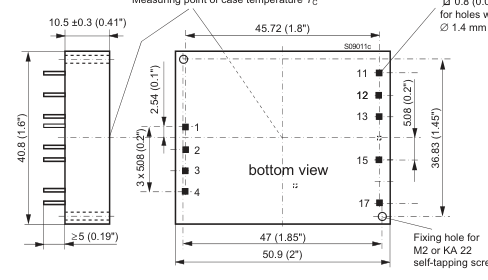
Fig. 20
Case IMX15, IMS15, IMY15
Material: Fortron 1140L6
Weight: <35 g
0.8 (0.03")
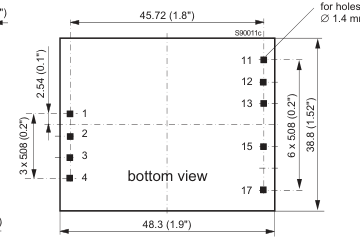
8.9 ±0.3 (0.35")
≥5 (0.19")
Fig. 21
Open frame (option Z)
for holes with
Page 17 of 19
Page 18
Safety and Installation Instructions
Pin allocation Table 15: Pin allocation
| Pin | Standard and Option Z single double -0503- | ||
| 1 | Vi+ | Vi+ | Vi+ |
| 2 | Vi– | Vi– | Vi– |
| 3 | - | Trim | n.c. |
| 4 | SD | SD | SD |
| 5 | - | - | - |
| 6 | - | - | - |
| 11 | - | Vo1+ | Vo2+ |
| 12 | - | Vo1– | Go |
| 13 | Vo+ | Vo2+ | Vo1+ |
| 15 | Vo– | Vo2– | Go |
| 17 | R | n.c. | R |
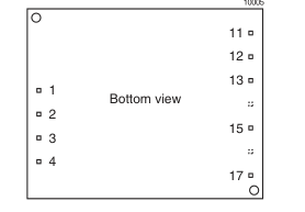
Fig. 22 Footprint
Installation Instructions Installation must strictly follow the national safety regulations in compliance with the enclosure, mounting, creepage, clearance, casualty, markings and segregation requirements of the end-use application. The converter must be connected to a secondary circuit. Do not open the converter. Ensure that a converter failure (e.g., by an internal short-circuit) does not result in a hazardous condition.
Input Fuse To prevent excessive current flowing through the input supply lines in case of a malfunction an external fuse should be installed in a non-earthed input supply line; see table 4.
Standards and Approvals The converters are approved according to IEC 60950-1 and UL/ CSA 60950-1 2nd Edition. 110IMY models are fitted with a CE mark.
The converters have been evaluated for:
- Building in
- Supplementary insulation input to output, based on their maximum input voltage (IMX15, IMS15)
- Reinforced insulation input to output, based on their maximum input voltage (IMY15 models)
- Pollution degree 2 environment (not option Z)
- Connecting the input to a secondary circuit subject to a maximum transient rating of 1500 V (IMX15, IMS15)
- Connecting the input to a secondary circuit subject to a maximum transient rating of 2500 V (IMY15)
The converters are subject to manufacturing surveillance in accordance with the above mentioned UL standards and with ISO9001:2008.
Railway Applications To comply with railway standards, all components are coated with a protective lacquer (except option Z).
Protection Degree and Cleaning Liquids The protection degree of the converters is IP 40, except openframe models (option Z). In order to avoid possible damage, any penetration of cleaning fluids should be prevented, since the power supplies are not hermetical sealed. However, open-frame models (option Z) leave the factory unlacquered; they may be lacquered by the customer, for instance together with the mother board. Cleaning liquids are not permitted – except washing at room temperature with isopropyl alcohol. If necessary, the mother board must be cleaned, before fitting the open-frame converter. Note: Cleaning liquids may damage the adhesive joints of the
ferrite cores.
Isolation The electric strength test is performed in the factory as routine test in accordance with EN 50514 and IEC/EN 60950. The Company will not honor any warranty claims resulting from incorrectly executed electric strength field tests.
Table 16: Electric strength test voltages
| Characteristic IMS15 | Input to output Out IMX15 IMY15 output | put toUnit | |||
|---|---|---|---|---|---|
| Factory test ≥1 s Equivalent DC voltage | 1.2 | 1.51 | 3.0 | 0.1 | kVAC |
| (1.7) | (2.1) | (4.2) | 0.15 | kVDC | |
| Insulation resistance at 500 VDC | >100 | >100 | >100 | - | MΩ |
| Partial discharge extinction voltage | Consult the Company | - | kV | ||
1 1.5 kVAC according to IEC 60950, sect. 6.2, Telecom equipment; type test with 1.5 kVAC / 60 s (IEE 802.3). IMX15 units produced before 2013 were tested only with 1.2 kVAC. 2 The test voltage between outputs is not applied as routine test.
Page 18 of 19
Page 19
Description of Options
Table 17: Survey of options
| Option | Function of option | Characteristic |
| -9 | Temperature range, NFND | See table Temperatures specifications |
| i | Inhibit | Replaces the shutdown function with inverted logic |
| Z | Open frame | See Mechanical Data |
Option -9 versus -8 IMX15 and IMY15 models with -9 (not for new designs) have a limited temperature range. Standard models with suffix -8 are rated up to TA = 85 °C; see table Temperature specifications.
Option i: Inhibit Replaces the shut-down function with inverted logic. The output(s) of the converter may be enabled or disabled by
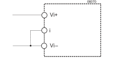
Fig. 23 If the inhibit function is not used, the inhibit pin should be connected to Vi–.
Accessories
Supports are available for chassis mounting CMBIMX15 (HZZ00626) and for DIN-rail mounting DMBIMX15 (HZZ00625). They exhibit the connectors and allow for placing different external components. For details see our Mounting Supports Data Sheet BCD20007 on our website.
means of a logic signal (TTL, CMOS, etc.) applied to the inhibit pin. No output voltage overshoot will occur, when the converter is turned on. If the inhibit function is not required, the inhibit pin should be connected to Vi– to enable the output (active low logic, fail safe). Voltage on pin i: Converter operating:
–10 V to 0.8 V 2.4 V to Vi max (<75 V) or
Converter inhibited:
pin i left open-circuit.
Option Z Open frame and not lacquered. This option can be chosen for mounting onto a mother board, which is subject to be lacquered. See Protection Degree and Cleaning Liquids (page 18).
Option G or -G Products RoHS-compliant for all 6 substances. See RoHS- Compliant Models (page 3) for the correct denotation.
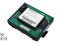
Fig. 24 DIN-rail mounting support DMBIMX15
NUCLEAR AND MEDICAL APPLICATIONS - These products are not designed or intended for use as critical components in life support systems, equipment used in hazardous environments, or nuclear control systems. TECHNICAL REVISIONS - The appearance of products, including safety agency certifications pictured on labels, may change depending on the date manufactured. Specifications are subject to change without notice. Copyright © 2017, Bel Power Solutions Inc. All rights reserved.
belfuse.com/power-solutions
Page 19 of 19