
1P503AS ANAREN
Document overview
- Manufacturer or author: Provided By digicamel.com
- PDF pages: 10
Technical content
Place Manufacturing. USA/Canada: Toll Free: Europe (315) 432 (800) 544 2414 +44 2392 232392 M odel 1 P50 3AS REV A Hybrid Couplers 3 dB, 90
Description
The 1P503AS Pico Xinger is a low profile, high performance 3dB hybrid coupler in an easy to use manufacturing friendly surface mount package. It is designed for DCS and PCS applications. The 1P503AS is designed for balanced amplifiers, variable phase shifters and attenuators, LNAs, signal distribution and is an ideal solution for the ever increasing demands of the wireless industry for smaller printed circuit boards and high performance. Parts have bee n subjected to rigorous qualification testing and they are manufactured using materials with coefficients of thermal expansion (CTE) compatible with common substrates such as FR4, G 10, RF 35, RO4003 and polyimide. Produced with 6 of 6 RoHS compliant tin immersion finish. ELECTRICAL SPECIFICATIONS** Features: 1.7 2.0 GHz. DCS and PCS Low Loss High Isolation 90° Quadrature Surface Mountable Tape And Reel Lead Free 100% Tested Frequency Isolation* Insertion Loss VSWR GHz dB Min dB Max Max:1 1.7 1.8 0.25 1.28 1.8 2.0 0.25 1.28 Amplitude Balance Phase Balance Power JC Operating Temp. dB Max Degrees Ave. CW Watts º C/Watt º C ± 0.45 27.5 55 to +85 ± 0.30 27.5 55 to +85 **Specification based on performance o f unit properly installed on microstrip printed circuit boards with 50 nominal impedance. Specifications subject to change without notice. Outline Drawing Part is Symmetric About All Axis Tolerances are Non Cumulative Dimensions are in Inches [Millimeters] P503 A S Mechanical Outline
USA/Canada: Toll Free: Europe: (315) 432 8909 (800) 544 2414 +44 2392 232392 Available on Tape and Reel For Pick and Place Manufacturing. Model P503 AS Rev. A Hybrid Coupler Pin Configuration The P503AS has an orientation marker to denote Pin 1. Once port one has been identified the other ports are known automatically. Please see the chart below for clarification: Configuration Pin 1 Pin 2 Pin 3 Pin 4 Splitter Input Isolated 3dB 3dB Splitter Isolated Input 3dB 3dB Splitter dB 3dB Input Isolated Splitter 3dB 3dB Isolated Input *Combiner A A Isolated Output *Combiner A A Output Isolated *Combiner Isolated Output A A *Combiner Output Isolated A A *Notes: “A” is the amplitude of the applied signal s. When two quadrature signals with equal amplitudes are applied to the coupler as described in the table, they will combine at the output port. If the amplitudes are not equal, some of the applied energy will be directed to the isolated port. The actual p hase, , or amplitude at a given frequency for all ports, can be seen in our de embedded s parameters, that can be downloaded at www.anaren.com
Place Manufacturing. USA/Canada: Toll Free: Europe (315) 432 (800) 544 2414 +44 2392 232392 M odel 1 P50 3AS REV A Typical Performance ( °C, 25°C & 125 °C): M Hz
USA/Canada: Toll Free: Europe: (315) 432 8909 (800) 544 2414 +44 2392 232392 Available on Tape and Reel For Pick and Place Manufacturing. Model P503 AS Rev. A Typical Performance ( °C, 25°C & 125 °C): 1700 2000 MHz
Place Manufacturing. USA/Canada: Toll Free: Europe (315) 432 (800) 544 2414 +44 2392 232392 M odel 1 P50 3AS REV A Definition of Measured Specifications Parameter Definition Mathematical Representation VSWR (Voltage Standing Wave Ratio) The impedance match of the coupler to a 50 system. A VSWR of 1:1 is optimal. VSWR = min max V V Vmax = voltage maxima of a standing wave Vmin = voltage minima of a standing wave Return Loss The impedance match of the coupler to a 50 system. Return Loss is an alternate means to express VSWR. Return Loss (dB)= 20log VSWR VSWR Insertion Loss The input power divided by the sum of the power at the two output ports. Insertion Loss(dB)= 10log direct cpl in P P P Isolation The input power divided by the power at the isolated port. Isolation(dB)= 10log iso in P P Phase Balance The difference in phase angle between the two outp ut ports. Phase at coupled port Phase at direct port Amplitude Balance The power at each output divided by the average power of the two outputs. 10log P P P direct cpl cpl and 10log P P P direct cpl direct
USA/Canada: Toll Free: Europe: (315) 432 8909 (800) 544 2414 +44 2392 232392 Available on Tape and Reel For Pick and Place Manufacturing. Model P503 AS Rev. A P503AS Power Derating Curv e 100 150 200 Mounting Interface Temperature ( o Power (Watts) Power Derating: The power handling and corresponding power derating plots are a function of the thermal resistance, mounting surface temperature (base plate temperature), maximum continuous operating temperature of the coupler, and the thermal insert ion loss. The thermal insertion loss is defined in the Power Handling section of the data sheet. As the mounting interface temperature approaches the maximum continuous operating temperature, the power handling decreases to zero.
Place Manufacturing. USA/Canada: Toll Free: Europe (315) 432 (800) 544 2414 +44 2392 232392 M odel 1 P50 3AS REV A Mounting I n order for Xinger surface mount couplers to work optimally, there must be 50 Ω transmission lines leading to and from all of the RF ports. Also, there must be a very good ground plane underneath the part to ensure proper electrical performance. If either of these two conditions is not satisfied, electrical perfor mance may not meet published specifications. Overall ground is improved if a dense population of plated through holes connect the top and bottom ground layers of the PCB. This minimizes ground inductance and improves ground continuity. All of the Xinger hybrid and directional couplers are constructed from ceramic filled PTFE composites which possess excellent electrical and mechanical stability having X and Y thermal coefficient of expansion (CTE) of 17 25 ppm/ o When a surface mount hybrid coupler is m ounted to a printed circuit board, the primary concerns are; ensuring the RF pads of the device are in contact with the circuit trace of the PCB and insuring the ground plane of neither the component nor the PCB is in contact with the RF signal. Mounting Footprint Coupler Mounting Process The process for assembling this component is a conventional surface mount process as shown in Figure 1. This process is conducive to both low and high volume usage. Figure 1: Surface Mounting Process Steps Storage of Components: Xinger products are available in either an immersion tin or tin lead finish. Commonly used storage procedures used to control oxidation should be followed for these surface mount com ponents. The storage temperatures should be held between 15 O C and O Substrate: Depending upon the particular component, the circuit material has an x and y coefficient of thermal expansion of between 17 and 25 ppm/°C. This coefficient minimizes solde r joint stresses due to similar expansion rates of most commonly used board substrates such as RF35, RO4003, FR4, polyimide and G 10 materials. Mounting to “hard” substrates (alumina etc.) is possible depending upon operational temperature requirements. Th e solder surfaces of the coupler are all copper plated with either an immersion tin or tin lead exterior finish. Solder Paste: All conventional solder paste formulations will work well with Anaren’s Xinger surface mount components. Solder paste can be app lied with stencils or syringe dispensers. An example of a stenciled solder paste deposit is shown in Figure 2. As shown in the figure solder paste is applied to the four RF pads and the entire ground plane underneath the body of the part.
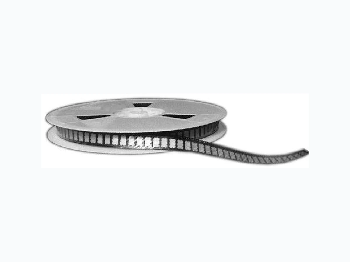
USA/Canada: Toll Free: Europe: (315) 432 8909 (800) 544 2414 +44 2392 232392 Available on Tape and Reel For Pick and Place Manufacturing. Model P503 AS Rev. A Packaging and Ordering Information Packaging follows EIA 481 2. Parts are oriented in tape as shown below. Minimum order quantities are 2000 per reel. Xinger Tape & Reel Diagram