
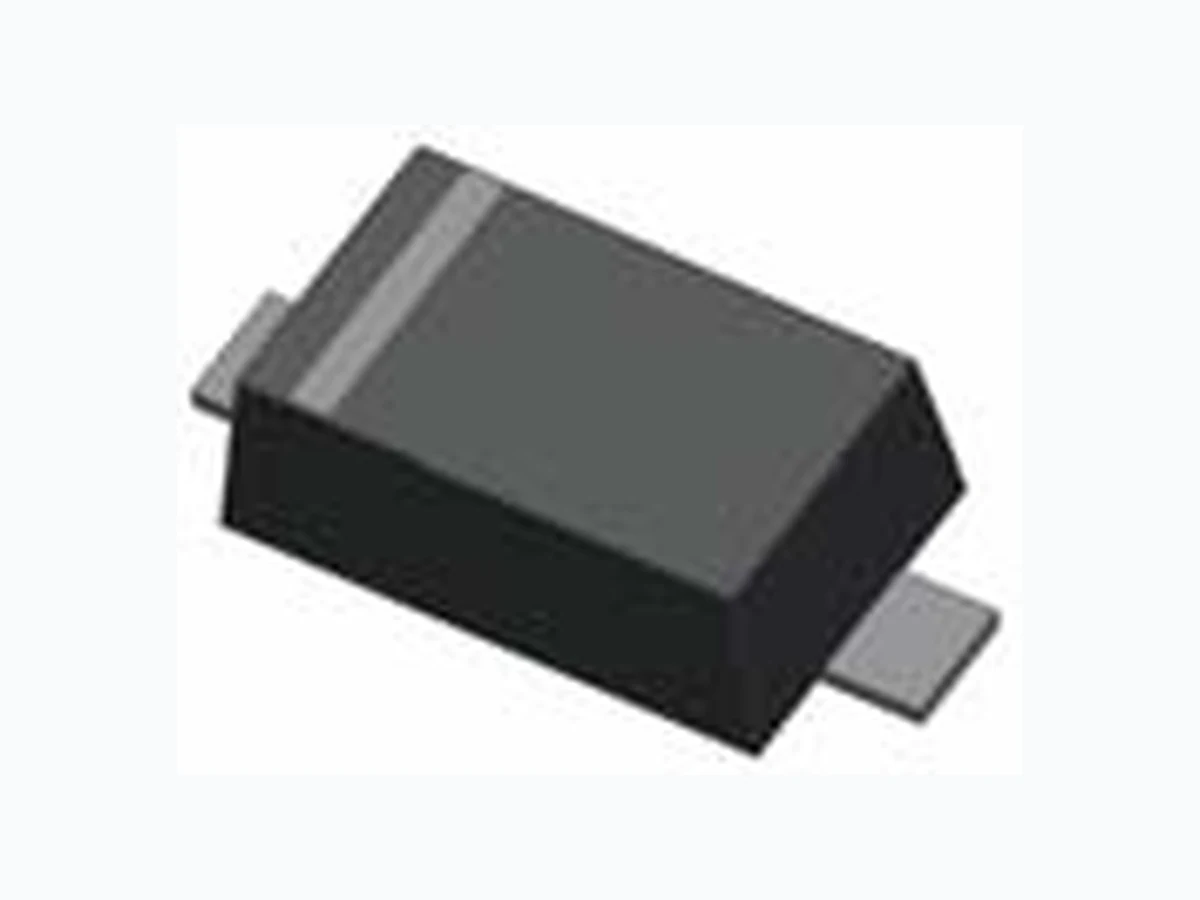
1N4148WS_10 TSC
Document overview
- Manufacturer or author: Provided By digicamel.com
- PDF pages: 3
Technical content
Features
Terminal: Matte tin plated, solderable per MIL-STD-202, Method 208 guaranteed Green compound (Halogen free) with suffix "G" on packing code and prefix "G" on date code High temperature soldering guaranteed: 260 °C/10s mA °C/W 100 mW V E Value 150 500 mA300 200 100 V Junction and Storage Temperature Range T J, TSTG -65 to + 150 Mean Forward Current Thermal Resistance (Junction to Ambient) IO RθJA VRRM IFRM VR Power Dissipation Reverse Voltage Non-Repetitive Peak Forward Current Repetitive Peak Reverse Voltage PD Type Number Polarity : Indicated by cathode band Weight : 4.85±0.5 mg Rating at 25°C ambient temperature unless otherwise specified.
Ordering Information
Unit (inch) Pin Configuration Marking Code : S1, S2, S3 Dimensions F Unit (mm) A B C D D A B C E F Version : E10
1N4148WS/1N4448WS/1N914BWS 200mW High Speed SMD Switching Diode Small Signal Diode
Electrical Characteristics
IR= IR= 1N4448WS, 1N914BWS I F= 1N4148WS I F= 1N4448WS, 1N914BWS I F= VR= VR= Junction Capacitance Tape & Reel specification Carrier depth Sprocket hole Reel outside diameter Reel inner diameter Feed hole width Sprocke hole position Punch hole position Sprocke hole pitch Embossment center Overall tape thickness Note 1: A0, B0, and K0 are determined by component size. The clearance between the components and the cavity must be Note 2: If B1 exceeds 4.2 mm(0.165'') for 8 mm embossed tape, the tape may not feed through all tape feeders. W 8.30 Max. Reel width W1 14.4 Max P0 4.00 ±0.10 P1 2.00 ±0.10 Tape width T 0.6 Max. 13.0 ± 0.5 K D E 1.75 ±0.10 50 Min. F 3.50 ±0.05 Item Symbol Dimension(mm) A 178 ± 1 2.40 Max. Min 1.5 ± 0.1 75 - UnitsMax ns4.0 Symbol 5.0 100 - -Reverse Recovery Time I F=10mA, IR=60mA, RL=100Ω, IRR=1mA Trr pF4.0 V 100.0mA 0.72 1.0 1.0- 10.0mA V R=0, f=1.0MHz V CJ 0.62 μA- VF IR V(BR) nA User Direction of Feed Reverse Breakdown Voltage Reverse Leakage Current Type Number 100uA 5uA Forward Voltage 20V 75V 5.0mA Top Cover Tape Carieer Tape Any Additional Label (If Required) TSC label D1D2A Version : E10
1N4148WS/1N4448WS/1N914BWS 200mW High Speed SMD Switching Diode Small Signal Diode Rating and Characteristic Curves FIG 1 Forward Voltage vs Forward Current 0.00 0.20 0.40 0.60 0.80 1.00 1.20 1.40 0.01 0.1 1 10 100 1000 Forward Current (mA) Forward Voltage (V) FIG 3 Admissible Power Dissipation Curve 100 150 200 250 0 25 50 75 100 125 150 175 Power Dissipation (mW) FIG 4 Typical Junction Capacitance 0.7 0.7 0.8 0.8 0.9 0.9 1.0 1.0 1.1 1.1 1.2 0123456789 1 0 Junction Capacitance (pF) Ambient Temperature (°C) Reverse Voltage (V) 25°C FIG 2 Reverse Current vs Reverse Voltage 0.01 0.1 100 0 20 40 60 80 100 120 Reverse Current (uA) Reverse Voltage (V) Ta=25°C VR=0V Tj=25°C f=1MHz 125° Version : E10