
DATASHEET SEARCH SITE
Document overview
- Manufacturer or author: Provided By digicamel.com
- PDF pages: 8
Technical content
T4-LDS-0303, Rev. 1 (6/14/13) ©2013 Microsemi Corporation Page 1 of 8 1N5820 – 1N5822 and 1N6864 Available on commercial versions
3 Amp Axial Schottky Barrier Rectifiers
Qualified per MIL-PRF-19500/620 Qualified Levels*: JAN, JANTX, JANTXV and JANS
DESCRIPTION
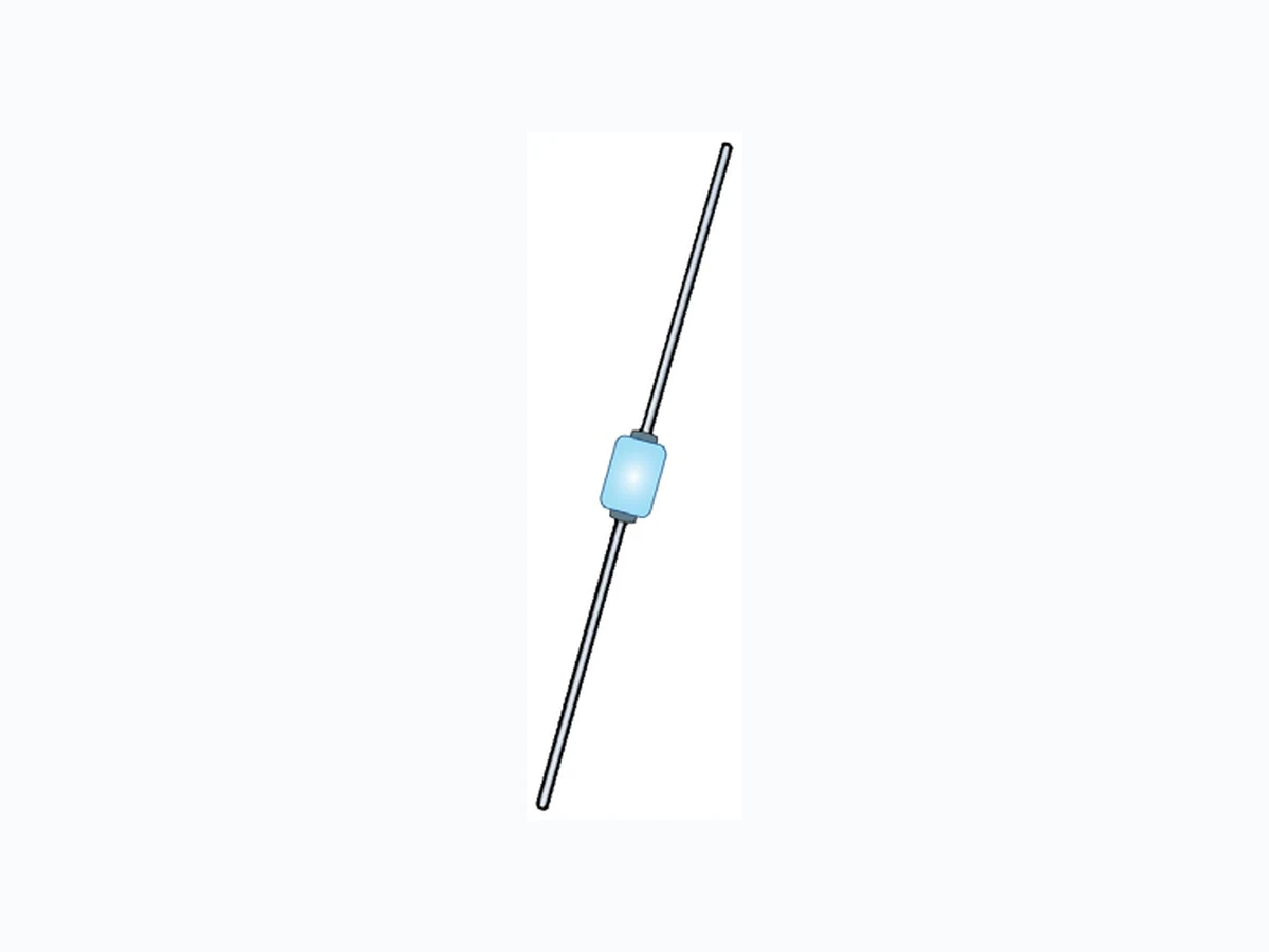
This series of 3 amp Schottky rectifiers in their axial-leaded “B” packaging offer flexible thru- hole mounting. The 1N5822 and 1N6864 are military qualified for high-reliability applications. “B” Package Also available in: “B” MELF Package (surface mount) 1N5820US – 1N5822US, 1N6864US Important: For the latest information, visit our website http://www.microsemi.com.
FEATURES
- JEDEC registered 1N5820 – 1N5822 and 1N6864 numbers.
- Hermetically sealed.
- Metallurgically bonded.
- Double plug construction.
- *JAN, JANTX, JANTXV and JANS qualifications are available per MIL-PRF-19500/620 for 1N6822 and 1N6864 only. (See Part Nomenclature for all available options.)
- RoHS compliant devices available (commercial grade only). APPLICATIONS / BENEFITS
- Flexible axial leads for thru-hole mounting (see package illustration).
- Non-sensitive to ESD per MIL-STD-750 method 1020. MAXIMUM RATINGS @ TA = +25 oC unless otherwise noted. MSC – Lawrence
6 Lake Street,
Lawrence, MA 01841 1-800-446-1158 Tel: (978) 620-2600 Fax: (978) 689-0803 MSC – Ireland Gort Road Business Park, Ennis, Co. Clare, Ireland Tel: +353 (0) 65 6840044 Fax: +353 (0) 65 6822298 Website: www.microsemi.com Parameters/Test Conditions Symbol Value Unit Junction Temperature TJ -65 to +125 oC Storage Temperature TSTG -65 to +150 oC Thermal Resistance Junction-to-Lead @ .375 inch (9.52 mm) lead length RӨJL 30 oC/W Surge Peak Forward Current @ TA = +25 oC (Test pulse = 8.3 ms, half-sine wave.) IFSM 80 A Average Rectified Output Current @ TL= +55 oC (1) IO 3 A NOTES: 1. See Figures 3 and 4 for derating curves and for effects of VR on TJ. The maximum TJ depends on the voltage applied.
T4-LDS-0303, Rev. 1 (6/14/13) ©2013 Microsemi Corporation Page 2 of 8 1N5820 – 1N5822 and 1N6864 MECHANICAL and PACKAGING
- CASE: Hermetically sealed voidless hard glass with tungsten slugs.
- TERMINALS: Tin/lead or RoHS compliant matte/tin on commercial grade only (no JAN levels) over nickel plate over copper.
- MARKING: Body coated in blue with part number.
- POLARITY: Cathode indicated by band.
- TAPE & REEL option: Standard per EIA-296. Consult factory for quantities.
- WEIGHT: Approximately 750 milligrams.
- See Package Dimensions on last page. PART NOMENCLATURE 1N5820 – 1N5821 1N5820 (e3) JEDEC type number See Electrical Characteristics table RoHS Compliance e3 = RoHS compliant Blank = non-RoHS compliant 1N5822 and 1N6864 only: JAN 1N5822 (e3) Reliability Level JAN = JAN Level JANTX = JANTX Level JANTXV = JANTXV Level JANS = JANS Level Blank = Commercial RoHS Compliance e3 = RoHS compliant (available on commercial grade only) Blank = non-RoHS compliant JEDEC type number (See Electrical Characteristics table) SYMBOLS & DEFINITIONS Symbol Definition CT Capacitance: The capacitance in pF at a frequency of 1 MHz and specified voltage. f frequency IR Maximum Reverse Current: The maximum reverse (leakage) current that will flow at the specified voltage and temperature. IO Average Rectified Output Current: The output current averaged over a full cycle with a 50 Hz or 60 Hz sine-wave input and a 180 degree conduction angle. VF Maximum Forward Voltage: The maximum forward voltage the device will exhibit at a specified current. VR Reverse Voltage: The dc voltage applied in the reverse direction below the breakdown region. VRWM Working Peak Reverse Voltage: The maximum peak voltage that can be applied over the operating temperature range.
T4-LDS-0303, Rev. 1 (6/14/13) ©2013 Microsemi Corporation Page 3 of 8 1N5820 – 1N5822 and 1N6864 ELECTRICAL CHARACTERISTICS @ 25 oC unless otherwise noted. TYPE NUMBER WORKING PEAK REVERSE VOLTAGE MAXIMUM FORWARD VOLTAGE VFM1 MAXIMUM FORWARD VOLTAGE VFM2 MAXIMUM FORWARD VOLTAGE VFM3 MAXIMUM REVERSE LEAKAGE CURRENT IRM @ VRM VRWM IFM = 1.0 A IFM = 3.0 A IFM = 9.4 A TJ = +25 ºC TJ = +100 ºC V (pk) Volts Volts Volts mA mA 1N6864 80 0.50 0.70 N/A 0.15 @ 80 V 18.0 @ 80 V
T4-LDS-0303, Rev. 1 (6/14/13) ©2013 Microsemi Corporation Page 7 of 8 1N5820 – 1N5822 and 1N6864 GRAPHS (continued) Pad Area per Pad (in2) FIGURE 7 Thermal resistance vs FR4 Pad Area Still Air with the PCB horizontal (At lead length = 0.187 inch) Thermal Resistance (C/W)
T4-LDS-0303, Rev. 1 (6/14/13) ©2013 Microsemi Corporation Page 8 of 8 1N5820 – 1N5822 and 1N6864 PACKAGE DIMENSIONS NOTES: 1. Dimensions are in inches. 2. Millimeters are given for information only. 3. Dimension BL shall include the entire body including slugs and sections of the lead over which the diameter is uncontrolled. This uncontrolled area is defined as the zone between the edge of the diode body and extending .050 inch (1.27 mm) onto the leads. 4. Dimension BD shall be measured at the largest diameter. 5. In accordance with ASME Y14.5M, diameters are equivalent to Φx symbology. DIMENSIONS Ltr INCH MILLIMETERS Notes Min Max Min Max BD 0.115 0.142 2.92 3.61 4 BL 0.130 0.300 3.30 7.62 3 LD 0.036 0.042 0.91 1.07 3 LL 0.900 1.30 22.86 33.02 Lead Tolerance = +.002 - .003 in. (Includes sections of the lead or fillet over which the lead diameter is uncontrolled.)