

 Download PDF
1N5817W KEXIN
Document overview
- Manufacturer or author: Provided By digicamel.com
- PDF pages: 3
Technical content
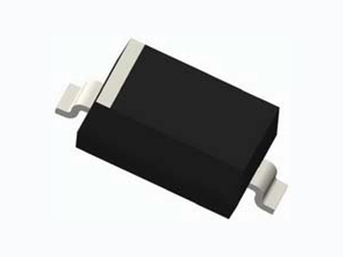
www.kexin.com.cn 1 DiodesSMD Type Schottky Diodes 1N5817W ~ 1N5819W Ƶ Features ƽ Low power loss, high efficiency ƽ High current capability ƽ Low forward voltage drop ƽ High Surge Capability Ƶ Absolute Maximum Ratings Ta = 25ć Parameter Symbol 1N5817W 1N5818W 1N5819W Unit Peak Repetitive Reverse Voltage V RRM 20 30 40 RMS Voltage V RMS 14 21 28 DC Blocking Voltage V DC 20 30 40 Forward Voltage @ I F=1A 0.45 0.55 0.6 Forward Voltage @ I F=3.1A 0.75 0.875 0.9 Average Forward Rectified Current @ TL=90ć IFAV Non-Repetitive Peak Forward Surge Current @8.3ms I FSM Typical Junction Capacitance C J pF Junction Temperature T J Storage Temperature range T stg Reverse Voltage Leakage Current I R ć A VF V mA 110 125 - 5 5t o1 2 5 Ta = 25ć Ta = 100ć Ƶ Marking NO. 1N5817W 1N5818W 1N5819W Marking 12A 13A 14A PIN DESCRIPTION Cathode Anode PIN DESCRIPTION Top View SOD-123 1 2
www.kexin.com.cn2 DiodesSMD Type Schottky Diodes 1N5817W ~ 1N5819W Ƶ Typical Characterisitics 10 100 Fig.5 Maximum Non-Repetitive Peak Forward Surage Current Peak A)Forward Surage Current ( Number of Cycles at 50Hz 8.3 ms Single Half Sine Wave (JEDEC Method) 0.1 0 0.4 0.5 0.7 Fig.3 Typical Forward Characteristic Instaneous Forward Current (A) Instaneous Forward Voltage (V) 0.1 1.0 T= 2 5J T =125 J 0.2 0.5 0.3 0.60.2 Fig.2 Typical Reverse Characteristics Instaneous Current ( ȝA)Reverse 20 40 60 800 T= 2 5J °C T= 7 5J °C T= 1 2 5J °C Percent of Rated Peak Reverse Voltage ˄˅ 100 10 0 101 10 2 10 3 10 4 Fig.4 Typical Junction Capacitance 0.1 Junction Capacitance (pF) Reverse Voltage (V) 100 200 500 1001 0.01 100 0.1 100 Fig.6- Typical Transient Thermal Impedance Transient Thermal Impedance ˄ /W˅°C t, Pulse Duration ˄sec˅ 0.1 1 10 Fig.1 Forward Current Derating Curve 0.2 0.4 0.6 0.8 1.0 1.2 0.0 25 50 75 100 125 150 Average Forward Current (A) Single phase half-wave 60 Hz resistive or inductive load Ambient Temperature ( °C)
www.kexin.com.cn 3 DiodesSMD Type Schottky Diodes 1N5817W ~ 1N5819W Ƶ Package Outline Dimensions Ƶ The Recommended Mounting Pad Size Note: 1.Controlling dimension in millimeters. 2.General tolerance:±0.05mm. 3.The pad layout is for reference purposes only. Plastic surface mounted package; 2 leads SOD-123 Min Max Mi nM a x A 1.050 1.250 0.041 0.049 A1 0.000 0.100 0.000 0.004 A2 1.050 1.150 0.041 0.045 b 0.450 0.650 0.018 0.026 c 0.080 0.150 0.003 0.006 D 1.500 1.700 0.059 0.067 E 2.600 2.800 0.102 0.110 E1 3.550 3.850 0.140 0.152 L L1 0.250 0.450 0.010 0.018 °8 °0 °8 ° 0.500 REF 0.020 REF Symbol Dimensions In Millimeters Dimensions In Inches