
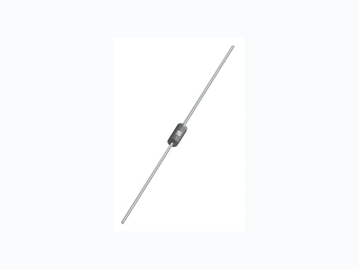
1N4740A_15 TSC
Document overview
- Manufacturer or author: Provided By digicamel.com
- PDF pages: 7
Technical content
- Glass passivated chip junction - Low profile package - Low inductance - Typical IR less than 5μA above 11V - Halogen-free according to IEC 61249-2-21 definition Molding compound, UL flammability classification rating 94V-0 Part No. with suffix "H" means AEC-Q101 qualified Packing code with suffix "G" means green compound (halogen-free) Terminal: Pure tin plated leads, solderable per JESD22-B102 Meet JESD 201 class 2 whisker test T J °C TSTG °C PART NO. PART NO. Document Number: DS_D1409040 Version: L15 AEC-Q101 qualified Green compound1N4740AHA0G 1N4740A H A0 G EXAMPLE PREFERRED PART NO. PART NO. SUFFIX PACKING CODE PACKING CODE SUFFIX
DESCRIPTION
DO-41 5000 / 13" Paper reel (Reverse) B0 DO-41 1000 / Bulk packing Note 1: "xx" defines voltage from 10V (1N4740A) to 200V (1M200Z) 1N47xxA 1MxxxZ (Note 1) H G DO-41 3000 / Ammo box (26mm taping) R0 DO-41 5000 / 13" Paper reel
ORDERING INFORMATION
PART NO. SUFFIX PACKING CODE PACKING CODE SUFFIX PACKAGE PACKING 1.0 6.67 UNIT
FEATURES
- Built-in strain relief - Compliant to RoHS Directive 2011/65/EU and in accordance to WEEE 2002/96/EC MECHANICAL DATA Case: DO-204AL (DO-41) Weight: 0.3g (approximately) PARAMETER MAXIMUM RATINGS AND ELECTRICAL CHARACTERSTICS (TA=25°C unless otherwise noted) VALUE Storage temperature range 1N4740A - 1M200Z Taiwan Semiconductor 1W, 10V - 200V Glass Passivated Junction Silicon Zener Diodes - 55 to +150 - 55 to +150 DO-204AL (DO-41) SYMBOL Note 1: Mounted on Cu-Pad size 5mm x 5mm on PCB Watts mW/°C Peak forward surge current, 8.3ms single half sine-wave superimposed on rated load IFSM Operating junction temperature range A Peak power dissipation at TA=50°C, Derate above 50°C (Note 1) PD
IZT ZZT@IZT IR mA ΩΩ mA μAV m A Notes: 1. Tolerance and Type Number Designation. The type numbers losted have a standard tolerance on the nominal zener voltage of ±5% 2. Specials Available Include: A. Nominal zener voltages between the voltages shown and tighter voltage tolerances B. Matched sets 3. Zener Voltage (Vz) Measurement. Guarantees the zener voltage when messured at 90 seconds while maintaining the lead temperature(T L) at 30°C±1°C, from the diode body 4. Zener Impedance (Zz) Derivation. The zener impedance is derives from the 60 cycle AC voltage, which results when an accurrent having and rms value equal to 10% of the DC zener current (IZT or IZK) is superimposed on IZT or IZK. 5. Surge Current (IR) Non-Repetitive. The rating listd in the electrical chatacteristics table is maximum peak, non-repetitive, reverse surge current of 1/2 square wave or equivalent sine wave pulse of 1/120 second duration superimposed on the test current, IZT per JEDEC registration; however, actual device capability is as described in Figure 11. Document Number: DS_D1409040 Version: L15 Min. ZZK@IZK MAXIMUM RATINGS AND ELECTRICAL CHARACTERISTICS (TA=25°C unless otherwise noted) Device (Note 1) Zener Voltage Vz@IzT V 1N4740A - 1M200Z Taiwan Semiconductor Zener Impedance Nom. (Note 2) (Note 3) Test Current Leakage Current I R@VR Max. Surge current Max.
(TA=25°C unless otherwise noted) Document Number: DS_D1409040 Version: L15 RATINGS AND CHARACTERISTICS CURVES 1N4740A - 1M200Z Taiwan Semiconductor 0.25 0.5 0.75 1.25 0 25 50 75 100 125 150 PD, MAXIMUM POWER DISSIPATION (WATTS) AMBIENT TEMPERATURE(oC) FIG. 1 POWER TEMPERATURE DERATING CURVE 100 1000 11 0 1 0 0 Zz, DYNAMIC IMPEDANCE (Ω) Iz, ZENER CURRENT(mA) FIG.4 EFFECT OF ZENER VOLTAGE ON ZENER IMPEDANCE Iz(rms)=0.1 Iz(dc) f=1KHzIz = 1mA 5 mA 20mA 100 1000 IF, FORWARD CURRENT (mA) VF, FORWARD VOLTAGE (V) FIG. 2 TYPICAL FORWARD CHARACTERISTICS MINIMUM MAXIMUM 0°C 25°C 70°C 150°C 100 1000 0 1 10 100 Zz, DYNAMIC IMPEDANCE (Ω) Iz, ZENER CURRENT (mA) FIG.3 EFFECT OF ZENER CURRENT ON ZENER IMPEDANCE Iz(rms)=0.1 Iz(dc) f=1KHz 47V 27V 0.8V 0.001 0.01 0.1 100 1000 10000 3456789 1 0 1 1 1 2 1 3 1 4 1 5 IR, LEAKAGE CURRENT(μA) Vz, NOMINAL ZENER VOLTAGE(V) FIG.5 TYPICAL LEAKAGE CURRENT TYPICAL LEAKAGE CURRENT AT 80% OF NOMINAL BREAKDOWN VOLTAGE 125°C 25°C
Document Number: DS_D1409040 Version: L15 1N4740A - 1M200Z Taiwan Semiconductor 100 1000 1 10 100 C, CAPACITANCE(pF) Vz, FORWARD VOLTAGE (V) FIG.6 TYPICAL CAPACITANCE versus Vz 50% OF BREAKDOWN 0V BIAS 1.0V BIAS 23456789 1 0 1 1 1 2 θVz, TEMPERATURE COEFFICIENT (mV/oC) Vz, ZENER VOLTAGE(V) FIG. 7 TEMPERATURE COEFFICIENTS a-RANGE FOR UNITS TO 12 VOLTS RANGE Vz@ IZT 100 10 100 θVz, TEMPERATURE COEFFICIENT (mV/oC) Vz, ZENER VOLTAGE(V) FIG.8 TEMPERATURE COEFFICIENTS RANGE Vz@ IZT b-RANGE FOR UNITS 12 TO 100 VOLTS θVz, TEMPERATURE COEFFICIENT (mV/℃) Vz, ZENER VOLTAGE(V) FIG. 9 EFFECT OF ZENER CURRENT NOTE:BELOW 3 VOLTAGE ABOVE a VOLTS CHANGES IN ZENER CURRENT NOT AFFECT TEMPERATURE COEFFICIENTS Vz@ IZT 0.01mA 1 mA 20mA 100 125 150 175 ΘJL, JUNCTION TO LEAD THERMAL RESISTANCE(oC/W) L, LEAD LENGTH TO HEAT SINK(INCHES) FIG. 10 TYPICAL THERMAL RESISTANCE versus LEAD LENGTH
Document Number: DS_D1409040 Version: L15 1N4740A - 1M200Z Taiwan Semiconductor 100 0 0 1 10 100 1000 PPK, PEAK SURGE POWER WATTS PW, PULSE WIDTH (ms) FIG.11 MAXIMUM SURGE POWER 20% DUTY CYCLE 11V-91V NON-REPETITIVE 10% DUTY CYCLE 5% DUTY CYCLE 0.8V-10V NON-REPETITIVE RECTANGULAR WAVEFORM PRIOR TO INITIAL PULSE
A 2.00 2.70 0.079 0.106 B 0.71 0.86 0.028 0.034 C 25.40 - 1.000 - D 4.20 5.20 0.165 0.205 E 25.40 - 1.000 - P/N = Specific Device Code G = Green Compound YWW = Date Code F = Factory Code Document Number: DS_D1409040 Version: L15 MARKING DIAGRAM DO-204AL (DO-41) 1N4740A - 1M200Z Taiwan Semiconductor PACKAGE OUTLINE DIMENSIONS DIM. Unit (mm) Unit (inch)
assumes no responsibility or liability for any errors or inaccuracies. Information contained herein is intended to provide a product description only. No license, express or implied, to any intellectual property rights is granted by this document. Except as provided in TSC's terms and conditions of sale for such products, TSC assumes no liability whatsoever, and disclaims any express or implied warranty, relating to sale and/or use of TSC products including liability or warranties relating to fitness for a particular purpose, merchantability, or infringement of any patent, copyright, or other intellectual property right. The products shown herein are not designed for use in medical, life-saving, or life-sustaining applications. Customers using or selling these products for use in such applications do so at their own risk and agree to fully indemnify TSC for any damages resulting from such improper use or sale. Document Number: DS_D1409040 Version: L15 1N4740A - 1M200Z Taiwan Semiconductor Notice Specifications of the products displayed herein are subject to change without notice. TSC or anyone on its behalf,