
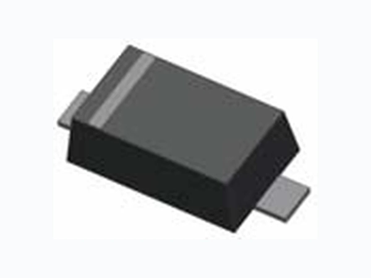
1N4X48WS TSC
Document overview
- Manufacturer or author: Provided By digicamel.com
- PDF pages: 3
Technical content
Features
Terminal: Matte tin plated, solderable per MIL-STD-202, Method 208 guaranteed Green compound (Halogen free) with suffix "G" on packing code and prefix "G" on date code High temperature soldering guaranteed: 260°C/10s mA °C/W 100 mW V E Value 150 500 mA300 200 100 V Junction and Storage Temperature Range T J , T STG -65 to + 150 Mean Forward Current Thermal Resistance (Junction to Ambient) I O RθJA V RRM I FRM V R Power Dissipation Reverse Voltage Non-Repetitive Peak Forward Current Repetitive Peak Reverse Voltage P D Type Number Polarity : Indicated by cathode band Weight : 4.85±0.5 mg Rating at 25°C ambient temperature unless otherwise specified.
Ordering Information
Unit (inch) Pin Configuration Marking Code : S1, S2, S3 Dimensions F Unit (mm) A B C D D A B C E F Version : F12
1N4148WS/1N4448WS/1N914BWS 200mW High Speed SMD Switching Diode Small Signal Diode
Electrical Characteristics
I R I R 1N4448WS, 1N914BWS I F 1N4148WS I F 1N4448WS, 1N914BWS I F V R V R Junction Capacitance Tape & Reel specification Carrier depth Sprocket hole Reel outside diameter Reel inner diameter Feed hole width Sprocke hole position Punch hole position Sprocke hole pitch Embossment center Overall tape thickness Note 1: A0, B0, and K0 are determined by component size. The clearance between the components and the cavity must be Note 2: If B1 exceeds 4.2 mm(0.165'') for 8 mm embossed tape, the tape may not feed through all tape feeders. W 8.30 Max. Reel width W1 14.4 Max P0 4.00 ±0.10 P1 2.00 ±0.10 0.6 Max. 13.0 ± 0.5 E 1.75 ±0.10 D Tape width T 50 Min. F 3.50 ±0.05 Item Symbol Dimension(mm) A 178 ± 1 2.40 Max.K Min 1.5 ± 0.1 75 - UnitsMax ns4.0 Symbol 5.0 100 - -Reverse Recovery Time I F =10mA, I R =60mA, R L =100Ω, I RR =1mA Trr pF4.0 V 100.0mA 0.72 1.0 1.0- 10.0mA V R =0, f=1.0MHz V C J 0.62 μA- V F I R V (BR) nA User Direction of Feed Reverse Breakdown Voltage Reverse Leakage Current Type Number 100uA 5uA Forward Voltage 20V 75V 5.0mA Top Cover Tape Carieer Tape An y Additional Label If Required TSC label D1D2A Version : F12
1N4148WS/1N4448WS/1N914BWS 200mW High Speed SMD Switching Diode Small Signal Diode Rating and Characteristic Curves FIG 1 Forward Voltage vs Forward Current 0.00 0.20 0.40 0.60 0.80 1.00 1.20 1.40 0.01 0.1 1 10 100 1000 Forward Current (mA) Forward Voltage (V) FIG 3 Admissible Power Dissipation Curve 100 150 200 250 0 25 50 75 100 125 150 175 Power Dissipation (mW) FIG 4 Typical Junction Capacitance 0.7 0.7 0.8 0.8 0.9 0.9 1.0 1.0 1.1 1.1 1.2 0123456789 1 0 Junction Capacitance (pF) Ambient Temperature (°C) Reverse Voltage (V) 25°C FIG 2 Reverse Current vs Reverse Voltage 0.01 0.1 100 0 20 40 60 80 100 120 Reverse Current (uA) Reverse Voltage (V) Ta=25°C V R =0V Tj=25°C f=1MHz 125° Version : F12