
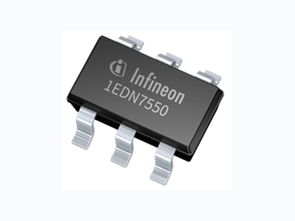
1EDN7550 INFINEON
Document overview
- Manufacturer or author: Provided By digicamel.com
- PDF pages: 27
Technical content
Features
- Very large common-mode input voltage range (CMR) up to ± 150 V ( Table 1)
- Supply voltage ( VDD) up to 20 V
- 2 UVLO options: 4 V and 8 V
- Separate low impedance source and sink outputs - 4 A / 0.85 Ω source - 8 A / 0.35 Ω sink
- 45 ns propagation delay with -7 / +10 ns accuracy
- SOT23 or TSNP 6-pin package
- Fully qualified for industrial applications according to JEDEC
Description
EiceDRIVER™ 1EDNx550 is a new family of single-channel non-isolated gate-driver ICs. Due to the unique fully differential input circuitry with excellent common-mode rejection, the logic driver state is exclusively controlled by the voltage difference between the two inputs, completely independent of the driver’s reference (ground) potential. This eliminates the risk for false triggering and thus is a significant benefit in all applications exhibiting voltage differences between driver and controller ground, a problem typical for systems with
- 4-pin packages (Kelvin Source connection)
- high parasitic PCB inductances (long distances, single-layer PCB)
- bipolar gate drive In addition, within the common-mode voltage range CMR for PWM signal at 3.3 V as in (Table 1), 1EDNx550 allows to address even high-side and half-bridge applications. For PWM signals other than 3.3. V please see the Application note Applications of 1EDNx550 single-channel lowside EiceDRIVER™ with truly differential inputs. Table 1 Product portfolio Part number CMR static CMR dynamic UVLO Package 1EDN7550B + 72 V / - 84 V ± 150 V 4 V PG-SOT23-6 1EDN8550B + 72 V / - 84 V ± 150 V 8 V PG-SOT23-6 1EDN7550U + 72 V / - 84 V ± 150 V 4 V PG-TSNP-6 IN+ OUT_SNK V DD IN- R gon R goff 1EDNx550 R in1 SGND D V Rin GND C VDD Z VDD R in2 VDD OUT_SR C Figure 1 Typical application Datasheet Please read the Important Notice and Warnings at the end of this document Rev. 2.2 www.infineon.com 2019-12-09
EiceDRIVER™ 1EDN7550 and 1EDN8550 Single-channel EiceDRIVER™ gate-drive IC with true differ ential inputs Table of contents Datasheet 2 Rev. 2.2 2019-12-09
1 Pin configuration and description
The pin configuration for both SOT23 and TSNP package is illustrated in Figure 2; a description is given in Table 2 . For functional details, please read Chapter 3. IN- GND IN+ OUT_SNK OUT_SRC VDD SOT23-6 1 6 TSNP-6 IN- GND IN+ OUT_SNK OUT_SRC VDD 1 6 3 4 Figure 2 Pin configuration SOT23 and TSNP 6-pin packages (top view) Table 2 Pin description Pin number Pin name Description
1 IN- Negative input
connected to controller ground via resistor (typically 33 kΩ)
2 GND Ground
negative gate drive voltage ("off" state)
3 IN+ Positive input
connected to PWM output of controller via resistor (typically 33 kΩ)
4 VDD Positive supply voltage
positive gate drive voltage ("on" state)
5 OUT_SRC Driver output source
low-impedance switch to VDD (4 A / 0.85 Ω)
6 OUT_SNK Driver output sink
low-impedance switch to GND (8 A / 0.35 Ω) EiceDRIVER™ 1EDN7550 and 1EDN8550 Single-channel EiceDRIVER™ gate-drive IC with true differ ential inputs Pin configuration and description Datasheet 3 Rev. 2.2 2019-12-09
2 Block diagram
A simplified functional block diagram of 1EDNx550 is given in Figure 3. IN+ IN- GND VDD OUT_SNK OUT_SRC Differential Schmitt Trigger Diff. Amp. + LPF UVLO Logic Figure 3 Block diagram EiceDRIVER™ 1EDN7550 and 1EDN8550 Single-channel EiceDRIVER™ gate-drive IC with true differ ential inputs Block diagram Datasheet 4 Rev. 2.2 2019-12-09
3 Functional description
Although EiceDRIVER™ 1EDNx550 is a family of non-isolated gate drivers, it extends the range of possible applications into fields usually reserved for isolated drivers, thereby generating significant system cost benefits. The key to make this possible is moving from the standard ground related to a true differential input with very high common-mode rejection. The required symmetry of the input circuitry is achieved by on-chip trimming; it finally allows to deal with peak common-mode voltages of up to ± 150 V between driver reference (GND) and system ground (SGND). 1EDNx550 is not only ideally suited for any application with unwanted shifts between driver and system ground, but may also be utilized as a high-side driver within the allowed common-mode range. Besides, switches requiring a bipolar driving voltage can be operated very easily as well.
3.1 Differ ential input
Figure 4 depicts the signal path from the controller’s PWM output to the logic gate driver signal as implemented on 1EDNx550. IN+ IN- Differential Schmitt Trigger A v = 4.5
12 MHz
Figure 4 1EDNx550 input signal path The controller output signal, switching between controller supply VS and zero, is applied at the one leg of a differential voltage divider, while the other is connected to the controller ground SGND. The divider ratio has to be adapted to VS to allow a fixed Schmitt-Trigger threshold voltage. For VS = 3.3 V, Rin1 and Rin2 are chosen to be 33 kΩ, resulting in a static divider ratio of k = 12 at the driver inputs and 36 at the internal voltage amplifier. With VS other than 3.3 V, Rin has to fulfil the relation: Rin1 = Rin2 = 10.9 VS−3 kΩ Amplified by a factor of 4.5, the signal is filtered by a 2nd order low-pass filter. Taking into account the RC filter in front of the amplifier, the overall input path exhibits the frequency behavior of a 3rd order low-pass filter with a corner frequency around 12 MHz. The suppression of high frequencies is important for two reasons. Firstly, common-mode ringing, being in the 100 MHz and above range for fast-switching power systems, can effectively be damped. In addition, the high-frequency symmetry of the voltage divider is influenced by parasitic capacitances, particularly Cp1 and Cp2, the parallel capacitances of Rin1 and Rin2. They are typically in the 50 to 100 fF range, rather independent of resistor size. Without filtering, any asymmetry would translate high- frequency common-mode into differential signals. The filtered signal is then applied to a differential Schmitt-Trigger with accurate trimmed threshold levels and converted to the logic switch control signal. The subsequent pulse extender function guarantees that no pulses shorter than 25 ns are transmitted to the output, thereby further improving noise immunity. Due to the filtering requirements the input-to-output propagation delay is slightly increased to around 45 ns. By means of on-chip trimming, however, the usually more relevant propagation delay variation can still be kept low at +10 / -7 ns. EiceDRIVER™ 1EDN7550 and 1EDN8550 Single-channel EiceDRIVER™ gate-drive IC with true differ ential inputs Functional description Datasheet 5 Rev. 2.2 2019-12-09
3.1.1 Common mode input range
There are two effects limiting the common-mode input range, i.e. the maximum allowed voltage difference between controller outputs PWM/SGND and driver reference GND: the circuit and technology-related input voltage restrictions and the finite common-mode rejection in the input signal path due to asymmetries. The static voltage range at the input pins is limited to + 6 / - 7 V to guarantee accurate linear operation of the input circuitry. Taking into account the proposed DC voltage divider ratio, this translates to a static common- mode (CMR) range of + 72 / - 84 V. CMR is increased even further for high-frequency common-mode voltages ("ringing"). Then the maximum input voltage ratings ( ± 10 V) together with the frequency-dependence of the voltage-divider ratio result in an extended dynamic CMR as high as ± 150 V. The second limitation results from the fact that any imbalance in the signal path converts a common-mode to a differential signal. To utilize the full CMR as calculated above, the high accuracy of the trimmed on-chip network must not be affected by the external voltage divider resistors. This condition is easily fulfilled when choosing Rin1 and Rin2 with 0.1% tolerance; resistors with only 1% accuracy, however, would reduce the common-mode range significantly to ± 40 V.
3.2 Driver outputs
The rail-to-rail driver output stage realized with complementary MOS transistors is able to provide a typical 4 A sourcing and 8 A sinking current. The low on-resistance coming together with high driving current is particularly beneficial for fast switching of very large MOSFETs. With a Ron of 0.85 Ω for the sourcing pMOS and 0.35 Ω for the sinking nMOS transistor the driver can in most applications be considered to behave like an ideal switch. The p-channel sourcing transistor allows real rail-to-rail behavior without suffering from the source-follower’s voltage drop typical for n-channel output stages. In case of floating inputs or insufficient supply voltage the driver output is actively clamped to the “low” level (GND).
3.3 Supply voltage and Undervoltage Lockout (UVLO)
The Undervoltage Lockout function ensures that the output can be switched only, if the supply voltage VDD exceeds the UVLO threshold voltage. Thus it can be guaranteed that the switch transistor is not operated with a driving voltage too low to achieve a complete and fast transition to the "on" state; this avoids excessive power dissipation (see Table 3). Table 3 Logic table ΔVRin UVLO OUT_SRC OUT_SNK x active1) high impedance L L2) inactive 3) high impedance L H4) inactive 3) H high impedance EiceDRIVER™ 1EDNx550 is available in two different packages; the SOT23 version offers 2 UVLO threshold levels to support switches with a broad range of threshold voltages
- 1EDN7550 with a typical UVLO threshold of 4.2 V (0.3 V hysteresis)
- 1EDN8550 with a typical UVLO threshold of 8 V (1 V hysteresis) In addition, the high maximum VDD of 20 V makes the driver family well suited for a broad variety of power switch types.
1 VDD < UVLOoff
2 ΔVRin < ΔVRinL
3 VDD > UVLOon
4 ΔVRin > ΔVRinH EiceDRIVER™ 1EDN7550 and 1EDN8550 Single-channel EiceDRIVER™ gate-drive IC with true differ ential inputs Functional description Datasheet 6 Rev. 2.2 2019-12-09
4 Electrical characteristics and parameters
The absolute maximum ratings are listed in Table 4 . Stresses beyond these values may cause permanent damage to the device. Exposure to absolute maximum rating conditions for extended periods may affect device reliability.
4.1 Absolute maximum ratings
Table 4 Absolute Maximum Ratings Parameter Symbol Values Unit Note or Test Condition Min. Typ. Max. Supply voltage VDD -0.3 – 22 V Voltage between VDD to GND Voltage at pins IN+ and IN- VIN -10 – 10 V – Voltage at pin OUT_SRC VOUT_SRC -24 – 0.3 V OUT = low; referred to VDD pin, DC -24 – 2 V OUT = low; referred to VDD pin < 200 ns Voltage at pin OUT_SNK VOUT_SNK -0.3 – 24 V OUT = high; referred to GND pin, DC -2 – 24 V OUT = high, referred to GND pin < 200 ns Peak reverse current at OUT_SRC ISRC_rev -5 – – A < 500 ns Peak reverse current at OUT_SRC ISRC_rev – – 5 A < 500 ns Junction temperature Tj -40 – 150 °C – Storage temperature TS -55 – 150 °C – ESD capability VESD_HBM – – 2 kV Human Body Model (HBM)5) ESD capability VESD_CDM – – 1 kV Charged Device Model (CDM)6) 5 According to ANSI/ESDA/JEDEC JS-001 (discharging 100 pF capacitor through 1.5 kΩ resistor)
6 According to ANSI/ESDA/JEDEC JS-002
EiceDRIVER™ 1EDN7550 and 1EDN8550 Single-channel EiceDRIVER™ gate-drive IC with true differ ential inputs Electrical characteristics and parameters Datasheet 7 Rev. 2.2 2019-12-09
4.2 Thermal characteristics
Table 5 Thermal characteristics SOT23 package Parameter Symbol Values Unit Note or Test Condition Min. Typ. Max. Thermal resistance junction- ambient7) RthJA25 – 165.1 – K/W – Thermal resistance junction- case (top)8) RthJC25 – 79.9 – K/W – Thermal resistance junction- board9) RthJB25 – 65.2 – K/W – Characterization parameter junction-case (top)10) ΨthJC25 – 14 – K/W – Characterization parameter junction-board11) ΨthJB25 – 51 – K/W – Table 6 Thermal characteristics TSNP package Parameter Symbol Values Unit Note or Test Condition Min. Typ. Max. Thermal resistance junction- ambient 7) RthJA25 – 141 – K/W – Thermal resistance junction- case (top) 8) RthJC25 – 81 – K/W – Thermal resistance junction- board 9) RthJB25 – 36 – K/W – Characterization parameter junction-case (top) 10) ΨthJC25 – 80 – K/W – Characterization parameter junction-board 11) ΨthJB25 – 36 – K/W – 7 Obtained in a simulation on a JEDEC-standard, high-K board, as specified in JESD51-7, in an environment described in JESD51-2a 8 Obtained by simulating a cold plate test on the package top. No specific JEDEC standard test exists, but a close description can be found in the ANSI SEMI standard G30-88 9 Obtained by simulation in an environment with a ring cold plate fixture to control the PCB temperature, as described in JESD51-8 10 Estimates the junction temperature of a device in a real system and is extracted from the simulation data for obtaining Rth, using a procedure described in JESD51-2a (sections 6 and 7) 11 Estimates the junction temperature of a device in a real system and is extracted from the simulation data for obtaining Rth, using a procedure described in JESD51-2a (sections 6 and 7) EiceDRIVER™ 1EDN7550 and 1EDN8550 Single-channel EiceDRIVER™ gate-drive IC with true differ ential inputs Electrical characteristics and parameters Datasheet 8 Rev. 2.2 2019-12-09
4.3 Operating range
Parameter Symbol Values Unit Note or Test Condition Min. Typ. Max. Supply voltage VDD 4.5 – 20 V Min defined by UVLO Voltage at pins IN+ and IN- VIN -7 – 6 V – Junction temperature Tj -40 – 150 °C 12)
4.4 Electrical characteristics
Unless otherwise noted, min./max. values of characteristics are the lower and upper limits, respectively. They are valid within the full operating range. The supply voltage is VDD= 12 V. Typical values are given at Tj=25°C. Table 8 Power Supply Parameter Symbol Values Unit Note or Test Condition Min. Typ. Max. VDD quiescent current IVDDh – 1.1 – mA OUT = high VDD quiescent current IVDDl – 0.9 – mA OUT = low Table 9 Undervoltage Lockout 1EDN7550x (Logic level MOSFET) Parameter Symbol Values Unit Note or Test Condition Min. Typ. Max. Undervoltage Lockout (UVLO) turn on threshold UVLOon 3.9 4.2 4.5 V – Undervoltage Lockout (UVLO) turn off threshold UVLOoff – 3.9 – V – UVLO threshold hysteresis UVLOhys 0.25 0.3 0.35 V – Table 10 Undervoltage Lockout 1EDN8550B (Standard MOSFET) Parameter Symbol Values Unit Note or Test Condition Min. Typ. Max. Undervoltage Lockout (UVLO) turn on threshold UVLOon 7.4 8.0 8.6 V – Undervoltage Lockout (UVLO) turn off threshold UVLOoff – 7.0 – V – UVLO threshold hysteresis UVLOhys 0.8 1.0 1.2 V –
12 Continuous operation above 125°C may reduce life time
EiceDRIVER™ 1EDN7550 and 1EDN8550 Single-channel EiceDRIVER™ gate-drive IC with true differ ential inputs Electrical characteristics and parameters Datasheet 9 Rev. 2.2 2019-12-09
Table 11 Inputs IN+, IN- Parameter Symbol Values Unit Note or Test Condition Min. Typ. Max. Differential input voltage threshold for transition LH (at input resistor) ∆VRinH – 1.7 – V Independent of VDD Rin1/Rin2 = 33 kΩ 13) Differential input voltage threshold for transition HL (at input resistor) ∆VRinL – 1.5 – V Independent of VDD Rin1/Rin2 = 33 kΩ 13) Total input resistance on each leg Rin1 / Rin2 – 36 – kΩ Rin1/Rin2 = 33 kΩ 13) Table 12 Static Output Characteristics Parameter Symbol Values Unit Note or Test Condition Min. Typ. Max. High-level (sourcing) output resistance Ron_SRC – 0.85 – Ω ISRC = 50 mA Sourcing output current ISRC_pk – 4.0 14) A – Low-level (sinking) output resistance Ron_SNK – 0.35 – Ω ISNK = 50 mA Sinking output current ISNK_pk – -8.0 15) A – Table 13 Dynamic characteristics Parameter Symbol Values Unit Note or Test Condition Min. Typ. Max. Input-to-output propagation delay turn-on tPDon 38 45 55 ns CL = 200 pF Input-to-output propagation delay turn-off tPDoff 38 45 55 ns CL = 200 pF Rise time trise — 6.5 1516) ns CL = 1.8 nF Fall time tfall — 4.5 1516) ns CL = 1.8 nF Rise time trise — 1 516) ns CL = 200 pF Fall Time tfall — 1 516) ns CL = 200 pF Minimum input pulse width that changes output state tPW — 2516) — ns CL = 1.8 nF For an illustration of the dynamic characteristics see Figure 6 and Figure 7 Figure 5 gives the circuit used for parameter testing
13 See Figure 1
14 Actively limited to approx. 5.2 Apk; not subject to production test - verified by design / characterization 15 Actively limited to approx. -10.4 Apk; not subject to production test - verified by design / characterization
16 Parameter verified by design, not 100% tested in production
EiceDRIVER™ 1EDN7550 and 1EDN8550 Single-channel EiceDRIVER™ gate-drive IC with true differ ential inputs Electrical characteristics and parameters Datasheet 10 Rev. 2.2 2019-12-09
4.5 Timing diagram
Figure 6 depicts rise, fall and delay times as given in the Chapter 4. IN+ - IN- OUTx t PDon 50% t PDoff 10% 90% t rise t fall 1.7 1.5 Figure 6 Propagation delay, rise and fall time Figure 7 illustrates the Undervoltage Lockout function. OUTx V DD UVLO on UVLO off Figure 7 UVLO behavior (output state high) EiceDRIVER™ 1EDN7550 and 1EDN8550 Single-channel EiceDRIVER™ gate-drive IC with true differ ential inputs Electrical characteristics and parameters Datasheet 11 Rev. 2.2 2019-12-09
5 Typical characteristics
- Undervoltage Lockout threshold (1EDN7550) vs temperature 2. Undervoltage Lockout threshold (1EDN8550) vs temperature 3.7 3.9 4.1 4.3 4.5 -50 0 50 100 150 VDD [V] Tj [ °C] UVLO on UVLO off 6.4 6.8 7.2 7.6 8.0 8.4 8.8 -50 0 50 100 150 VDD [V] Tj [°C] UVLO on UVLO off 3. Differ ential input voltage threshold vs temperature 4. Typical quiescent current vs temperature 1.1 1.3 1.5 1.7 1.9 2.1 2.3 2.5 -50 0 50 100 150 Tj [°C] ON threshold OFF threshold VDD=12V Vin=3.3V ∆ VRin [V] 0.6 0.8 1.0 1.2 1.4 -50 0 50 100 150 Tj [ °C] OUT High OUT Low IVDD [mA] EiceDRIVER™ 1EDN7550 and 1EDN8550 Single-channel EiceDRIVER™ gate-drive IC with true differ ential inputs Typical characteristics Datasheet 12 Rev. 2.2 2019-12-09
- Typical quiescent current vs supply voltage 6. Total operating current consumption with capacitive load vs frequency 0.6 0.7 0.8 0.9 1.0 1.1 1.2 1.3 1.4 1.5 1.6 0 5 10 15 20 25 VDD [V] OUT High OUT Low IVDD [mA] 0 200 400 600 800 1000 Frequency [kHz] VDD 4.5V VDD 12V VDD 20V Duty Cycle 50% CL = 1.8nF IVDD [mA] 7. Typical propagation delay vs temperature 8. Typical rise and fall time vs temperature -50 0 50 100 150 Tj [ °C] turn-on turn-off VDD=12V Vin=3.3V tPD [ns] -50 0 50 100 150 Tj [°C] turn-on turn-off VDD=12V CL=1.8nF trise/fall [ns] EiceDRIVER™ 1EDN7550 and 1EDN8550 Single-channel EiceDRIVER™ gate-drive IC with true differ ential inputs Typical characteristics Datasheet 13 Rev. 2.2 2019-12-09
6 Typical applications
6.1 Switches with Kelvin source connection (4-pin packages)
This is one of the key target applications of 1EDNx550. The 4-pin configuration depicted in Figure 8 is a very effective measure to improve the switching performance of transistors in packages with high source inductance LS as is typical for the widely used TO-packages. Although the Kelvin Source connection SS solves the problem of the largely increased switching losses due to LS, it is evident, that the gate driver reference potential is moving by the inductive voltage drop vLS with respect to the system ground SGND. In fast-switching applications at high current, vLS can reach 100 V and above. This is why 4-pin systems so far either used isolated drivers or external filters with relatively low corner frequency that add significant signal delay. Now, however, 1EDNx550 provides an optimum solution for this case. Figure 8 also indicates that the usually SGND-related VDD cannot be used directly as the driver supply. But due to the high frequency of vLS (> 100 MHz), a filter composed of impedance ZVDD together with the blocking cap CVDD is well suited to generate a sufficiently stable driver supply. ZVDD can be either a resistor (e.g. 22 Ω with a typical CVDD of 1 µF) or, even better, a proper ferrite bead. IN+ OUT_SNK V DD IN- R gon R goff 1EDNx550 R in1 SGND ΔV Rin GND C VDD Z VDD R in2 VDDPWM_Out SGND Controller v LS L S MOSFET D G S SS OUT_SRC Figure 8 1EDN driving 4-pin MOSFET
6.2 Applications with significant parasitic PCB-inductances
In fast switching power systems the unavoidable parasitic inductance associated with any electrical connection may cause significant inductive voltage drops, particularly if the PCB-layout cannot be optimized, the most common reasons being limitations in the number of PCB-layers, geometric restrictions or also the lack of specific experience. In such situations the high robustness of 1EDNx550 with respect to “switching noise” (high- frequency voltage between reference potential of driver and controller) is extremely valuable and allows good performance even in systems with formerly critical layout. Figure 9 indicates a respective example, indicating the most relevant parasitic PCB-inductances. EiceDRIVER™ 1EDN7550 and 1EDN8550 Single-channel EiceDRIVER™ gate-drive IC with true differ ential inputs Typical applications Datasheet 14 Rev. 2.2 2019-12-09
OUT_SNK V DD IN- R gon R goff 1EDNx550 R in1 SGND D V Rin GND C VDD Z VDD R in2 VDD OUT_SR C PWM_Out SGND Controller MOSFET D G S Figure 9 Application with significant PCB inductance
6.3 Switches with bipolar gate drive
Another application 1EDNx550 is tailored for, is driving power switches that require a negative gate-to-source voltage to safely hold them in the “off” state. Although MOSFETs are usually operated at zero “off” voltage, in certain situations a negative gate drive voltage can be very helpful. Particularly the fast switching “off” of high current when using switches with large common source inductance (e.g. in 3-pin TO-packages) may become critical in terms of losses and stability with a zero “off” level. In such cases a negative gate drive voltage is able to significantly improve switching performance. As depicted in Figure 10, this kind of application is completely uncritical and handled easily with 1EDNx550, while standard drivers cannot be applied directly without adaptations. IN+ OUT_SNKIN- R gon R goff 1EDNx550 R in1SGND ΔV Rin GND R in2 VDDPWM_Out SGND Controller OUT_SRC MOSFET D G S Figure 10 Bipolar gate drive for 3-pin MOSFET EiceDRIVER™ 1EDN7550 and 1EDN8550 Single-channel EiceDRIVER™ gate-drive IC with true differ ential inputs Typical applications Datasheet 15 Rev. 2.2 2019-12-09
6.4 High-side switches
Due to the large static input common-mode range, even driving high-side switches is an interesting application field for 1EDNx550. Although not providing galvanic isolation, 1EDNx550 can functionally be used as a high-side driver, as long as the power-loop voltage VP does not cause a violation of the allowed common-mode range. In high-side operation as depicted in Figure 11, the driver ground GND switches between zero (“off” ) and VP (“on" state) with respect to SGND; the resulting common-mode voltage at the driver input pins is 0 and -VP/12, respectively. The input voltage restriction to -7 V (Table 7) thus limits VP to 84 V. In many applications the driver supply voltage can be generated by means of the well-known bootstrapping method also indicated in Figure 11. IN+ OUT_SNK V DD IN- R gon R goff 1EDNx550 R in1SGND ΔV Rin GND C boot R boot R in2 VDDPWM_Out SGND Controller OUT_SRC D G S D G S V P < 84V V sw D boot Figure 11 1EDNx550 as a high-side driver EiceDRIVER™ 1EDN7550 and 1EDN8550 Single-channel EiceDRIVER™ gate-drive IC with true differ ential inputs Typical applications Datasheet 16 Rev. 2.2 2019-12-09
7 Layout guidelines
It is well-known that the layout of a fast-switching power system is a critical task with strong influence on the overall performance. This is why there exists a huge number of rules, recommendations, guidelines, tips and tricks that should help to finally end up with a proper system layout. With 1EDNx550 one of the central layout problems, namely the design of the grounding network, has become much less critical due to the highly reduced sensitivity of the differential concept with respect to ground voltage differences. So layout rules can be restricted to the following rather simple and evident ones:
- place input resistors Rin close to the driver and make layout of input signal path as symmetric and as compact as possible
- use a low-ESR decoupling capacitance for the VDD supply and place it as close as possible to the driver
- minimize power loop inductance as the most critical limitation of switching speed due to the resulting unavoidable voltage overshoots A layout recommendation for the input path of the SOT23 package version is given in Figure 12. CVDD RGON RGOFFRIN1 RIN2 RVDD GND IN- IN+ OUT_SNK OUT_SRC VDD IN_N IN_P VIN OUT DRV_GND 1EDN7550 Figure 12 Layout recommendation for SOT23 package As in the case of the TSNP package routing in a single PCB layer is not possible, the layout can be changed according to Figure 13 . The chosen size of the input resistors (0603) allows to utilize the full dynamic common- mode input range of ±150 V. 1EDN7550U layout recommendation (max +/- 150V ringing) CVDD RGON RGOFFRIN1 RIN2 RVDD GND IN- IN+ OUT_SNK OUT_SRC IN_N IN_P VIN OUT DRV_GND 1EDN7550U Figure 13 Layout recommendation for TSNP package with SMD resistor 0603 EiceDRIVER™ 1EDN7550 and 1EDN8550 Single-channel EiceDRIVER™ gate-drive IC with true differ ential inputs Layout guidelines Datasheet 17 Rev. 2.2 2019-12-09
For applications that do not require the maximum CMR an even more compact layout utilizing resistors of size 0402 is shown in Figure 14. 1EDN7550U layout recommendation (max +/- 40V) CVDD RGON RGOFF RIN1 RIN2 RVDD GND IN- IN+ OUT_SNK OUT_SRC VDD IN_N IN_P VIN OUT DRV_GND 1EDN7550U Figure 14 Layout recommendation for TSNP package with SMD resistor 0402 For futher layout recommendations for TSNP , see Recommendations for Printed Circuit Board Assembly of Infineon TSLP /TSSLP /TSNP Packages. EiceDRIVER™ 1EDN7550 and 1EDN8550 Single-channel EiceDRIVER™ gate-drive IC with true differ ential inputs Layout guidelines Datasheet 18 Rev. 2.2 2019-12-09
8 Package information
8.1 PG-SOT23-6 package
1) DOES NOT INCLUDE PLASTIC OR METAL PROTRUSION OF 0.15 MAX. PER SIDE BOTTOM VIEW INDEX MARKING ALL DIMENSIONS ARE IN UNITS MM THE DRAWING IS IN COMPLIANCE WITH ISO 128 & PROJECTION METHOD 1 [ ] GAUGE PLANE 1.15±0.15 1.25±0.2 0.1±0.05 0.1 C SEATING PLANE COPLANARITY C 0.45±0.1 2.8 2.9 0.25 STAND OFF (0.85)
0.15 C A-B 2x
1.6
0.15 C D 2x
0.2 C 6x
0.4±0.1 6x0.2 C A B 0.95 1)1) D A B 0°..8° 0.125 +0.075 -0.045 1 3 4 6 Figure 15 SOT23 outline EiceDRIVER™ 1EDN7550 and 1EDN8550 Single-channel EiceDRIVER™ gate-drive IC with true differ ential inputs
Package information
Datasheet 19 Rev. 2.2 2019-12-09
Date code (YW) Type code Figure 18 Package marking (SOT23) Note: Date code digits Y and W in Table Table 14 and Table 15 Table 14 Year date code marking - digit "Y" Year Y Year Y Year Y 2000 0 2010 0 2020 0 2001 1 2011 1 2021 1 2002 2 2012 2 2022 2 2003 3 2013 3 2023 3 2004 4 2014 4 2024 4 2005 5 2015 5 2025 5 2006 6 2016 6 2026 6 2007 7 2017 7 2027 7 2008 8 2018 8 2028 8 2009 9 2019 9 2029 9 Table 15 Week date code marking - digit "W" Week W Week W Week W Week W Week W
1 A 12 N 23 4 34 h 45 v
2 B 13 P 24 5 35 j 46 x
3 C 14 Q 25 6 36 k 47 y
4 D 15 R 26 7 37 l 48 z
5 E 16 S 27 a 38 n 49 8
6 F 17 T 28 b 39 p 50 9
7 G 18 U 29 c 40 q 51 2
8 H 19 V 30 d 41 r 52 3
9 J 20 W 31 e 42 s – –
10 K 21 Y 32 f 43 t – –
11 L 22 Z 33 g 44 u – –
EiceDRIVER™ 1EDN7550 and 1EDN8550 Single-channel EiceDRIVER™ gate-drive IC with true differ ential inputs Datasheet 21 Rev. 2.2 2019-12-09
8.2 PG-TSNP-6 package
A 1.1±0.05 1.5±0.05 B (LASERED) 0.1 A 0.1 B 3 4 0.3±0.05 0.3±0.05 ALL DIMENSIONS ARE IN UNITS MM THE DRAWING IS IN COMPLIANCE WITH ISO 128 & PROJECTION METHOD 1 [ ] 0.375±0.025 0.02 MAX. STANDOFF 0.6 0.5 Figure 19 TSNP-6 outline EiceDRIVER™ 1EDN7550 and 1EDN8550 Single-channel EiceDRIVER™ gate-drive IC with true differ ential inputs Datasheet 22 Rev. 2.2 2019-12-09
Date code (YW) Type code Figure 22 Package marking (TSNP-6) Note: Date code digits Y and W in Table and Table 14 and Table 15 Further information on packages: www.infineon.com/packages EiceDRIVER™ 1EDN7550 and 1EDN8550 Single-channel EiceDRIVER™ gate-drive IC with true differ ential inputs Datasheet 24 Rev. 2.2 2019-12-09
9 Device numbers and markings
Table 16 Device numbers and markings Part number Orderable part number (OPN) Device marking 1EDN7550B 1EDN7550BXTSA1 70 1EDN8550B 1EDN8550BXTSA1 80 1EDN7550U 1EDN7550UXTSA1 70 EiceDRIVER™ 1EDN7550 and 1EDN8550 Single-channel EiceDRIVER™ gate-drive IC with true differ ential inputs Device numbers and markings Datasheet 25 Rev. 2.2 2019-12-09
Revision history
Rev.2.2 2019-12-09 • Added new product 1EDN7550U with package TSNP-6
- On front cover " Description" , added reference to application note (Applications of 1EDNx550 single-channel lowside EiceDRIVER™ with truly differential inputs.) for input PWM signal voltage levels other than 3.3 V
- Added Table 3, Logic table
- Corrected footnote in Table 4 VESD_HDM
- Updated Max. value in Table 4 VESD_CDM and added footnote
- Updated Thermal characteristics in Table 5 and added Table 6
- Updated Typ. values for Table 8 and added footnotes for Table 13
- Added Figure 5 for Test circuit
- Added layout recommendations for TSNP package Figure 13 and Figure
- Added package marking for SOT23 Figure 18 and code marking tables Table 14, Table 15
- Added package marking for TSNP Figure 22
- Added Chapter 9, Device numbers and markings Rev. 2.1 2019-11-28 • Parameter split in Table 4 Voltage at pins OUT_SRC and OUT_SNK → Voltage at pin OUT_SRC and Voltage at pin OUT_SNK and specified min. and max.
- Corrected typo in Table 4 VESD_CDM
- To match pin configurations in Figure 2 update of Figure 1 as well as in Chapter 5 the Figure 8 to Figure 11.
- Updated diagram according to number of OUT pins → OUTx, Figure 7
- CLoad → CL for Fig 12 and Fig 14
- Updated to latest package diagrams, Chapter 8 Rev. 2.0 2018-05-14 Final Datasheet created EiceDRIVER™ 1EDN7550 and 1EDN8550 Single-channel EiceDRIVER™ gate-drive IC with true differ ential inputs
Datasheet 26 Rev. 2.2 2019-12-09
All referenced product or service names and trademarks are the property of their respective owners. Edition 2019-12-09 Published by Infineon Technologies AG
81726 Munich, Germany
© 2019 Infineon Technologies AG All Rights Reserved. Do you have a question about any aspect of this document? Email: erratum@infineon.com Document reference IFX-fkz1513594931854 IMPORTANT NOTICE The information given in this document shall in no event be regarded as a guarantee of conditions or characteristics (“Beschaffenheitsgarantie”) . With respect to any examples, hints or any typical values stated herein and/or any information regarding the application of the product, Infineon Technologies hereby disclaims any and all warranties and liabilities of any kind, including without limitation warranties of non-infringement of intellectual property rights of any third party. In addition, any information given in this document is subject to customer’s compliance with its obligations stated in this document and any applicable legal requirements, norms and standards concerning customer’s products and any use of the product of Infineon Technologies in customer’s applications. The data contained in this document is exclusively intended for technically trained staff. It is the responsibility of customer’s technical departments to evaluate the suitability of the product for the intended application and the completeness of the product information given in this document with respect to such application. WARNINGS Due to technical requirements products may contain dangerous substances. For information on the types in question please contact your nearest Infineon Technologies office. Except as otherwise explicitly approved by Infineon Technologies in a written document signed by authorized representatives of Infineon Technologies, Infineon Technologies’ products may not be used in any applications where a failure of the product or any consequences of the use thereof can reasonably be expected to result in personal injury