
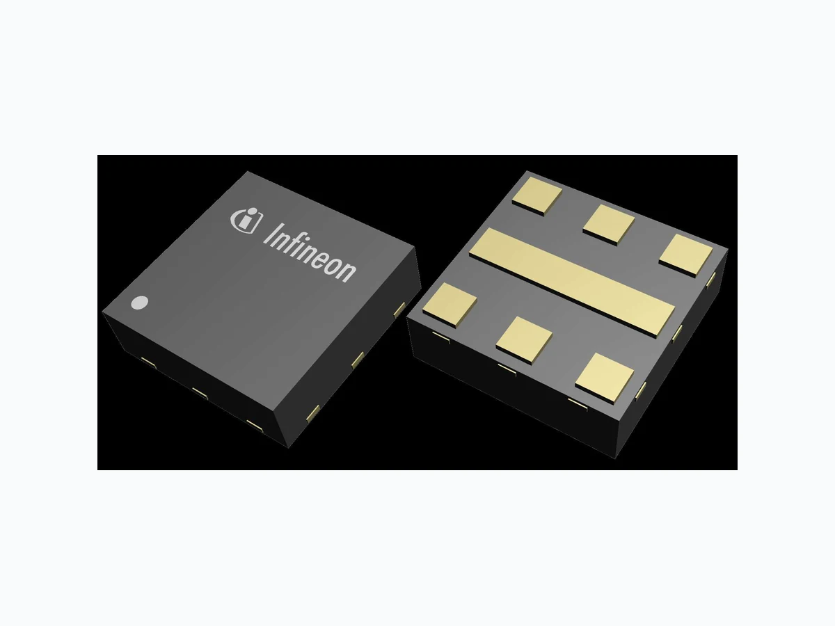
1EDN71X6U INFINEON
Document overview
- Manufacturer or author: Provided By digicamel.com
- PDF pages: 34
Technical content
Features
- Optimized for driving GaN SG HEMTs and Si MOSFETs
- Fully diferential logic input circuitry to avoid false triggering in low-side or high-side operation
- High common-mode input voltage range (CMR) up to ± 200 V for high side operation
- High immunity to common-mode voltage transitions (100 V/ns) for robust operation during fast switching
- Compatible with 3.3 V or 5 V input logic
- Four driving strength variants to optimize switching speed without external gate resistors - up to 2 A source/sink current capability
- Active bootstrap clamp to avoid bootstrap capacitor overcharging during dead-time
- Active Miller clamp with 5 A sink capability to avoid induced turn-on
- Qualified for industrial applications according to the relevant tests of JEDEC47/20/22
Description
The 1EDN71x6U is a single-channel gate-driver IC optimized for driving Infineon CoolGaN™ Schottky Gate HEMTs, as well as other GaN SG HEMTs and Si MOSFETs. This gate driver includes several key features that enable a high-performance system design with GaN SG HEMTs, including Truly Diferential Input, four driving strength options, active Miller clamp, and bootstrap voltage clamp. Potential applications
- Single channel: - Synchronous rectifier - Class-E resonant wireless power
- Half-bridge (2 x 1EDN71x6U): - DC-DC converter - BLDC/PMSM motor drive - Class-D audio amplifier - Class-D resonant wireless power Product portfolio Part number Peak source/sink current Input pulse blanking time Package 1EDN7116U 2.0 A 20 ns PG-TSNP-7 1EDN7126U 1.5 A 40 ns PG-TSNP-7 1EDN7136U 1.0 A 60 ns PG-TSNP-7 1EDN7146U 0.5 A 80 ns PG-TSNP-7 Datasheet Please read the sections "Important notice" and "Warnings" at the end of this document Rev. 2.0 www.infineon.com 2022-07-20
1EDN71x6U EiceDRIVER™
200 V high-side TDI gate driver IC for GaN SG HEMTs and MOSFETs
Datasheet 2 Rev. 2.0 2022-07-20
1 Pin configuration and description
Figure 1 Pin configuration 1EDN71X6U in PG-TSNP-7 package, top view Table 1 Pin definitions and functions Pin Name Function 1 VDD Gate drive supply. 2 IN+ Connected to PWM output of controller via 47 k Ω or 75 kΩ resistor. 3 IN- Connected to controller ground via 47 k Ω or 75 kΩ resistor. 4 VSS Return path for VDD and thermal dissipation pad.
5 BST Bootstrap diode anode connection point, when used as a low-side
driver in a half-bridge configuration. 6 OUT_SNK Low-impedance gate pull-down to VSS (including active Miller clamp). 7 OUT_SRC Low-impedance gate pull-up to VDD. 1EDN71x6U EiceDRIVER™ Datasheet 3 Rev. 2.0 2022-07-20
2 Product information
2.1 Functional description
The 1EDN71x6U is a single-channel gate-driver IC optimized for compatibility with Infineon CoolGaN™ SG HEMTs, as well as other GaN HEMTs and Silicon MOSFETs. Thanks to the truly diferential input feature, the gate driver output state is exclusively controlled by the voltage diference between the two inputs, independent of the driver’s reference (ground) potential as long as the common-mode voltage is below 150 V (static) and 200 V (dynamic). This eliminates the risk of false triggering due to ground bounce in low-side applications, while also allowing 1EDN71x6U to address even high-side applications. The product is equipped with several key features especially designed to enhance the performance of CoolGaN™ SG HEMTs:
- four driving strength variants to optimize switching speed without external gate resistors
- active bootstrap clamping to avoid overcharging the bootstrap capacitor during dead-time
- an active Miller clamp with exceptionally strong pull-down to avoid induced turn-on Figure 2 Typical circuit for low-side single-channel application using 1EDN71X6U to drive a CoolGaN™ SG HEMT
2.2 Truly diferential input (TDI)
The TDI feature ofers common-mode voltage rejection up to 150 V for static voltage and 200 V for dynamic voltage transients, enabling both low-side and high-side gate driving without the need for a digital isolator at the input. The dynamic voltage rating is relevant for any voltage spikes shorter than the specified blanking time (that is, minimum pulse width). When used as a low-side gate driver, the TDI greatly enhances ground bounce immunity during fast GaN switching transitions. At the positive and negative signal inputs two symmetrical resistor dividers are used to scale down and compensate common mode bouncing voltages. A fully diferential amplifier stage provides high common mode rejection and high sensitivity to diferential input signals. The amplified diferential output voltage is finally evaluated by the subsequent diferential Schmitt-Trigger circuit. At the IN+ and IN- pins, two external resistors Rin1 and Rin2 are used to scale down common mode voltages of up to ± 150 V to a level which can be processed by low voltage CMOS circuitry. These input resistors serve the function of "blocking" the high common-mode voltage, so that the IN+ and IN- pins of the driver are not exposed to this high voltage. As such, the selection of these resistors is critical to the proper operation of the TDI circuit. 1EDN71x6U EiceDRIVER™ Datasheet 4 Rev. 2.0 2022-07-20
Figure 3 Functional block diagram The resistance values for Rin1 and Rin2 must be selected based on the logic level of the input signals. For a 3.3 V logic, both external input resistors must be 47 kΩ. For a 5 V logic, they must be 75 kΩ. Furthermore, Rin1 and Rin2 must be very closely matched. A tolerance of ± 0.1 % is required to maintain control over the full common mode swing. Resistors with wider tolerance limit the common-mode range of the TDI driving circuit. Any asymmetries in these resistors may cause a a common-mode voltage to be interpreted as an input signal, including stray impedances in the PCB layout. Recommendations for a PCB layout are given later in this datasheet. To compensate for small asymmetries in the TDI circuit, low pass filters are used to further enhance the high frequency common mode rejection. Two diferent input filter options are available to accommodate diferent designs, with a total blanking time of 20 ns for 1EDN7116U, 40 ns for 1EDN7126U, 60 ns for 1EDN7136U, and 80 ns for 1EDN7146U.
2.3 Undervoltage lockout
The undervoltage lockout (UVLO) functions ensure that the output can be switched to its high level only if the VDD supply voltage exceeds the UVLO threshold voltage. The UVLO ensures that the transistors are not switched on if the driving voltage is too low, thereby avoiding excessive power dissipation due to linear-mode operation. The UVLO must be inactive to allow the propagation of the input control signals (IN+, IN-) to the output. The VDD UVLO level is set to a typical value of 3.85 V, with a maximum of 4.0 V. The maximum value of the rising edge is the value that ensures all the device among the production is turned on during start up. The designer must provide a voltage higher than 4.0 V to turn on all the devices in the production of their equipment within the specified temperature range. On the opposite side, the minimum voltage necessary to switch of all the devices is the minimum of the falling edge, which is 3.6 V. Therefore, a voltage lower than 3.6 V ensures that the driver does not start switching. Once the driver has exceeded the UVLO, the supply voltage must remain above the maximum falling edge level of 3.9 V to avoid a UVLO shutdown. The hysteresis is the voltage gap between rising edge and falling edge, which ensures some margin on noise efects such as false turn of. 1EDN71x6U EiceDRIVER™ Datasheet 5 Rev. 2.0 2022-07-20
The output states depend on the inputs configuration and the status of the VDD UVLO. The truth table of the driver is represented below. Table 2 Input logic truth table Diferential input UVLO VDD OUT_SNK OUT_SRC BST X ACTIVE HiZ HiZ HiZ L INACTIVE L HiZ L H INACTIVE HiZ H H Where:
- UVLO active means VDD < UVLOVDDL
- UVLO inactive means VDD > UVLOVDDH
- Diferential input = L means (V IN+ - VIN-) < input logic threshold
- Diferential input = H means (V IN+ - VIN-) > input logic threshold
2.4 Minimum input pulse
The minimum input pulse is the shortest duration pulse at the diferential input that will generate an output pulse. Pulses with durations shorter than the minimum pulse are neglected and therefore will not generate any output pulse. Once the input pulse has suficient duration to be propagated, the duration of the output pulse is equal to the duration of the input pulse, having therefore a linear transfer function between input and output. The minimum input pulse is specified here as "shortest input pulse transferred to the output. " The maximum value for this parameter is the pulse width at which all the drivers in production will provide an output signal. In other words, the designer must provide a pulse width longer than the maximum specified value to ensure an output pulse for every driver of their equipment. Likewise, any pulses shorter than the minimum specified value will be ignored by all drivers in production. This minimum specification can be treated as the guaranteed blanking time for de-glitching, which helps to prevent spurious switching during common-mode transient events.
2.5 Driver outputs
The output stage of the driver has a peak source and sink current as defined for the given product variant, which corresponds to an equivalent resistance of the pull-up and pull-down transistor. The designer can optimize the switching speed of the driven transistor by selecting one of the four product variants, without the need for external gate resistors. If external gate resistors are used, it is highly recommended to avoid placing a resistor in the output sinking path, as this limits the efectiveness of the active Miller clamp described in the next section. Source and sink outputs are actively held low with a clamp in case of floating inputs or during startup or power down. Under any situation, outputs are held under defined conditions to avoid unstable or unknown behavior of the driven transistor.
2.6 Active Miller clamp
The sink output of the gate driver has an active Miller clamp feature to provide high immunity to spurious turn-on events. During a turn-of transition, the peak sinking current and equivalent pull-down resistance is defined according to the product variant. However, once the driver detects that the gate voltage (at the sink output) has fallen below 0.4 V, the active Miller clamp is engaged within 3 ns, increasing the strength of the Sink output significantly. With the clamp engaged, all four product variants can sink up to 5 A, with an equivalent pull-down resistance of 0.3 Ω. This feature allows the designer to optimize the turn-of speed without sacrificing the driver's "keep-of" strength. If an external gate resistor is placed at the sink output, the efectiveness of the active Miller clamp is reduced. 1EDN71x6U EiceDRIVER™ Datasheet 6 Rev. 2.0 2022-07-20
2.7 Active bootstrap clamp
When using the bootstrapping technique to supply the high-side gate driver in a half-bridge topology, it is sometimes necessary to regulate the bootstrap capacitor voltage to avoid damaging the gate of the high-side transistor. This is especially important for GaN transistors for two reasons: 1. GaN SG HEMTs are oten sensitive to gate over-voltage, with driving voltages typically in the range of 5 V +/- 1 V. 2. The "body diode" mechanism of GaN transistors causes a higher voltage drop than MOSFETs, which leads to excessive over-charging of the bootstrap capacitor during dead-time conduction. In a half-bridge configuration, the bootstrap capacitor is normally charged during the low-side switch conduction time. Figure 4 shows this charging path, which includes the power supply (VDD), the bootstrap diode, current-limiting resistor, the bootstrap capacitor, and the low-side switch. When the low-side switching is turned fully on, the voltage applied to the bootstrap capacitor is slightly lower than VDD, due to the drop across the bootstrap diode, which can be partially compensated by the drop across the low-side transistor. However, during dead-time intervals, the low-side transistor operates in "body diode" mode, with a voltage drop in the range of 1.5 ~ 2.5 V, or even higher when a negative of-state VGS is applied. This causes over-charging of the bootstrap capacitor during the dead-time, resulting in a bootstrap voltage that varies significantly with dead-time duration and operating current, with a high risk of exceeding the maximum rated VGS of the driven transistor. This is not a problem for a typical MOSFET , since the operating range of the gate is fairly wide. However, this variable bootstrap capacitor voltage may pose a serious risk of damage to GaN Schottky gates. Therefore, it is necessary to apply some form of regulation to this circuit. For example, a Zener diode can be used as shown in Figure 4 , as long as the dead-time interval is well-controlled and paired with a current-limiting resistor that avoids overheating the Zener diode. The 1EDN71X6U driver ofers an alternative bootstrap clamping scheme. Figure 5 shows the implementation of this bootstrap clamping scheme in a half-bridge circuit. The clamp circuit avoids over-charging the bootstrap capacitor instead of directly regulating the capacitor voltage, which would likely contribute additional losses. Rather than connecting the bootstrap diode to the VDD supply rail, it is connected to the BST output of the low-side driver. The BST output operates as a clone of the source and sink output pins, synchronized to the timing of the low-side transistor turning on and of. Therefore, the bootstrap diode can only conduct current when the low-side transistor is turned fully on, but not when it is operating in "body diode" mode during dead-time. The active bootstrap clamping scheme is very useful in regulating the high-side driving voltage without the need for additional components. However, in applications where over-charging of the bootstrap capacitor is desired, the bootstrap diode can be connected to the VDD pin instead of the BST pin. A Zener-based regulation scheme is recommended in this case, as shown in Figure 4. 1EDN71x6U EiceDRIVER™ Datasheet 7 Rev. 2.0 2022-07-20
Figure 4 Half-bridge with Zener bootstrap regulation 1EDN71x6U EiceDRIVER™ Datasheet 8 Rev. 2.0 2022-07-20
Figure 5 Half-bridge with active bootstrap clamping
2.8 Unpowered gate clamp
The unpowered gate clamp circuit ensures that the driver output is pulled low when no supply voltage is applied to the driver. It is common practice to place a resistor between the gate and source of transistors to ensure that there is no spurious voltage when the system is powered of. However, this is not necessary with the 1EDN71x6U. The driver has an internal pull-down MOSFET between the OUT_SNK pin and VSS pin, which pulls down the gate voltage to VSS with a peak current capability of 3 mA, whenever VDD is not suficiently supplied to turn on the driver. Once the 1EDN71x6U is fully powered on, this pull-down MOSFET is disabled. OUT_SNK Power_on VSS Figure 6 Functional diagram of unpowered gate clamp circuit 1EDN71x6U EiceDRIVER™ Datasheet 9 Rev. 2.0 2022-07-20
3 General product characteristics
3.1 Absolute maximum ratings
All voltages are referred to VSS unless otherwise specified. Table 3 Absolute maximum ratings Parameter Symbol Values Unit Note or condition Min. Typ. Max. Driver supply VDD -0.3 – 12 V Driver supply, transient VDD – – 13.2 V < 3 ns Voltage at IN+ pin VIN+ -8.5 – 8.5 V Voltage at IN- pin VIN- -8.5 – 8.5 V Voltage at OUT_SRC, OUT_SNK, BST pins VOUT_SRC, VOUT_SNK, VBST -0.3 - VDD + 0.3 V Junction temperature TJ -40 – 150 oC Storage temperature TS -55 – 150 oC Soldering temperature – – 260 oC
3.2 Recommended operating conditions
The following operating conditions must not be exceeded to ensure correct operation and reliability of the device. All parameters specified in the following tables refer to these operating conditions, unless noted otherwise. Table 4 Recommended operating conditions Parameter Symbol Values Unit Note or condition Min. Typ. Max. Supply voltage VDD 4.2 – 11 V Operating frequency FSW – – 15 MHz Common mode voltage range (static) CMR -150 – 150 V Rext = 47k ± 0.1%, Vlogic = 3.3 V. (table continues...) 1 Verified by design/characterization. Not subject to production test. 1EDN71x6U EiceDRIVER™ Datasheet 10 Rev. 2.0 2022-07-20
Table 4 (continued) Recommended operating conditions Parameter Symbol Values Unit Note or condition Min. Typ. Max. Common mode voltage range (dynamic) CMRdyn -200 – 200 V Rext = 47k ± 0.1%, Vlogic = 3.3 V. Duration of voltage transient event must be shorter than specified blanking time. Common mode voltage slew rate CMSR – – 100 V/ns
3.3 ESD ratings
Symbol Description Value Unit ESDHBM Human Body Model sensitivity as per ANSI/ESDA/JEDEC JS-001 1500 V ESDCDM Charged Device Model sensitivity as per ANSI/ESDA/JEDEC JS-002 1000 V
3.4 Thermal resistance
Table 6 Thermal resistance Parameter Symbol Values Unit Note or condition Min. Typ. Max. Junction-to- ambient thermal resistance RthJA – 80 – °C/W JEDEC 2s2p with thermal vias. Junction-to- case thermal resistance - bottom RthJC(BOT) – 28 – °C/W Junction-to- case thermal resistance - top RthJC(TOP) – 114 – °C/W 1 Verified by design/characterization. Not subject to production test. 2 Obtained in a simulation on a JEDEC-standard 2s2p four-layer PCB with thermal vias, as specified in JESD51-7, in an environment described in JESD51-2a. 1EDN71x6U EiceDRIVER™ Datasheet 11 Rev. 2.0 2022-07-20
3.5 Static electrical characteristics
VDD - VSS = 5 V, Tc = - 40oC to 125ºC unless otherwise specified. Table 7 Static electrical characteristics Parameter Symbol Values Unit Note or condition Min. Typ. Max. Undervoltage lockout thresholds VDD supply UVLO rising threshold UVLOVDDH 3.7 3.85 4 V VDD supply UVLO falling threshold UVLOVDDL 3.6 3.75 3.9 V Current consumption VDD quiescent current IQDD – – 1.8 mA IN+ = IN- = 0 V. VDD current consumption when switching IODD – – 2.6 mA fSW = 500 kHz, no load on OUT_SRC/ OUT_SNK and no load on BST . Apply PWM to IN+, set IN- = 0 V. Common mode = 0 V. Input characteristics Diferential input voltage threshold for low-high transition ΔVRinH 1.7 1.95 2.2 V Thresholds valid for REXT = 47 kΩ. VCM = 0 V and T = 25 ºC. Diferential input voltage threshold for low-high transition ΔVRinH 1.2 1.95 2.65 V Thresholds valid for REXT = 47 kΩ. VCM = -150 V to 150 V. Diferential input voltage threshold for high-low transition ΔVRinL 1.1 1.35 1.6 V Thresholds valid for REXT = 47 kΩ. VCM = 0 V and T = 25 ºC. Diferential input voltage threshold for high-low transition ΔVRinL 0.7 1.35 2.15 V Thresholds valid for REXT = 47 kΩ. VCM = -150 V to 150 V. 1EDN71x6U EiceDRIVER™ Datasheet 12 Rev. 2.0 2022-07-20
3.6 Driver output characteristics
Table 8 Driver output characteristics Parameter Symbol Typical values Unit Note or condition1EDN7116U 1EDN7126U 1EDN7136U 1EDN7146U Peak source current IOUT_SRC 2 1.5 1 0.5 A VDD = 5 V, OUT_SRC = 0 V 1) Peak sink current IOUT_SNK 2 1.5 1 0.5 A VDD = 5 V, OUT_SNK = 5 V 1) Peak sink current w/ Miller clamp IOUT_SNK _MC 5 5 5 5 A VDD = 5 V, OUT_SNK = 5 V 1) Pull-up resistance RPU 0.8 1.1 1.6 3.3 Ω I_SRC = 100 mA Pull-down resistance RPD 0.7 1.0 1.5 3.0 Ω I_SNK = 100 mA Pull-down resistance w/ Miller clamp RPD_MC 0.3 0.3 0.3 0.3 Ω I_SNK = 100 mA Active Miller clamp voltage threshold VMC_TH 0.4 0.4 0.4 0.4 V 1) Active Miller clamp propagation delay TMCD 3 3 3 3 ns No load. 1) Unpowered gate clamp sinking current IOUT_SNK _UGC 3 3 3 3 mA VDD floating. 1.2 V applied externally to OUT_SNK. Rise time TR 3 4 5.5 11 ns OUT_SRC and OUT_SNK shorted. CL = 1 nF, VDD = 5 V 1) Fall time TF 3 4 5.5 11 ns BST peak source current IBST_SRC 2 2 2 2 A VDD = 5 V, BST = 0 V 1) BST peak sink current IBST_SNK 2 2 2 2 A VDD = 5 V, BST = 5 V 1) BST pull-up resistance RBST_PU 0.8 0.8 0.8 0.8 Ω I_BST_SRC = 100 mA BST pull-down resistance RBST_PD 0.7 0.7 0.7 0.7 Ω I_BST_SNK = 100 mA 1) Verified by design/characterization. Not subject to production test. 1EDN71x6U EiceDRIVER™ Datasheet 13 Rev. 2.0 2022-07-20
3.7 Timing characteristics
Timings are obtained considering OUT_SRC and OUT_SNK shorted together, CLOAD = 0 nF and over common mode range -150 V to 150 V, VDD = 5 V, REXT = 47 kΩ unless specified otherwise. Table 9 Timing characteristics Parameter Symbol Values Unit Note or condition Min. Typ. Max. Startup time, ater UVLO threshold is reached tST 12 20 μs VSS = 0 V, Tj = 25oC. Turn-on propagation delay matching OUT to BST ΔTLH_BST -2 – 2 ns Calculated as TLH - TLH BST . VCM = 0 V, Tj = 25ºC. Turn-of propagation delay matching OUT to BST ΔTHL_BST -2 – 2 ns Calculated as THL - THL BST . VCM = 0 V, Tj = 25ºC. 1EDN7116U Turn-on propagation delay TLH 53 55 57 ns VCM = 0 V, Tj = 25ºC. Turn-of propagation delay THL 53 55 57 ns VCM = 0 V, Tj = 25ºC. Propagation delay matching ΔTLH_HL -2.2 0 2.2 ns Calculated as TLH - THL. VCM = 0 V, Tj = 25ºC. Shortest input pulse transferred to the output TPW_MIN 20 – 25 ns VCM = 0 V, Tj = 25ºC. 1EDN7126U Turn-on propagation delay TLH 73 75 77 ns VCM = 0 V, Tj = 25ºC. Turn-of propagation delay THL 73 75 77 ns VCM = 0 V, Tj = 25ºC. (table continues...) 1EDN71x6U EiceDRIVER™ Datasheet 14 Rev. 2.0 2022-07-20
Table 9 (continued) Timing characteristics Parameter Symbol Values Unit Note or condition Min. Typ. Max. Propagation delay matching ΔTLH_HL -2.8 – 2.8 ns Calculated as TLH - THL. VCM = 0 V, Tj = 25ºC. Shortest input pulse transferred to the output TPW_MIN 40 – 47 ns VCM = 0 V, Tj = 25ºC. 1EDN7136U Turn-on propagation delay TLH 101 105 109 ns VCM = 0 V, Tj = 25ºC. Turn-of propagation delay THL 101 105 109 ns VCM = 0 V, Tj = 25ºC. Propagation delay matching ΔTLH_HL -3.4 – 3.4 ns Calculated as TLH - THL. VCM = 0 V, Tj = 25ºC. Shortest input pulse transferred to the output TPW_MIN 60 – 71 ns VCM = 0 V, Tj = 25ºC. 1EDN7146U Turn-on propagation delay TLH 121 125 129 ns VCM = 0 V, Tj = 25ºC. Turn-of propagation delay THL 121 125 129 ns VCM = 0 V, Tj = 25ºC. Propagation delay matching ΔTLH_HL -3.8 – 3.8 ns Calculated as TLH - THL. VCM = 0 V, Tj = 25ºC. Shortest input pulse transferred to the output TPW_MIN 80 – 93 ns VCM = 0 V, Tj = 25ºC. 1EDN71x6U EiceDRIVER™ Datasheet 15 Rev. 2.0 2022-07-20
4 Typical characteristics
Figure 7 Diferential input voltage threshold versus temperature Figure 8 Diferential input voltage threshold versus common mode voltage 1EDN71x6U EiceDRIVER™ Datasheet 16 Rev. 2.0 2022-07-20
Figure 9 Quiescent current versus temperature Figure 10 Quiescent current versus supply voltage 1EDN71x6U EiceDRIVER™ Datasheet 17 Rev. 2.0 2022-07-20
Figure 11 Operating current with load versus frequency Figure 12 Turn-on propagation delay versus temperature 1EDN71x6U EiceDRIVER™ Datasheet 18 Rev. 2.0 2022-07-20
Figure 13 Turn-of propagation delay versus temperature Figure 14 Turn-on propagation delay versus common mode voltage 1EDN71x6U EiceDRIVER™ Datasheet 19 Rev. 2.0 2022-07-20
Figure 15 Turn-of propagation delay versus common mode voltage Figure 16 OUT_SRC pull-up resistance versus temperature 1EDN71x6U EiceDRIVER™ Datasheet 20 Rev. 2.0 2022-07-20
Figure 17 OUT_SNK pull-down resistance versus temperature (before active Miller clamp is engaged) Figure 18 OUT_SNK pull-down resistance versus temperature (ater Miller clamp is engaged) 1EDN71x6U EiceDRIVER™ Datasheet 21 Rev. 2.0 2022-07-20
Figure 19 BST pull-up and pull-down resistance versus temperature Figure 20 Undervoltage lockout threshold versus temperature 1EDN71x6U EiceDRIVER™ Datasheet 22 Rev. 2.0 2022-07-20
Figure 21 Shortest input pulse transferred to output versus temperature 1EDN71x6U EiceDRIVER™ Datasheet 23 Rev. 2.0 2022-07-20
5 Application information
5.1 Typical application circuits
The 1EDN71x6U can be used as a single low-side driver or a single high-side driver, and two can be used together to drive a half-bridge. Figure 22 depicts an example circuit schematic for a single-device driver. Figure 4 and Figure 5 show two examples of half-bridge circuit schematics with two 1EDN71x6U, with conventional bootstrapping and Zener regulation in the first, and active bootstrap clamping enabled in the second. Figure 23 shows an additional example of half-bridge implementation, in this case with cross-connected PWM inputs for the high-side and low-side drivers. This option adds robustness against accidental cross-conduction in case the controller ever generates overlapping PWM signal. However, it may also limit the minimum dead-time as measured at the gate signals of the driven devices, due to asymmetrical turn-on and turn-of delay times of the driven transistors. Figure 22 Single channel application circuit 1EDN71x6U EiceDRIVER™ Datasheet 24 Rev. 2.0 2022-07-20
Figure 23 Half-bridge with cross-connected signal inputs and active bootstrap clamping Figure 24 TDI application circuit, including input external resistors and stray capacitance 1EDN71x6U EiceDRIVER™ Datasheet 25 Rev. 2.0 2022-07-20
5.2 Selection of TDI input resistors
The 1EDN71X6U requires precise input resistors at the IN+ and IN- pins, with resistance values of 47 kΩ or 75 kΩ, depending on the voltage level of the input logic signals. The driver is compatible with either a 3.3 V or a 5 V logic. These resistors are not optional, even if the application does not require the TDI function (for example low-side applications with no ground bounce concerns). The input logic thresholds at the IN+ and IN- pins are designed to be paired with the specified input resistor values. These input resistors should be selected with a 0.1% tolerance, especially in high-side applications, where the common-mode voltage rating is contingent upon tight matching of RIN1 and RIN1. Extra care should be taken to ensure that these resistors are symmetrical, so that stray capacitance across them is also tightly matched. Figure 24 shows an example of how stray capacitances Cp1 and Cp2 could interfere with the symmetry and matching of RIN1 and RIN2. To optimize this symmetry, the two resistors should have identical part numbers with the same package and footprint. Further PCB layout recommendations for ensuring symmetry are given later. In high-side applications, the input resistors must also be rated for the power dissipation expected in the worst-case operating conditions. The common-mode voltage observed by the high-side transistor is "blocked" by each input resistor, so that the 1EDN71X6U is not exposed to the high voltage. The resistors dissipate power during the intervals where CM voltage is high, typically during the high-side transistor's duty ratio of each switching period. The power rating of the resistors should therefore be selected based on PRin1 = PRin2 = Vdc, max Rin1 × D Equation 1 where: PRin1 = Required power rating for Rin1 PRin2 = Required power rating for Rin2 D = High-side duty ratio Vdc,max = Maximum expected dc bus voltage, experienced as CM voltage during the high-side duty ratio It is important to consider that the duty ratio may not be constant, so D should be selected as the duty ratio when operating at the maximum dc bus voltage. The table below lists some examples for selecting the input resistors, based on logic voltage level, expected dc bus voltage, and duty ratio. For most applications, the power requirement is quite low, thereby allowing the designer to select very small resistor packages such as 0402 or 0603. In some extreme scenarios with a high dc voltage and high duty ratio simultaneously, larger packages with higher power ratings may be needed. Table 10 Examples for selected input resistors Maximum dc bus voltage Logic voltage Duty ratio TDI input resistance Resistor tolerance Minimum Rin power rating 60 V 3.3 V 0.25 47 k Ω 0.1% 0.02 W 60 V 5 V 0.25 75 k Ω 0.1% 0.01 W 80 V 3.3 V 0.75 47 k Ω 0.1% 0.10 W 80 V 5 V 0.75 75 k Ω 0.1% 0.06 W
5.3 Selection of VDD bypass capacitor
The VDD bypass capacitor provides the gate charge to drive the transistor, as well as additional power consumption by the driver itself. It should be placed as close as possible to the VDD and VSS pins of the gate driver, which may require a particular footprint size for most applications. The minimum value for this bypass capacitor can be calculated based on the maximum allowable voltage ripple in the design. This ripple should be minimized such that the lowest possible VDD is above the UVLO limit of the gate driver as well as above the safe driving voltage of the transistor. The charge dissipated per 1EDN71x6U EiceDRIVER™ Datasheet 26 Rev. 2.0 2022-07-20
switching event is approximately equal to the driven transistor's gate charge. The minimum value can therefore be calculated as CVdd ≫ QG ∆VDD, max Equation 2 In a half-bridge configuration, the VDD bypass capacitor also provides the charge for the bootstrap capacitor during the charging period. Therefore, the VDD bypass capacitor should be sized to be much larger than the bootstrap capacitor. The minimum value should be calculated as CVdd ≫ QG + QBOOT ∆VDD, max Equation 3 where QBOOT is the charge consumed by the bootstrapping circuit each cycle. This value is calculated in a later section. In practice, this capacitance value should be increased somewhat to account for dc bias efects in the capacitor and other non-idealities in the circuit.
5.4 Selection of external bootstrap diode
When used in a half-bridge configuration, a bootstrapping circuit is oten used to supply the high-side driver's VDD. A fast recovery or schottky diode with low forward voltage drop is recommended in order to minimize the losses and leakage current. It should be chosen such that it can handle the peak transient current during start-up conditions and the blocking voltage rating should be higher than the maximum input voltage (VIN) with added margin. It is important to consider that the output capacitance and reverse recovery of this bootstrap diode contributes to the total switch-node capacitance of the half-bridge, thereby increasing the total switching losses of the application circuit. A schottky diode with low output capacitance is therefore the best choice for most applications. The 1EDN71x6U gate driver provides two options for bootstrap diode connection. The conventional approach is to connect the anode of the diode to the low-side VDD rail, oten with a current-limiting resistor between them to limit surge current during startup. However, the recommended approach with 1EDN71x6U is to connect the anode of the bootstrap diode to the BST pin of the low-side driver as shown in Figure 4 . This enables the integrated bootstrap clamping function of the driver, and it also provides current-limiting at startup without the need for an added resistor.
5.5 Selection of bootstrap capacitor
The bootstrap capacitor provides the necessary charge to drive the high-side transistor. It must be sized in such a way that its lowest voltage will be much higher than the UVLO threshold as well as above the minimum safe driving voltage of the transistor, during transient and normal operations. To determine the minimum required bootstrap capacitance, the maximum allowable ripple in VBOOT must be calculated as follows. ∆VBOOT, max = VDD − VF − VBOOT, min Equation 4 where: VDD = Low-side gate driver supply voltage VF = Bootstrap diode forward voltage drop 1EDN71x6U EiceDRIVER™ Datasheet 27 Rev. 2.0 2022-07-20
VBOOT ,min is the minimum allowable voltage for the bootstrap capacitor, including transient events. This voltage must be at least high enough to avoid UVLO shutdown, as given by: VBOOT, min ≥ VHBR + VHBH Equation 5 where: VHBR = High-side driver UVLO rising threshold VHBH = High-side driver UVLO threshold hysteresis However, the driven transistor may require a higher voltage than this UVLO minimum, in order to remain fully on and avoid linear-mode operation. If the calculated minimum VBOOT is lower than the safe driving voltage of the transistor, then VBOOT ,min should be increased accordingly. Next, determine the total charge (QBOOT) that must be delivered by the bootstrap capacitor at maximum duty cycle. There are several factors that contribute to the discharge of the bootstrap capacitor such as the high-side transistor’s total gate charge and gate-source leakage current, bootstrap diode reverse bias leakage current, and bootstrap capacitor leakage current. For the sake of simplicity, the bootstrap capacitor leakage current can typically be neglected. The total bootstrap charge can be estimated as follows: QBOOT ≈ QG + IVdd + Idiode × Dmax fsw Equation 6 where: QG = High-side transistor total gate charge IVdd = High-side driver maximum quiescent current Idiode = Bootstrap diode reverse bias leakage current Dmax = Maximum high-side duty cycle fsw = Switching frequency The minimum bootstrap capacitor value can then be calculated using the formula: CBOOT ≫ QBOOT ∆ VBOOT, max Equation 7 In practice, this capacitance value should be increased somewhat to account for dc bias efects in the capacitor and other non-idealities in the circuit.
5.6 Selection of external gate resistors
The turn-on and turn-of external gate resistors control the turn-on and turn-of current of the gate driver providing an external way to control the switching speed of the MOSFET for purposes such as voltage overshoot control, ringing reduction, EMI mitigation, spurious turn-on protection, shoot –through protection, etc. In most designs, no external gate resistor is needed. Each of the four product variants ofers a diferent pull-up and pull-down resistance, along with a corresponding peak source and sink current. However, in cases where the designers prefers a diferent source and sink driving strength, an external gate resistor may be used. The following formulas show the efect of the external gate resistor to the output current capability of the gate driver. ISRC, PK≤ VDD RPU + RG, int+ RGon, ext Equation 8 1EDN71x6U EiceDRIVER™ Datasheet 28 Rev. 2.0 2022-07-20
ISNK, PK ≤ VDD RPD + RG, int+ RGoff, ext Equation 9 where: ISRC,PK = Peak source current ISNK,PK = Peak sink current RPU = Gate driver pull-up resistance RPD = Gate driver pull-down resistance VDD = Gate driver supply voltage (equivalent to VBOOT for high-side transistor) RG,int = Internal gate resistance of driven transistor RGon,ext = External gate resistance connected between Source output and gate RGof,ext = External gate resistance connected between Sink output and gate It is important to consider that the peak current may not reach this level during a fast switching transition, as is typical with GaN transistors. It is also worth nothing that this peak current cannot exceed the specified peak source/sink current of the gate driver, as the pull-up and pull-down transistors within the driver saturate at that current. However, the selection of product variant according to pull-up and pull-down resistance provides a close approximation to selection of external gate resistance in most cases. Use of a non-zero RGof_ext is not recommended for most designs, as this limits the efectiveness of the active Miller clamp feature. It is therefore preferable to choose the product variant based on the desired sinking or pull-down strength, and then add RGon_ext only if needed to optimize the design.
5.7 PCB layout recommendations
The combination of the gate driver, bypass capacitors, and driven transistor forms a high-frequency current loop that defines the parasitic inductance in series with that loop. Likewise, in a half-bridge, the combination of the high-side and low-side transistors forms a high-frequency current loop with the bypass capacitors for the dc bus (for example Vin for a buck converter). The relative location on the PCB of those components is essential to reach high level of performance. The parasitic inductances within these loops can cause serious eficiency degradation due to dynamic efects. In addition, any coupling between the gate driving loops and half-bridge power loop can cause spurious switching events or other performance degradation. Coupling between either of these loops and the signal paths feeding to the TDI input resistors can also cause spurious switching. Finally, as mentioned previously, the TDI input circuit may be afected by stray capacitance and other asymmetries in the PCB design. Careful layout can help minimize or eliminate such unwanted efects. The following recommendations help the designer to optimize the PCB layout, as demonstrated in the half- bridge example pictures below. 1. Keep all high-frequency loops as short as possible, and use diferential returns for current paths to cancel the magnetic fields and reduce parasitic inductance. 2. Minimize stray inductance, especially on low impedance lines. All high-current traces (VDD, VSS, OUT_SRC, OUT_SNK) should be short and wide, and copper pours are recommended over traces when the design allows. 3. To optimize heat spreading, electrical shielding, and magnetic field cancellation, a VSS-connected copper pour should be placed directly underneath the IC as well as all components encompassed by the gate driving loop (for example bypass capacitors, gate and source pads of transistor). For the low-side driver, this shielding pour should be connected to PGND. For the high-side driver, it should be connected to the switch-node, which is the mid-point of the half-bridge. 4. To avoid interference between the power loop and gate loops, separate shielding layers should be used for each loop, even if they are both connected to the same net. 5. To optimize the symmetry of the TDI input resistors, they should be placed directly beside each other and symmetrically shielded on the first inner layer. The controller-side of the two resistors should be 1EDN71x6U EiceDRIVER™ Datasheet 29 Rev. 2.0 2022-07-20
shielded by the controller ground net (SGND), and the driver-side of the two resistors should be shielded by the same VSS-connected copper used to shield the rest of the driving circuit. 6. The dielectric spacing between the top copper layer and first inner layer should be minimized to enhance the magnetic field cancellation efects. A spacing of 80 ~ 100 microns is used in the example below. Figure 25 3D top-side view of example half-bridge implementation 1EDN71x6U EiceDRIVER™ Datasheet 30 Rev. 2.0 2022-07-20
Figure 26 Top copper layer of example half-bridge implementation Figure 27 First inner layer of example half-bridge implementation, separated from top layer by 80~100 µm dielectric 1EDN71x6U EiceDRIVER™ Datasheet 31 Rev. 2.0 2022-07-20
6 Package information
Package type From Quantity Orderable part number Marking code 1EDN7116U PG-TSNP-7-11 Tape and reel 4500 1EDN7116UXTSA1 1EDN7116U 1EDN7126U PG-TSNP-7-11 Tape and reel 4500 1EDN7126UXTSA1 1EDN7126U 1EDN7136U PG-TSNP-7-11 Tape and reel 4500 1EDN7136UXTSA1 1EDN7136U 1EDN7146U PG-TSNP-7-11 Tape and reel 4500 1EDN7146UXTSA1 1EDN7146U Figure 28 PG-TSNP-7-11 packaging 1EDN71x6U EiceDRIVER™ Datasheet 32 Rev. 2.0 2022-07-20
Figure 29 PG-TSNP-7-11 package dimensions Figure 30 PG-TSNP-7-11 recommended landing pattern 1EDN71x6U EiceDRIVER™ Datasheet 33 Rev. 2.0 2022-07-20
200Vhigh-sideTDIgatedriverICforGaNSGHEMTsandMOSFETs 1EDN71x6U Rev.2.0,2022-07-29 RevisionHistory 1EDN71x6U Revision:2022-07-29,Rev.2.0 Previous Revision Revision Date Subjects (major changes since last revision) 2.0 2022-07-29 Release of final version Trademarks Allreferencedproductorservicenamesandtrademarksarethepropertyoftheirrespectiveowners. WeListentoYourComments Anyinformationwithinthisdocumentthatyoufeeliswrong,unclearormissingatall?Yourfeedbackwillhelpustocontinuously improvethequalityofthisdocument.Pleasesendyourproposal(includingareferencetothisdocument)to: erratum@infineon.com Publishedby InfineonTechnologiesAG 81726München,Germany ©2022InfineonTechnologiesAG AllRightsReserved. LegalDisclaimer Theinformationgiveninthisdocumentshallinnoeventberegardedasaguaranteeofconditionsorcharacteristics (“Beschaffenheitsgarantie”). Withrespecttoanyexamples,hintsoranytypicalvaluesstatedhereinand/oranyinformationregardingtheapplicationofthe product,InfineonTechnologiesherebydisclaimsanyandallwarrantiesandliabilitiesofanykind,includingwithoutlimitation warrantiesofnon-infringementofintellectualpropertyrightsofanythirdparty. Inaddition,anyinformationgiveninthisdocumentissubjecttocustomer’scompliancewithitsobligationsstatedinthis documentandanyapplicablelegalrequirements,normsandstandardsconcerningcustomer’sproductsandanyuseofthe productofInfineonTechnologiesincustomer’sapplications. Thedatacontainedinthisdocumentisexclusivelyintendedfortechnicallytrainedstaff.Itistheresponsibilityofcustomer’s technicaldepartmentstoevaluatethesuitabilityoftheproductfortheintendedapplicationandthecompletenessoftheproduct informationgiveninthisdocumentwithrespecttosuchapplication. Information Forfurtherinformationontechnology,deliverytermsandconditionsandpricespleasecontactyournearestInfineon TechnologiesOffice(www.infineon.com). Warnings Duetotechnicalrequirements,componentsmaycontaindangeroussubstances.Forinformationonthetypesinquestion, pleasecontactthenearestInfineonTechnologiesOffice. TheInfineonTechnologiescomponentdescribedinthisDataSheetmaybeusedinlife-supportdevicesorsystemsand/or automotive,aviationandaerospaceapplicationsorsystemsonlywiththeexpresswrittenapprovalofInfineonTechnologies,ifa failureofsuchcomponentscanreasonablybeexpectedtocausethefailureofthatlife-support,automotive,aviationand aerospacedeviceorsystemortoaffectthesafetyoreffectivenessofthatdeviceorsystem.Lifesupportdevicesorsystemsare intendedtobeimplantedinthehumanbodyortosupportand/ormaintainandsustainand/orprotecthumanlife.Iftheyfail,itis reasonabletoassumethatthehealthoftheuserorotherpersonsmaybeendangered.