
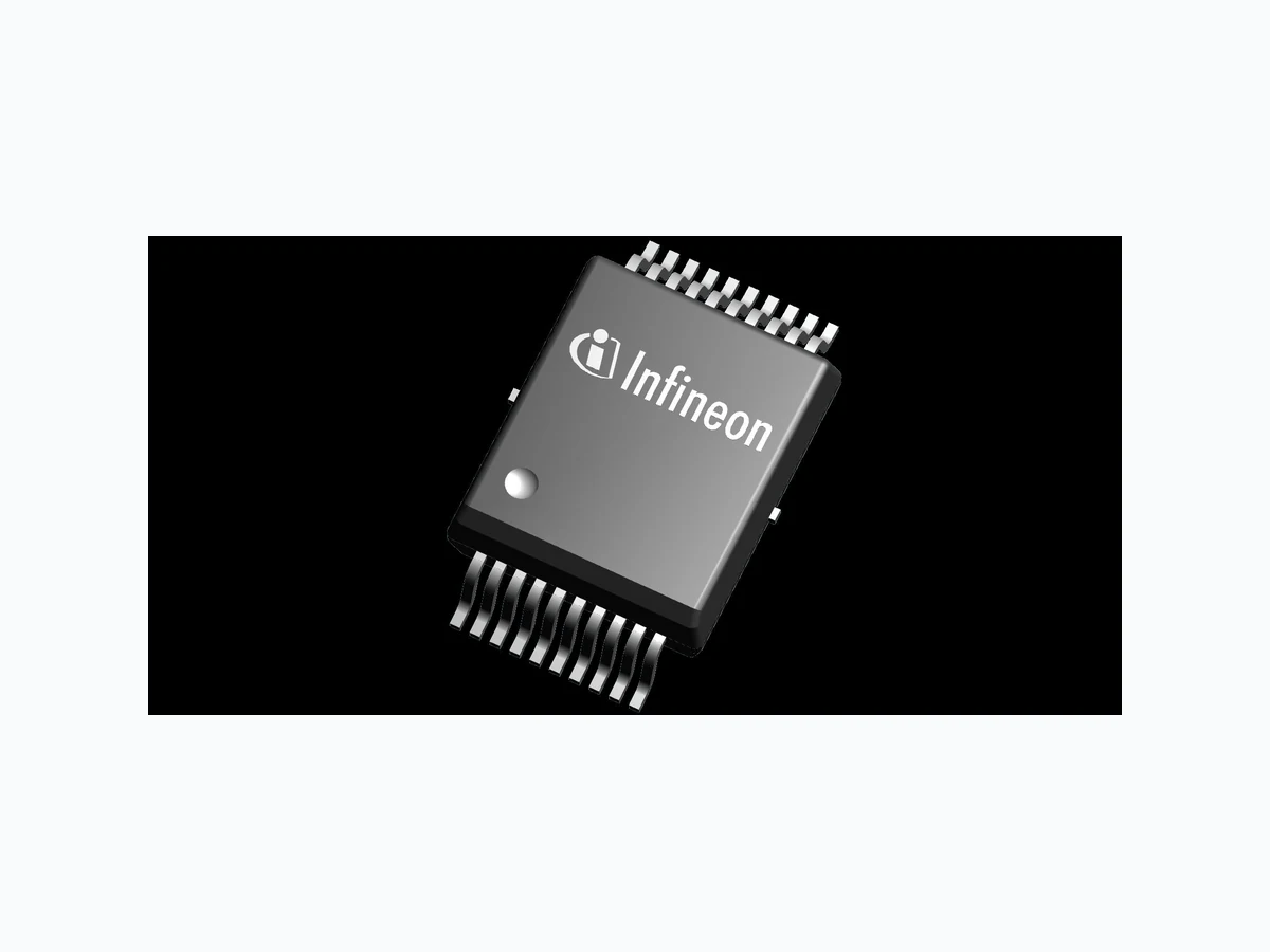
1EDI3038AS INFINEON
Document overview
- Manufacturer or author: Provided By digicamel.com
- PDF pages: 70
Technical content
Features
- Galvanic isolated SiC-MOSFET driver using coreless transformer technology
- Single channel driver for SiC-MOSFETs up to 1200 V
- Low propagation delay 60 ns typically
- Split outputs TON and TOFF for independent turn-on and turn-off slew rates
- Integrated booster with up to 15 A peak current rail-to-rail output
- Integrated active Miller clamp supports unipolar switching
- Configurable external soft turn-off functionality
- CMTI up to 150 V/ns up to ±1200 V
- Reinforced insulation 8 kV peak according to DIN EN IEC 60747-17 - Safety pins on primary side and secondary ASC - Super fast DESAT including BIST - Gate monitoring and output stage monitoring - Shoot-through protection with integrated timeout - Primary supply monitoring UVLO - Secondary supply monitoring VCC2 for OVLO and UVLO, VEE2 for UVLO only
- DATA interface for detailed error diagnosis via PWM signal
- 3.3 V and 5 V compatible I/O logic supply
- ISO 26262 Safety Element out of Context for safety requirements up to ASIL B
- Green Product (RoHS compliant) (VDE 0884-17):2021-10
- 5.7 kV rms insulation according to UL 1577
- Secondary side active short circuit (SASC) pin
- Integrated safety features up to ASIL B: Potential applications
- Traction inverters for HEV and EV
- Auxiliary inverters for HEV and EV
- High power and fail save on-board chargers for HEV and EV
- High power and fail save DC/DC converters Product validation Qualified for automotive applications. Product validation according to AEC-Q100. Datasheet Please read the sections "Important notice" and "Warnings" at the end of this document Rev. 1.0 www.infineon.com/isolated-high-voltage-gate-driver 2024-06-20
Description
The EiceDRIVER™ gate driver 1EDI3038AS is a high voltage galvanic isolated SiC-MOSFET driver designed for high voltage automotive applications. The device is based on Infineon’s coreless transformer (CT) technology providing 8 kV galvanic insulation between low voltage and high voltage domains. The IC supports up to 1200 V SiC-MOSFETs. The device features a powerful output stage of up to 15 A peak current required for high power switches. A split output stage (TON, TOFF) allows different slew rates for switching on and switching off due to separate gate resistors. The low voltage domain (primary side) supports logic levels of 5 V as well as 3.3 V. At the high voltage domain (secondary side) it can drive the gate of SiC-MOSFETs directly. A short propagation delay of only 60 ns and a minimum pulse width of 150 ns offer high a switching frequency with minimum distortion of the PWM signal. The DESAT protection together with the configurable external soft turn-off feature prevents SiC-MOSFETs destruction in short-circuit events. The integrated active Miller clamping stage up to 10 A allows unipolar supply of the SiC-MOSFET. The device features a DATA interface that provides detailed error diagnosis through a PWM signal. A large panel of integrated safety related features simplifies the design of ASIL D compliant systems. Safety inputs (SI1, SI2) at the primary side control the transition of the system to safe state. Additionally, the device offers a secondary side active short circuit (ASC) pin to trigger safe state also from the secondary side. Type Package Marking 1EDI3038AS PG-DSO-20 1EDI3038AS EiceDRIVER™ gate driver 1EDI3038AS Single channel isolated SiC-MOSFET driver Datasheet 2 Rev. 1.0 2024-06-20
EiceDRIVER™ gate driver 1EDI3038AS Single channel isolated SiC-MOSFET driver Table of contents Datasheet 3 Rev. 1.0 2024-06-20
EiceDRIVER™ gate driver 1EDI3038AS Single channel isolated SiC-MOSFET driver Table of contents Datasheet 4 Rev. 1.0 2024-06-20
EiceDRIVER™ gate driver 1EDI3038AS Single channel isolated SiC-MOSFET driver Table of contents Datasheet 5 Rev. 1.0 2024-06-20
1 Block diagram
Control & Monitoring VCC2 TON GND1 P-Supply UVLO1 NFLT GND1 INP TOFF PWM Input Stage GND2 P-Supply UVLO2 OVLO2 UVLO3 SOFTOFF ASC SASC DESAT GATE/CLAMP Figure 1 Block diagram EiceDRIVER™ gate driver 1EDI3038AS Single channel isolated SiC-MOSFET driver Datasheet 6 Rev. 1.0 2024-06-20
2 Pin configuration
1 GND1
2 VCC1
3 DATA
4 NFLT
5 RDY
6 SI1
7 SI2
8 INN
9 INP
10 GND1 11 VEE2
12 GATE/CLAMP
13 TOFF
14 SOFTOFF
15 TON
16 VCC2
17 DESAT
18 GND2
19 SASC
20 VEE2
2.1 Pin definitions and functions
Table 1 Pin definitions and functions Pin Pin name I/O configuratio n Voltage class Function
1 GND1 Ground Primary
Ground connection of the primary side.
2 VCC1 Supply Primary
5 V/3.3 V power supply for the primary side referred to GND1.
3 DATA Push-pull
VCC1 Provides a PWM signal to show diagnosis data.
4 NFL T Open Drain
VCC1 Reports failure events triggered by DESAT protection. As a result the pin is driven to low. Has to be connected to VCC1 with an external pull-up resistance.
5 RDY Open Drain
VCC1 Reports voltage failure events on UVLO1, UVLO2, OVLO2, UVLO3, Life Sign Lost, Output Stage Error and Gate Monitoring Error. As a result this pin is driven to low. Has to be connected to VCC1 with an external pull-up resistance.
6 SI1 Input
Safety input to control the output stage via the primary side to achieve a system safe state. Shall be connected to the corresponding SI2 input of the opposing gate driver inside a halfbridge topology.
7 SI2 Input
VCC1 Safety input to control the output stage via the primary side to achieve a system safe state. Connect to the corresponding SI1 input of the opposing gate driver inside a halfbridge topology. (table continues...) EiceDRIVER™ gate driver 1EDI3038AS Single channel isolated SiC-MOSFET driver Datasheet 7 Rev. 1.0 2024-06-20
Table 1 (continued) Pin definitions and functions Pin Pin name I/O configuratio n Voltage class Function
8 INN Input
VCC1 The inverting PWM signal is used for monitoring the shoot through protection inside a halfbridge topology. Connect to INP of the opposing gate driver inside a halfbridge topology. If not used connect to GND1.
9 INP Input
VCC1 The non-inverting PWM signal of the driver to drive the secondary side output stage voltage.
10 GND1 Ground Primary
Ground connection of the primary side.
11 VEE2 Supply Secondary
Negative power supply for the secondary side referred to GND2. Connect to GND2 for unipolar operation.
12 GATE/
Input VCC2 Monitors the gate of the power switch and clamps the gate to VEE2 if the threshold VCLAMP is reached.
13 TOFF Input/Output VEE2 Switches the power switch gate to VEE2 according to the PWM low
input on INP .
14 SOFTO
Output VEE2 The SOFTOFF is activated in case a DESAT or gate monitoring error is present. Clamps the voltage to VEE2.
15 TON Input/Output VCC2 Switches the power switch gate to VCC2 according to the PWM high
input on INP .
16 VCC2 Secondary
VCC2 Positive power supply for the secondary side referred to GND2.
17 DESAT Input
VCC2 Monitors the voltage across the power switch during output "high" signal.
18 GND2 Ground Secondary
Ground connection for the secondary side.
19 SASC Input
VCC2 The active short circuit function controls the output voltage of TON to VCC2.
20 VEE2 Supply Secondary
Negative power supply for the secondary side referred to GND2. Connect to GND2 for unipolar operation. EiceDRIVER™ gate driver 1EDI3038AS Single channel isolated SiC-MOSFET driver Datasheet 8 Rev. 1.0 2024-06-20
3 General product characteristics
3.1 Absolute maximum ratings
Table 2 Absolute maximum ratings TJ = -40°C to 150°C; all voltages with respect to ground, pos. current flowing into pin (unless otherwise specified). Absolute maximum ratings are defined as ratings which when being exceeded may lead to destruction of the integrated circuit. Absolute maximum ratings are not subject to production test, specified by design. Parameter Symbol Values Unit Note or condition P- NumberMin. Typ. Max. Positive power supply (primary) VVCC1_MAX -0.3 – 7 V Referenced to GND1 PRQ-42 Positive power supply (secondary) VVCC2_MAX -0.3 – 30 V Referenced to GND2 PRQ-43 Negative power supply (secondary) VVEE2_MAX -13 – 0.3 V Referenced to GND2 PRQ-44 Power supply voltage difference (secondary) VCC2-VEE2 VVCC2- VEE2_MAX – – 40 V PRQ-45 Voltages on any I/O pin on primary side (INP , INN, SI1, SI2, DATA, NFL T , RDY) VINx_MAX -0.3 – VVCC1 + 0.3 V Referenced to GND1 PRQ-46 SASC voltage VSASC_MAX -0.3 – VCC2 +0.3 V Referenced to GND2 PRQ-714 DESAT voltage VDESAT_MAX -0.3 – VVCC2 + 0.3 V Referenced to GND2 PRQ-49 Maximum GATE/CLAMP voltage VGATE/ CLAMP_MAX VVEE2 - 0.3 – VVCC2 + 0.3 V Referenced to GND2 PRQ-52 SOFTOFF voltage VSOFTOFF_M AX VVEE2 - 0.3 – VVCC2 + 0.3 V Referenced to GND2 PRQ-603 TON voltage VOUT_MAX VVEE2 - 0.3 – VVCC2 + 0.3 V Referenced to GND2 PRQ-53 (table continues...) EiceDRIVER™ gate driver 1EDI3038AS Single channel isolated SiC-MOSFET driver Datasheet 9 Rev. 1.0 2024-06-20
Table 2 (continued) Absolute maximum ratings TJ = -40°C to 150°C; all voltages with respect to ground, pos. current flowing into pin (unless otherwise specified). Absolute maximum ratings are defined as ratings which when being exceeded may lead to destruction of the integrated circuit. Absolute maximum ratings are not subject to production test, specified by design. Parameter Symbol Values Unit Note or condition P- NumberMin. Typ. Max. TOFF voltage VOFF_MAX VVEE2 - 0.3 VVCC2 + 0.3 V Referenced to GND2 PRQ-602 TON high maximum current IOUTH_MAX -15 – – A tMAX = 500 ns, non-repetitive PRQ-701 TOFF low maximum current IOUTL_MAX – – 15 A tMAX = 500 ns, non-repetitive PRQ-55 GATE/CLAMP low maximum current IGate/ Clamp_Max – – 10 A tMAX =500 ns, non-repetitive PRQ-56 Short circuit clamping maximum current on GATE/CLAMP , SOFTOFF, TON, TOFF ISC_MAX – – 2 A tMAX =3 µs, 20 repetitions, 100ms between repetitions PRQ-727 Maximum DESAT negative transient current IDESATNTC -50 – – mA tDESATNTC = 500 ns, fs,max = 60 kHz PRQ-733 Current on output logic pins (DATA, RDY, NFL T) |IOUTx_MAX| – – 10 mA PRQ-57 HBM robustness, all pins VESD_HBM1 – 2 kV Human Body Model "HBM" robustness according to AEC-Q100-002 PRQ-669 CDM robustness, all pins VESD_CDM1 – 500 TC Charged Device Model "CDM" robustness according to AEC-Q100-011 Rev D. "TC" corresponds to "Test Condition" according to AEC-Q100-011. PRQ-58 (table continues...) EiceDRIVER™ gate driver 1EDI3038AS Single channel isolated SiC-MOSFET driver Datasheet 10 Rev. 1.0 2024-06-20
Table 2 (continued) Absolute maximum ratings TJ = -40°C to 150°C; all voltages with respect to ground, pos. current flowing into pin (unless otherwise specified). Absolute maximum ratings are defined as ratings which when being exceeded may lead to destruction of the integrated circuit. Absolute maximum ratings are not subject to production test, specified by design. Parameter Symbol Values Unit Note or condition P- NumberMin. Typ. Max. CDM robustness, corner pins (GND1, VEE2) VESD_CDM2 – 750 TC Charged Device Model "CDM" robustness according to AEC-Q100-011 Rev D. "TC" corresponds to "Test Condition" according to AEC-Q100-011. PRQ-668 Storage temperature Ts_MAX -55 – 150 οC PRQ-59 Junction temperature TJ_MAX -40 – 150 ºC PRQ-60 SOFTOFF low maximum sink current ISOFTOFF_lo w_Max – – 3 A tMAX = 100 ns, non-repetitive PRQ-730
3.2 Functional range
TJ = -40°C to 150°C; all voltages with respect to ground, pos. current flowing into pin (unless otherwise specified). Parameter Symbol Values Unit Note or condition P- NumberMin. Typ. Max. Primary power supply VVCC1 3 – 5.5 V Referenced to GND11) PRQ-61 VCC1 ramp- up rate tRP1 – – 200 V/ms PRQ-62 Secondary Positive power supply VVCC2 13.5 15
20 V Referenced to GND22) PRQ-64
tRP2 – – 100 V/ms PRQ-65 Negative power supply VVEE2 -6 -5 0 V Referenced to GND23) PRQ-573 VEE2 ramp up slew rate tRP3 -100 – – V/ms PRQ-67 (table continues...) EiceDRIVER™ gate driver 1EDI3038AS Single channel isolated SiC-MOSFET driver Datasheet 11 Rev. 1.0 2024-06-20
Table 3 (continued) Functional range TJ = -40°C to 150°C; all voltages with respect to ground, pos. current flowing into pin (unless otherwise specified). Parameter Symbol Values Unit Note or condition P- NumberMin. Typ. Max. Secondary Power supply voltage difference VCC2-VEE2 VVCC2-VEE2 – – 25 V PRQ-68 Junction temperature TJ -40 – 150 οC PRQ-69 Common mode transient immunity dVISO/dt -150 – 150 kV/µs For voltages up to +/-1200 V PRQ-70 Voltages on any I/O pin on primary side (INP , INN, SI1, SI2, DATA, RDY, NFL T) VINx 0 – VVCC1 V Referenced to GND1 PRQ-71 1) For VVCC1 crossing VUVLO1L_1 the UVLO1 reaction is performed. 2) For VVCC2 crossing VOVLO2H_x or VUVLO2L_x the OVLO2 or UVLO2 reaction is performed respectively. 3) For VVEE2 crossing VUVLO3L_x the UVLO3 reaction is performed respectively. Note: Within the functional range the IC operates as described in the circuit descriptions. Continuous switching operation of the output stage is possible. Electrical characteristics stated within the following sections are specified within the conditions given in the electrical characteristics table. The reaction to undervoltage and overvoltage protection is only performed when exiting the functional range.
3.3 Thermal characteristics
Table 4 Thermal characteristics TJ = -40°C to 150°C; all voltages with respect to ground, pos. current flowing into pin (unless otherwise specified). Parameter Symbol Values Unit Note or condition P- NumberMin. Typ. Max. Thermal Resistance Junction to Ambient (25°C) RTH-JA,25°C – 88 – K/W Tamb = 25 °C PRQ-78 (table continues...) EiceDRIVER™ gate driver 1EDI3038AS Single channel isolated SiC-MOSFET driver Datasheet 12 Rev. 1.0 2024-06-20
Table 4 (continued) Thermal characteristics TJ = -40°C to 150°C; all voltages with respect to ground, pos. current flowing into pin (unless otherwise specified). Parameter Symbol Values Unit Note or condition P- NumberMin. Typ. Max. Thermal Resistance Junction to Ambient (125°C) RTH-JA,125°C – 73 – K/W Tamb = 125 °C PRQ-79 Thermal Resistance Junction to Case Top RTH-JC-TOP – 50 – K/W 25 °C ≤ Tamb ≤ 125 °C PRQ-81 Ψ - Pseudo Thermal Resistance Junction to Case Top ΨJC-TOP – 21 – K/W 25 °C ≤ Tamb ≤ 125 °C PRQ-83 Transient Thermal Impedance Junction to Ambient ZTH-JA – 50 – K/W 25 °C ≤ Tamb ≤ 125 °C, Pulse width tp ≤ 4 s PRQ-738 Note: This thermal data was generated in accordance with JEDEC JESD51 standards. R TH-JA and ΨJC- TOP are simulated on a 2s4p board (35mm x 50mm x 1.5mm) with 35µm copper thickness and 40% metallization on the inner power planes. The copper is split between the primary and secondary side. The device footprint is a direct fan-out on top layer. Only the corner pins are connected with a single via to an internal copper layer.
3.4 Insulation characteristics
Table 5 Insulation characteristics for reinforced insulation in compliance with DIN EN IEC 60747-17 (VDE 0884-17):2021-10 Description Symbol Characteristic Unit Installation classification per IEC 60664-1, Table F.1 for rated mains voltage ≤ 150 VRMS for rated mains voltage ≤ 300 VRMS for rated mains voltage ≤ 600 VRMS for rated mains voltage ≤ 1000 VRMS I-IV I-IV I-III I-II Climatic classification – 40/125/21 – Pollution degree (IEC 60664-1) – 2 – (table continues...) EiceDRIVER™ gate driver 1EDI3038AS Single channel isolated SiC-MOSFET driver Datasheet 13 Rev. 1.0 2024-06-20
Table 5 (continued) Insulation characteristics for reinforced insulation in compliance with DIN EN IEC 60747-17 (VDE 0884-17):2021-10 Description Symbol Characteristic Unit Minimum external clearance CLR > 8 mm Minimum external creepage CPG > 8 mm Minimum comparative tracking index CTI > 400 – Maximum rated repetitive peak isolation voltage VIORM 1767 Vpeak Maximum rated transient isolation voltage VIOTM 8000 Vpeak Maximum impulse voltage, tested in air VIMP 8000 Vpeak Maximum surge isolation voltage for reinforced insulation, tested in oil Test voltage in subgroup #1 = 11 kV ≥ 1.3 x VIMP, min. 10 kV VIOSM 11000 Vpeak Input to output test voltage, method b1) Vini,b = 1.2 x VIOTM, Vpd(m) ≥ VIORM x 1.875, 100% production test, tini,b = tm= 1 s qPD < 5 pC Input to output test voltage, method a) Vini,a = VIOTM, Vpd(m) ≥ VIORM x 1.6 , sample test, tini = 60 s, tm = 60 s qPD < 5 pC Isolation resistance at 25 °C ≤ Tamb ≤ 125 °C, Vio = 500 V RIO > 1012 Ω Isolation resistance at TS = 150°C, Vio = 500 V RIO > 109 Ω Table 6 Insulation characteristics recognized according to UL 1577 Parameter Symbol Characteristic Unit Insulation withstand voltage / 1 min VISO 5700 V (rms) Insulation test voltage / 1 s VISO 6000 V (rms) EiceDRIVER™ gate driver 1EDI3038AS Single channel isolated SiC-MOSFET driver Datasheet 14 Rev. 1.0 2024-06-20
4 Operating modes and error reactions
4.1 Operating modes diagram
SI1 = 1 SI2 = 0; t ASCP_OFF SI1 = 0 SI2 = 0; t SI_OFF Primary_Init Outputs: DATA = 0 RDY = 0 (pas. clamp) NFLT = 0 | 1 Inputs: SI1 = 0 | 1 SI2 = 0 | 1 Device Ready 1 RDY = 0 | NFLT = 0; UVLO1 Prim. Internal Supervision error SI1 =1 SI2 =1; SI1 = 0; SI2 =1; t ASCP_ON PWM Disable Outputs: RDY = 0 | 1 NFLT = 0 | 1 Inputs: SI1 = 0 | 1 3 SI2 = 0 3 PWM Inputs disabled RDY = 0 | NFLT = 0; SI1 = 0 SI2 = 1; t ASCP_ON SI2 = 0; t SI_OFF SI2 = 0; t ASCP_OFF DESAT BIST 4 ASCP_ON Outputs: RDY = 1; NFLT = 1 Inputs: SI1 = 0 SI2 = 1 PWM Inputs disabled 1) Device ready: no UVLO1 error, successful start up sequence finished 2) INP & INN are enabled 3) Clear: SI1 & SI2 need to be „0" before changing to ASCP_ON mode or PWM Enable mode 4) DESAT BIST is executed whenever V VCC2 exceeds V UVLO2Hx after an UVLO2 event was raised Note: Secondary ASC is not reflected PWM Enable Outputs: RDY = 1 NFLT = 1 Inputs: SI1 = 1 SI2 = 1 PWM Inputs enabled² Figure 3 Operating modes diagram Note: • Life sign lost will be detected only if communication has been established once.
- External pull-up required on RDY and NFL T (open drain output). EiceDRIVER™ gate driver 1EDI3038AS Single channel isolated SiC-MOSFET driver
Datasheet 15 Rev. 1.0 2024-06-20
4.2 Operating modes description
The device has the following modes which it can operate in:
- Primary_Init mode
- PWM Disable mode
- PWM Enable mode
- ASCP_ON mode Primary_Init mode and start up The device is in Primary_Init mode at start-up if an primary internal supervision or an UVLO1 error occurs. In both cases it will not operate as the primary die is not ready. DATA is pulled to "low" . PWM Disable mode
- In PWM Disable mode with NFL T = "high" and RDY = "high" no error occurred.
- In PWM Disable mode with NFL T or RDY = "low" an error occurred. Mode transition to PWM Enable mode Once in PWM Disable mode the change to PWM Enable mode is done with setting SI1 and SI2 signal to "high" . Changing the state of SI2 back to "low" the device is returning into PWM Disable mode. PWM Enable mode In PWM Enable mode the output gate voltage is following the signal transitions on INP in case there is no STP keep error between INP & INN input signals. ASCP_ON mode Setting SI1 = "low" and SI2= "high" transitions the device state to ASCP_ON mode after a defined delay. During this mode the switching state transition via INP signal is disabled. The output stage is in a stable "high" condition. Changing the state of SI2 to "low" shifts the device back to PWM Disable mode with a defined delay. If an error related to NFL T or RDY occurs, the device is shifted to PWM Disable Mode. A state transition from ASCP_ON mode to PWM Enable mode is prohibited. Error transitions The transition from PWM Enable mode or ASCP_ON mode to PWM Disable mode is done according error events which are based on a NFL T error or a RDY error.
4.3 Error classification
The following errors are classified as NFL T error:
- DESAT event In this case NFL T is pulled to "low" . The following errors are classified as RDY error:
- Primary supervision error
- UVLO1 event
- UVLO2 event
- OVLO2 event
- UVLO3 event
- Sec. Internal Supervision error
- Output stage monitoring error
- Gate monitoring error EiceDRIVER™ gate driver 1EDI3038AS Single channel isolated SiC-MOSFET driver
Datasheet 16 Rev. 1.0 2024-06-20
- STP keep error
- Life sign error In all cases RDY transitions to "low" .
4.4 Single failure events in PWM Enable mode and ASCP_ON mode
Table 7 Single failure events in PWM Enable and ASCP_ON mode Failure Event Device in PWM Enable mode Output stage reaction when TON is "high" Resulting pin status changes Device in ASCP_ON mode Output stage reaction when TON is "high" Resulting pin status changes DESAT error when TON = "high" Tristate and turn off via SOFTOFF NFL T = 1 → 0 Tristate and turn off via SOFTOFF NFL T = 1 → 0 Gate monitoring error Tristate and turn off via SOFTOFF RDY = 1 → 0 Tristate and turn off via SOFTOFF RDY = 1 → 0 OSM error Tristate RDY = 1 → 0 Tristate RDY = 1 → 0 UVLO1 Normal switch-off RDY = 1 → 0 Normal switch-off RDY = 1 → 0 UVLO2 Normal switch-off RDY = 1 → 0 Normal switch-off RDY = 1 → 0 OVLO2 Normal switch-off RDY = 1 → 0 Normal switch-off RDY = 1 → 0 UVLO3 Normal switch-off RDY = 1 → 0 Normal switch-off RDY = 1 → 0 Prim. internal supervision error Normal switch-off RDY = 1 → 0 Normal switch-off RDY = 1 → 0 Sec. internal supervision error Normal switch-off RDY = 1 → 0 Normal switch-off RDY = 1 → 0 Life sign error Normal switch-off RDY = 1 → 0 Normal switch-off RDY = 1 → 0 STP keep error Normal switch-off RDY = 1 → 0 TON stays "high" RDY = 1 → 1 Note: • In case the output stage is off the desaturation detection is disabled
- During an UVLO1 failure event the NFL T pin may also switch to "low" EiceDRIVER™ gate driver 1EDI3038AS Single channel isolated SiC-MOSFET driver
Datasheet 17 Rev. 1.0 2024-06-20
5 Primary Side safety control
The device has two dedicated safety inputs on the primary side. The safety inputs control the output stage reaction in the Safety input states table. Table 8 Safety input states table Operation Mode SI1 SI2 Delay TON/TOFF Exception PWM Disable 0 0 tSI_OFF Low (VEE2) Primary_Init mode PWM Disable 1 0 tASCP_OFF Low (VEE2) Primary_Init mode ASCP_ON Mode 0 1 tASCP_ON High (VCC2) Primary_Init mode or events in 'Single failure events in PWM Enable mode and ASCP_ON mode' PWM Enable 1 1 - PWM Primary_Init mode or events in 'Single failure events in PWM Enable mode and ASCP_ON mode'
- If an error related to NFL T or RDY appeared during state transition including the internal delay of SI1 and SI2, the device follows the predefined emergency turn off sequence. The described PWM signal refers to INP/INN signal on primary side input pins. The safety inputs of the HS and LS driver are cross connected, as follows. In that way, if a primary ASC is triggered, the opposite driver is turning off. Hence a shoot through is avoided. HS EiceDRIVER TM LS EiceDRIVER TM PWM input Safety input PWM input Safety input SI1 SI2 SI1 SI2 Figure 4 Cross connection of safety inputs in a half bridge configuration EiceDRIVER™ gate driver 1EDI3038AS Single channel isolated SiC-MOSFET driver
Datasheet 18 Rev. 1.0 2024-06-20
5.1 Functional description of state transitions
PWM Disable mode to PWM Disable mode The device input triggers to change the operation mode from PWM Disable mode to PWM Disable mode via following state transitions:
- SI2 stays "low" and SI1 = "high" .
- SI2 stays "low" and SI1 = "low" . In PWM Disable mode the PWM signal on INP is disabled. PWM Disable mode to PWM Enable mode The device input triggers to change the operation mode from PWM Disable mode to PWM Enable mode via following state transition:
- SI1 = "low" to "high" and SI2 = "low" to "high" - see further information in the Note and in Tsafety diagram Only during PWM Enable mode the PWM signal on INP is a valid input signal for the output stage. In case INP is "high" before PWM Enable mode is reached after a delay of tsafety + tSIglitch , TOFF stays "low" . TON is activated by next rising edge on INP . PWM Enable mode to PWM Disable mode The device can be triggered from PWM Enable mode to PWM Disable mode via safety inputs with following state transitions:
- SI1 = "low" and SI2 = "low" . After tSI_OFF delay is elapsed, TON switches ''low'' .
- SI1 stays "high" and SI2 = "low" . After tASCP_OFF delay is elapsed, TON switches ''low'' . After internal recognition of the transition via the safety inputs the output stage does not follow the INP signal. In case there is a state transition on INP from "high" to "low" or "low" to "high" during tASCP_OFF or tSI_OFF this transition is disabled. PWM Disable mode to ASCP_ON mode The device can be triggered to change the operation state from PWM Disable mode to ASCP_ON mode via following transition on SI1 and SI2 : SI1 = "low" and SI2 = "high" An additional delay is included into this state transition and is defined in tASCP_ON. In the PWM Disable and ASCP_ON modes all INP state transitions are ignored. ASCP_ON mode to PWM Disable mode The device triggers a state transitions from ASCP_ON mode to PWM Disable mode via following state transitions on SI1 and SI2:
- SI2 = "low" . After tSI_OFF delay is elapsed, TON switches ''low'' .
- SI1 = "high" and SI2 = "low" . After tASCP_OFF delay is elapsed, TON switches ''low'' . Inside PWM Disable mode and ASCP_ON mode the INP input is ignored. During tSI_OFF and tASCP_OFF the output stage is "high" . PWM Enable mode to ASCP_ON mode The device can trigger a state transition from PWM Enable mode to ASCP_ON mode by setting SI1 to "low" . An additional delay is included and defined in tASCP_ON. In case there is a state transition on INP from "high" to "low" or "low" to "high" during tASCP_ON this transition is ignored. During tASCP_ON the last valid INP signal is active on TON/TOFF. EiceDRIVER™ gate driver 1EDI3038AS Single channel isolated SiC-MOSFET driver
Datasheet 19 Rev. 1.0 2024-06-20
Note: A direct state transition from ASCP_ON mode to PWM Enable mode is prohibited. A direct state transition from PWM Disable mode when SI1 stays "high" by switching SI2 = "high" is prohibited, because when the safety inputs are cross connected to the safety inputs of the opposing gate driver inside a halfbridge topology, the opposing gate driver will otherwise remain in the ASCP_ON mode. When the device is powered-up with SI1 = SI2 = "high" and the device is ready it transitions directly from PWM Disable into PWM Enable. PWM Disable PWM Enable ASCP_ON PWM Disable SI2 SI1 INP VTON/TOFF tPDON1 tASCP_ON+tSIglitch+tsafey Vdigital,input(high) Vdigital,input(low) Vdigital,input(low) Vdigital,input(high) VVCC2 - 1.5V VVEE2 + 1.5V time time time time tSI_OFF+tSIglitch+tsafeytSIglitch+tsafey Figure 5 Safety inputs diagram
5.2 Functional description of safety related timings
The device can be switched in between the operating modes via valid signal transitions of SI1 & SI2 from "low" to "high" or "high" to "low" . The safety inputs SI1 and SI2 recognize a valid signal transition in case the signal transition is stable for more than tSIglitch. In case the signal is stable for less than tSIglitch the safety transition timer tsafety is not activated and the signal transition is not valid. At the timestamp of a valid transition from "low" to "high" or "high" to "low" on one safety input a timer starts to count. This time is defined as tsafety. In case of an additional valid signal transition on any safety input during tsafety the timer is started again. If there is no additional valid signal transition during tsafety on any safety input the state transition is executed. EiceDRIVER™ gate driver 1EDI3038AS Single channel isolated SiC-MOSFET driver Datasheet 20 Rev. 1.0 2024-06-20
In case the signal transition is beyond the defined safety transition timer the device is executing the recognized state transition after tsafety is elapsed. The tSI_OFF delay defines the delay between following state transitions:
- from PWM Enable mode to PWM Disable mode via the safety pin transitions SI1 = "low" and SI2 = "low" .
- from ASCP_ON mode to PWM Disable mode via the safety pin transitions SI1 stays "low" and SI2 = "low" . The tASCP_ON delay defines the delay between following state transitions:
- from PWM Enable mode to ASCP_ON mode via the safety pin transitions SI1 = "low" and SI2 stays "high" .
- from PWM Disable mode to ASCP_ON mode via the safety pin transitions SI1 stays "low" and SI2 = "high" . The tASCP_OFF delay defines the delay between following state transitions:
- from PWM Enable mode to PWM Disable mode via the safety pin transitions SI1 stays "high" and SI2 = "low" .
- from ASCP_ON mode to PWM Disable mode via the safety pin transitions SI1 = "high" and SI2 = "low" . tSItrans is defined as the minimum time the device needs to stay in the dedicated operation mode state. Switching between states in less than tSItrans is prohibited. INP time VTON/TOFF SI1 time SI2 time V digital,input(high) V digital,input(low) V digital,input(high) V digital,input(low) timePWM Enable transition PWM Disable transition t ASCP_ON ASCP_ON transition t ASCP_OFF tSIglitch+tsafety tSIglitch+tsafety tSIglitch+tsafety tSIglitch+tsafetytSIglitch VVEE2 + 1.5V VVCC2 - 1.5V Figure 6 Safety related timing diagram Note: The minimum state transition time t SItrans is not reflected in the timing diagram EiceDRIVER™ gate driver 1EDI3038AS Single channel isolated SiC-MOSFET driver
Datasheet 21 Rev. 1.0 2024-06-20
5.3 Electrical characteristics primary side safety control
Table 9 Electrical characteristics primary side safety control TJ = -40°C to 150°C; all voltages with respect to ground, pos. current flowing into pin (unless otherwise specified). Voltage supply inputs (VVCC1, VVCC2 and VVEE2) are within the functional range (unless otherwise specified). Parameter Symbol Values Unit Note or condition P- NumberMin. Typ. Max. SI1, SI2 Pull down resistance RPDIN1 40 48 60 kΩ VSI1 = VCC1 , VSI2 = VCC1 , VCC1 = 5V PRQ-349 SI_OFF delay tSI_OFF 0.95 1.15 1.35 µs VCC1 = 5 V, VCC2 = 15 V, VEE2 = -5V, INP = ''high'' , SI1 = ''high'' and SI2 = ''high'' , start event is SI1 = ''low'' and SI2 = ''low'' , after tSIglitch+tsafety tSI_OFF is elapsed, stop event is TON = VCC2-1.5V, no load PRQ-665 ASCP ON delay tASCP_ON 4.60 5.00 5.45 µs VCC1 = 5 V, VCC2 = 15 V, VEE2 = -5V, INP = ''low'' , SI1 = ''high'' and SI2 = ''high'' , start event is SI1 = ''low'' and SI2 = ''high'' , after tSIglitch+tsafety tASCP_ON is elapsed, stop event is TON = VEE2+1.5V, no load PRQ-347 ASCP OFF delay tASCP_OFF 0.95 1.10 1.35 µs VCC1 = 5 V, VCC2 = 15 V, VEE2 = -5V, INP = ''high'' , SI1 = ''high'' and SI2 = ''high'' , start event is SI1 = ''high'' and SI2 = ''low'' , after tSIglitch+tsafety tASCP_OFF is elapsed, stop event is TON = VCC2-1.5V, no load PRQ-348 Safety transition timer tsafety 550 670 737 ns VCC1 = 5 V, VCC2 = 15 V, VEE2 = -5V, INP = high, SI1 = low►high, SI2 = low►high after tsafety,max PRQ-358 Safety glitch filter tSIglitch – – 20 ns VCC1 = 5 V, VCC2 = 15 V, VEE2 = -5V, SI1 = SI2 = low►high►low within tSIglitch PRQ-663 Minimum state transition timer tSItrans 8 – – µs PRQ-661 EiceDRIVER™ gate driver 1EDI3038AS Single channel isolated SiC-MOSFET driver Datasheet 22 Rev. 1.0 2024-06-20
6 Clear functionality
6.1 Functional description clear
In case the device recognizes an error reflected on NFL T or RDY the device operation mode switches to PWM Disable mode. An error is sticky. All error bits can be cleared by a valid state transition starting from PWM Disable mode with SI1 = "low" and SI2 = "low":
- to PWM Enable mode by SI1 = "high" and SI2 = "high" .
- to ASCP_ON mode by SI1 = "low" and SI2 = "high" . If the error reflected on RDY or NFL T disappeared and the internal error bits can be cleared, the device switches back to ASCP_ON mode or PWM Enable mode with the dedicated transition of SI1 and SI2. Error The following errors are mapped to an error bit:
- UVLO2
- UVLO3
- OVLO2
- DESAT error
- OSM error
- Gate monitoring error
- STP keep error The life sign error is raised when the life sign was established once and then lost. The life sign error is not part of the DATA readout. DATA readout contains the No life sign established bit. The No life sign established bit reflects the instantaneous status of the life sign. In case of no life sign error is active all active errors remain sticky until a valid clear command. If the error is present during the clear command, the clear command is not executed. The device stays in PWM Disable mode and RDY or NFL T stays "low" . The clear command via safety inputs needs to be executed again. Warning In case a warning occurred and is recognized by the device it is notified via the diagnostic frame. If the warning source is gone the warning bit is self-cleared after it was transmitted via the diagnostic frame once. Warnings do not impact the state of NFL T or RDY. Even with an activated warning bit the device can execute changes inside the operating states via the valid transitions of SI1 and SI2. The following warnings are mapped to a warning bit:
- DESAT BIST warning
- Dead time warning
- SASC activation warning EiceDRIVER™ gate driver 1EDI3038AS Single channel isolated SiC-MOSFET driver
Datasheet 23 Rev. 1.0 2024-06-20
tSItrans tCLR2RDYH tCLR2NFLTHtSItranstSItrans UVLO2 error DESAT error Figure 7 Clear of errors timing diagram
6.2 Electrical characteristics Clear
Table 10 Electrical characteristics Clear TJ = -40°C to 150°C; all voltages with respect to ground, pos. current flowing into pin (unless otherwise specified). Voltage supply inputs (VVCC1, VVCC2 and VVEE2) are within the functional range (unless otherwise specified). Parameter Symbol Values Unit Note or condition P- NumberMin. Typ. Max. clear time to NFL T high tCLR2NFL TH – – 1 µs VCC1=5V; 10kΩ pullup on NFL T to VCC1, SI1 = "low" , SI2 = "low" , Start rising edge on SI2 to "high" , Stop rising edge on NFL T to "high" PRQ-249 clear time to RDY high tCLR2RDYH – – 1 µs VCC1=5V; 10kΩ pullup on RDY to VCC1, SI1 = "low" , SI2 = "low" , Start rising edge on SI2 to "high" , Stop rising edge on RDY to "high" PRQ-658 EiceDRIVER™ gate driver 1EDI3038AS Single channel isolated SiC-MOSFET driver Datasheet 24 Rev. 1.0 2024-06-20
7 Power supply current consumption
7.1 Functional description power supply current consumption
The device is designed to support two different supply configurations, bipolar supply and unipolar supply.
- In case the unipolar topology is used the device is typically supplied with 15 V on VCC2 and 0 V on VEE2.
- In case the bipolar topology is used the device is typically supplied with 15 V on VCC2 and -5 V on VEE2. In any case of the mentioned topologies it is recommended to connect the GATE/CLAMP directly to the gate of the power semiconductor to prevent unintended turn on caused by parasitic capacitances of the power switch. VCC1 SOFT OFF T ON DESA T SASC VCC2 GND2 T OFF SI1 SI2 NFL T INN DA T A RDY GND1 VEE2 GND1 1 1 VEE2 GA TE/CLAMP INP IVCC1 ICLAMPL IVEE2 ITOFF ITON IVCC2 IDESATCS IVEE2 ISOFTOFF ISASC Figure 8 Current direction definition IQVCC1 defines the quiescent current consumption of the primary chip in case it is supplied and in idle mode without INP switching. IOPVCC1_ON defines the operating current consumption of the primary chip in case it is supplied and the output stage is statically switched to "high" . IOPVCC1_OFF defines the operating current consumption of the primary chip in case it is supplied and the output stage is statically switched to "low" . IOPVCC2_ON defines the operating current consumption of the secondary chip on VCC2 in case it is supplied and the output stage is statically switched to "high" . IOPVCC2_OFF defines the operating current consumption of the secondary chip on VCC2 in case it is supplied and the output stage is statically switched to "low" . IOPVEE2_ON defines the operating current consumption of the secondary chip on VEE2 in case it is supplied and the output stage is statically switched to "high" . EiceDRIVER™ gate driver 1EDI3038AS Single channel isolated SiC-MOSFET driver
Datasheet 25 Rev. 1.0 2024-06-20
IOPVEE2_OFF defines the operating current consumption of the secondary chip on VEE2 in case it is supplied and the output stage is statically switched to "low" .
7.2 Electrical characteristics power supply current consumption
Table 11 Electrical characteristics power supply current consumption TJ = -40°C to 150°C; all voltages with respect to ground, pos. current flowing into pin (unless otherwise specified). Voltage supply inputs (VVCC1, VVCC2 and VVEE2) are within the functional range (unless otherwise specified). Parameter Symbol Values Unit Note or condition P- NumberMin. Typ. Max. Quiescent Current on VCC1 IQVCC1 3 5 – mA PWM Disable mode, all primary I/Os without impact on PWM Disable mode open, VVCC1 = 5 V, VVCC2 = 15 V, VVEE2 = -5 V PRQ-94 Operating Current VCC1 with TON = "high" IOPVCC1_ON – 12 14.5 mA PWM Enable mode, INN = 0, INP = 1, SI1 = 1, SI2 = 1, outputs open,VVCC1 = 5 V, VVCC2 =
15 V, VVEE2 = -5 V
with TOFF = "low" IOPVCC1_OFF – 5.5 7 mA PWM Enable Mode, INN = 0, INP = 0, SI1, SI2= 1, outputs open, VVCC1 = 5 V, VVCC2 = with TON = "high" IOPVCC2_ON1 – 11 13 mA PWM Enable mode, INN = 0, INP = 1, SI1 = 1, SI2 = 1, other primary outputs open, DESAT = "low" , Gate shorted to TON, VVCC1 = 5 V, VVCC2 = 15 V, VVEE2 = -5 V, other secondary pins open PRQ-99 Operating Current VCC2 with TOFF = "low" IOPVCC2_OFF 6 11 13 mA PWM Enable mode, INN = 0, INP = 0, SI1 = 1, SI2 = 1, other primary outputs open, DESAT = "low" , Gate shorted to TOFF, VVCC1 = 5 V, VVCC2 = 15 V, VVEE2 = -5 V, other pins open PRQ-100 Operating Current VEE2 with TON = "high" IOPVEE2_ON1 – 1.5 2 mA PWM Enable mode, INN = 0, INP = 1, SI1 = 1, SI2 = 1, other primary outputs open, DESAT = "low" , Gate shorted to TON, VVCC1 = 5 V, VVCC2 = 15 V, VVEE2 = -5 V, other secondary pins open PRQ-101 Operating Current VEE2 with TOFF = "low" IOPVEE2_OFF 0.5 1.5 2.5 mA PWM Enable mode, INN = 0, INP = 0, SI1 = 1, SI2 = 1, other primary outputs open, DESAT = "low" , Gate shorted to TOFF, VVCC1 = 5 V, VVCC2 = 15 V, VVEE2 = -5 V, other secondary pins open PRQ-102 EiceDRIVER™ gate driver 1EDI3038AS Single channel isolated SiC-MOSFET driver Datasheet 26 Rev. 1.0 2024-06-20
8 Power supply monitoring
8.1 Functional description power supply monitoring
The time tPS2RDY is defining the time from the detection of an undervoltage or an overvoltage event on any of the monitored voltage rails VCC1 ,VCC2 ,VEE2 until the notification by changing RDY to "low" .
8.1.1 Functional description at VCC1
The device is equipped with an undervoltage lockout on the primary supply of VCC1 in order to ensure the correct behavior of the device. In case the voltage on VCC1 is exceeding VUVLO1,H1 the primary side state changes from power down mode into PWM Disable mode. Note: In all undervoltage conditions SASC signal still works until voltage drops below VASCOFF at VCC2. Primary ASC via SI1 and SI2 is deactivated in case UVLO1 is detected. The detection & reaction time tUVLO1OFF is started by crossing the low threshold of undervoltage functionality VUVLO1L_1 , and stops when TON = VVCC2 - 1.5V. The reaction is taken whether the fault is cleared during tUVLO1OFF or not. In case the voltage on VCC1 drops below VUVLO1L _1 the device changes into Primary INIT mode. EiceDRIVER™ gate driver 1EDI3038AS Single channel isolated SiC-MOSFET driver Datasheet 27 Rev. 1.0 2024-06-20
3.3V VVCC1 time tUVLO1OFF UVLO1 H1 UVLO1 L1 tUVLO1OFF VTOFF time VRDY time Clear command VVEE2 + 1.5 V V digital,input(high) V digital,input(low) tPS2RDY tCLR2RDYH INP time V digital,input(high) V digital,input(low) VVCC2 - 1.5 V Figure 9 UVLO1 detailed scheme
8.1.2 Functional description at VCC2
The device is equipped with a undervoltage monitoring on VCC2 supply rail to prevent damage of the power switch.. In case an undervoltage on VCC2 is detected, the device executes a regular turn off sequence after tUVLO2OFF .
- Primary side input signals on INP and INN are ignored.
- The device changes its operation state to PWM Disable mode. EiceDRIVER™ gate driver 1EDI3038AS Single channel isolated SiC-MOSFET driver
Datasheet 28 Rev. 1.0 2024-06-20
- RDY is switched to "low" within detection and notification time tPS2RDY .
- Diagnostics are available on DATA output. If VVCC2 decreases below VUVLO2L1 the undervoltage lockout gets active. The detection & reaction time tUVLO2OFF is started by crossing the low threshold of undervoltage functionality VUVLO2L_0, and stops when TON = VVCC2 - 1.5V. The reaction is taken whether the fault is cleared during tUVLO2OFF or not. 15V VVCC2 time tUVLO2OFF UVLO2 H0 UVLO2 L0 18V VTOFF time VRDY time Clear command VVEE2 + 1.5 V V digital,input(high) V digital,input(low) tPS2RDY tCLR2RDYH INP time V digital,input(high) V digital,input(low) tUVLO2OFF VVCC2 - 1.5 V Figure 10 UVLO2 scheme The device is equipped with an overvoltage lockout for the secondary supply VCC2 in order to prevent damage of the power switch. EiceDRIVER™ gate driver 1EDI3038AS Single channel isolated SiC-MOSFET driver
Datasheet 29 Rev. 1.0 2024-06-20
In case there is an overvoltage on voltage on VCC2 supply, the device executes a regular turn off sequence after tOVLO2OFF.
- Primary side input signals on INP and INN are ignored.
- The device changes its operation state to PWM Disable mode.
- RDY is switched to "low" within detection and notification time tPS2RDY.
- Diagnostics are available on DATA output. Note: SASC signal will overwrite the turn-off command, which may lead to damage of the power switch. The detection & reaction time tOVLO2OFF is started by crossing the high threshold of overvoltage functionality VOVLO2H_3, and stops when TON = VVCC2 - 1.5V. The reaction is taken whether the fault is cleared during tOVLO2OFF or not. EiceDRIVER™ gate driver 1EDI3038AS Single channel isolated SiC-MOSFET driver
Datasheet 30 Rev. 1.0 2024-06-20
VVEE2 + 1.5 V V digital,input(high) V digital,input(low) tPS2RDY tCLR2RDYH INP time V digital,input(high) V digital,input(low) VVCC2 - 1.5 V Figure 11 OVLO2 scheme
8.1.3 Functional description at VEE2
The device is equipped with an undervoltage lockout to prevent damage on the power switch. In case an undervoltage on VEE2 is detected, the device executes a regular turn off sequence after tUVLO3OFF.
- Primary side input signals on INP and INN are ignored.
- The device changes its operation state to PWM Disable mode.
- RDY is switched to "low" within detection and notification time tPS2RDY.
- Diagnostics are available on DATA output. EiceDRIVER™ gate driver 1EDI3038AS Single channel isolated SiC-MOSFET driver
Datasheet 31 Rev. 1.0 2024-06-20
Note: SASC signal will overwrite the turn-off command. The detection & reaction time tUVLO3OFF is started by crossing the low threshold of undervoltage functionality VUVLO3L_0, and stops when TON = VVCC2 - 1.5V. The reaction is taken whether the fault is cleared during tUVLO3OFF or not. time UVLO3 H0 UVLO3 L0 -5V VVEE2 tUVLO3OFF tUVLO3OFF VTOFF time VRDY time Clear command VVEE2 + 1.5 V V digital,input(high) V digital,input(low) tPS2RDY tCLR2RDYH INP time V digital,input(high) V digital,input(low) VVCC2 - 1.5 V Figure 12 UVLO3 scheme EiceDRIVER™ gate driver 1EDI3038AS Single channel isolated SiC-MOSFET driver Datasheet 32 Rev. 1.0 2024-06-20
8.2 Electrical characteristics power supply monitoring
Table 12 Electrical characteristics power supply monitoring TJ = -40°C to 150°C; all voltages with respect to ground, pos. current flowing into pin (unless otherwise specified). Voltage supply inputs (VVCC1, VVCC2 and VVEE2) are within the functional range (unless otherwise specified). Parameter Symbol Values Unit Note or condition P- NumberMin. Typ. Max. Power supply monitoring detection and notification time tPS2RDY – – 2.5 µs VCC2 = typ., VEE2 = typ. PRQ-183 Voltage lockout threshold activation timer tVLO,active 95 100 106 µs PRQ-405 UVLO1 threshold low VUVLO1L_1 2.6 2.75 2.91 V VCC1, referenced to GND1 PRQ-409 UVLO1 threshold high VUVLO1H_1 2.71 2.85 2.95 V VCC1, referenced to GND1 PRQ-160 UVLO1 detection & reaction time tUVLO1OFF – 500 800 ns no CLOAD, no RLOAD Start: VVCC1 < VUVLO1L_1 with Slewrate =
2 V/µs, Overdrive = +/- 400 mV,
Stop: TON = VVCC2 - 1.5 V PRQ-180 UVLO2 threshold low VUVLO2L_0 11.6 12.0 12.4 V @ VCC2, referenced to GND2 PRQ-172 UVLO2 threshold high VUVLO2H_0 12.0 12.4 12.8 V @ VCC2, referenced to GND2 PRQ-171 UVLO2 detection & reaction time tUVLO2OFF – 500 800 ns no CLOAD, no RLOAD, Start: VVCC2 < VUVLO2L_x with Slewrate=10 V/µs; Overdrive=+/-400 mV, Stop: TON = VVCC2 - 1.5 V PRQ-181 OVLO2 threshold low VOVLO2L_3 20.6 21.3 22.0 V @ VCC2, referenced to GND2 PRQ-169 (table continues...) EiceDRIVER™ gate driver 1EDI3038AS Single channel isolated SiC-MOSFET driver Datasheet 33 Rev. 1.0 2024-06-20
Table 12 (continued) Electrical characteristics power supply monitoring TJ = -40°C to 150°C; all voltages with respect to ground, pos. current flowing into pin (unless otherwise specified). Voltage supply inputs (VVCC1, VVCC2 and VVEE2) are within the functional range (unless otherwise specified). Parameter Symbol Values Unit Note or condition P- NumberMin. Typ. Max. OVLO2 threshold high VOVLO2H_3 21.2 22.0 22.5 V @ VCC2, referenced to GND2 PRQ-168 OVLO2 detection & reaction time tOVLO2OFF – 500 800 ns no CLOAD, no RLOAD, Start: VVCC2 > VOVLO2H_x with Slewrate=10 V/µs; Overdrive=+/-400 mV, Stop: TON = VVCC2 - 1.5 V PRQ-568 UVLO3 threshold low VUVLO3L_1 -7.65 -7.2 -6.9 V @ VEE2, referenced to GND2 PRQ-412 UVLO3 threshold high VUVLO3H_1 -6.8 -6.4 -6.1 V @ VEE2, referenced to GND2 PRQ-413 UVLO3 detection & reaction time tUVLO3OFF – 500 800 ns no CLOAD, no RLOAD, Start: VVEE2 < VUVLO3L_x with Slewrate=10 V/µs; Overdrive=+/-400 mV, Stop: TON = VVCC2 - 1.5 V PRQ-182 EiceDRIVER™ gate driver 1EDI3038AS Single channel isolated SiC-MOSFET driver Datasheet 34 Rev. 1.0 2024-06-20
9 Switching characteristics
The voltage on pin TON ranges to VVCC2 (referenced to GND2). The voltage on pin TOFF ranges to VVEE2 (referenced to GND2). The device enables short pulses on INP with min. duration defined in tINPPD. The device supports short propagation delay for On and Off switching of tPDON1 and tPDOFF1.
9.1 Electrical characteristics switching
Table 13 Electrical characteristics switching TJ = -40°C to 150°C; all voltages with respect to ground, positive current flowing into pin (unless otherwise specified). Voltage supply inputs (VVCC1, VVCC2 and VVEE2) are within the functional range (unless otherwise specified). Parameter Symbol Values Unit Note or condition P- NumberMin. Typ. Max. Propagation delay - On tPDON1 55 60 90 ns VCC1 = typ., VCC2 = typ., VEE2 = typ., Start: INP rising edge at Vdigital,input(high), Stop: TON rising edge at VVEE2 + 1.5 V, no load, no gate resistance PRQ-106 Propagation delay - Off tPDOFF1 55 60 90 ns VCC1 = typ., VCC2 = typ., VEE2 = typ., Start: INP falling edge at Vdigital,input(low), Stop: TOFF falling edge at VVCC2 - 1.5 V, no load, no gate resistance PRQ-107 Propagation delay distortion tProp,dis -20 – 20 ns tPDON1 - tPDOFF1, tPDON1 & tPDOFF1 measured @ same TJUNC, tINPPD ≥ 150 ns PRQ-718 Switching frequency fSW – 25 500 kHz Duty cycle limited by tINPPD , VVCC2 =
15 V, VVEE2 = -5 V, CGate = 9 nF, Rg = 6 Ω,
TAMB = 25°C PRQ-77 High level output peak current ITON - 10 – – A VINP = VVCC1, VINN = VGND1, VSI1 = VSI2 = VVCC1, VVCC2 = 15V, VVEE2 = -5 V PRQ-708 TON RDSON High-side P&N RDSON- OSHtot 0.3 – 1 Ω N-MOS and P-MOS, voltage drop VVCC2 - VTON < 1 V PRQ-115 TON rise time 90% tRise1 – – 55 ns no CLOAD, no RLOAD, VVCC2 = typ., VVEE2 = typ. VTON = VVEE2 + 1.5 V to VTON = VVCC2 - 1.5 V PRQ-111 TON rise time 70% tRise2 – – 35 ns no CLOAD, no RLOAD, VVCC2 = typ., VVEE2 = typ., VTON = VVEE2 + 1.5 V to VTON = VVCC2 - 6 V PRQ-112 TOFF Fall time tFall – – 45 ns No CLOAD, no RLOAD, VVCC2 = typ., VVEE2 = typ., VTOFF = VVCC2 - 1.5 V to VTOFF = VVEE2 + 1.5 V PRQ-113 TOFF RDSON RDSON-OSLN 0.07 – 0.35 Ω N-MOS, voltage drop VTOFF - VVEE2 < 1 V PRQ-116 (table continues...) EiceDRIVER™ gate driver 1EDI3038AS Single channel isolated SiC-MOSFET driver Datasheet 35 Rev. 1.0 2024-06-20
Table 13 (continued) Electrical characteristics switching TJ = -40°C to 150°C; all voltages with respect to ground, positive current flowing into pin (unless otherwise specified). Voltage supply inputs (VVCC1, VVCC2 and VVEE2) are within the functional range (unless otherwise specified). Parameter Symbol Values Unit Note or condition P- NumberMin. Typ. Max. INP high/low duration tINPPD 150 – – ns VVCC1=typ., VVCC2=typ., VVEE2=typ., 50% to 50%, repetitive pulse propagation, fsw = 30 kHz PRQ-265 Note: The defined minimum/maximum value of I TON is the minimum current which the device delivers under the given conditions. In general the device is capable to deliver higher output currents than the defined minimum. The maximum output current needs to be limited by an external gate resistor to stay inside the defined absolute maximum rating parameters regarding maximum peak current (equivalent energy needs to be considered) and maximum junction temperature. EiceDRIVER™ gate driver 1EDI3038AS Single channel isolated SiC-MOSFET driver Datasheet 36 Rev. 1.0 2024-06-20
10 I/O levels
TJ = -40°C to 150°C; all voltages with respect to ground, pos. current flowing into pin (unless otherwise specified). Voltage supply inputs (VVCC1, VVCC2 and VVEE2) are within the functional range (unless otherwise specified). Parameter Symbol Values Unit Note or condition P- NumberMin. Typ. Max. Primary digital input low level Vdigital,inpu t(low) 0 – 0.8 V PRQ-263 Primary digital input high level Vdigital,inpu t(high) 2 – VVCC1 V PRQ-264 Weak pull down resistance INP RPDIN1 40 48 60.5 kΩ VINP = VCC1, VCC1 = 5V PRQ-271 Weak pull up resistance INN RPDINN 80 100 120 kΩ VINN = GND1 PRQ-272 EiceDRIVER™ gate driver 1EDI3038AS Single channel isolated SiC-MOSFET driver Datasheet 37 Rev. 1.0 2024-06-20
11 Shoot Through Protection (STP)
11.1 Functional description STP
The device has an always active Shoot Through Protection (STP) function to prevent both highside and lowside switches to be activated simultaneously. Exception: If the device is in ASCP_ON mode or in a valid transition to ASCP_ON mode the Shoot Through Protection functionality is disabled and RDY switches to "high" . Setting INN pin to GND1 deactivates the function. Note: In case INP is shorted to INN and both are activated simultaneously, the output stage might be switched to "high" . If one of the drivers is in ON state, the driver’s counterpart PWM input is inhibited, preventing it to turn on. If the minimum deadtime between INN and INP is less than tDEAD the deadtime is increased internally to tDEAD. The deadtime warning Bit inside the diagnostic frame is set to "high" . HS LS Driver HS LOGIC PWM_HS INP_HS PWM_LS INN_HS Logic INP_LS TON INN_LS RON RONTOFF Driver LS Logic TON RON RONTOFF Figure 13 Shoot through protection application schematic If the maximum keep state time tkeepstate,max is exceeded a regular turn-off to VEE2 is executed after tSTP2OFF and RDY is set to "low" within tSTP2RDY. The STP keep error bit is set to "high" . In case STP keep error gets active the Deadtime warning bit is set to "high" Exception: If the device is in ASCP_ON mode or in a valid transition to ASCP_ON mode the STP keep error is disabled. EiceDRIVER™ gate driver 1EDI3038AS Single channel isolated SiC-MOSFET driver Datasheet 38 Rev. 1.0 2024-06-20
INP_HS INN_LS TON_HS INP_LS INN_HS TON_LS t<tkeepstate,max tPDON1 tDEAD * + tPDON1 tPDOFF1 tPDOFF1 * Deadtime warning bit is set to 1 tDEAD * + tPDON1 t = tkeepstate,max tSTP2OFF RDY_HS tSTP2RDY Figure 14 Shoot through protection timing diagram
11.2 Electrical characteristics STP
Table 15 Electrical characteristics STP TJ = -40°C to 150°C; all voltages with respect to ground, pos. current flowing into pin (unless otherwise specified). Voltage supply inputs (VVCC1, VVCC2 and VVEE2) are within the functional range (unless otherwise specified). Parameter Symbol Values Unit Note or condition P- NumberMin. Typ. Max. Dead time for shoot through protection tDEAD0 100 140 180 ns PRQ-150 Keep state time limit tkeepstate 3.3 3.5 3.7 µs PRQ-598 (table continues...) EiceDRIVER™ gate driver 1EDI3038AS Single channel isolated SiC-MOSFET driver Datasheet 39 Rev. 1.0 2024-06-20
Table 15 (continued) Electrical characteristics STP TJ = -40°C to 150°C; all voltages with respect to ground, pos. current flowing into pin (unless otherwise specified). Voltage supply inputs (VVCC1, VVCC2 and VVEE2) are within the functional range (unless otherwise specified). Parameter Symbol Values Unit Note or condition P- NumberMin. Typ. Max. STP keep error detection to notification time tSTP2RDY – 100 500 ns VCC2 = typ., VEE2 = typ. PRQ-723 STP keep error detection & reaction time tSTP2OFF – 100 500 ns no CLOAD, no RLOAD, Start: tkeepstate elapsed Stop: TON = VVCC2 - 1.5 V, VCC2 = typ., VEE2 = typ. PRQ-724 EiceDRIVER™ gate driver 1EDI3038AS Single channel isolated SiC-MOSFET driver Datasheet 40 Rev. 1.0 2024-06-20
12 Secondary Side input
The device offers the SASC pin on the secondary side to achieve the following functionality:
- Achieving the system safe state by pulling the output stage of the driver IC into static "high" condition
12.1 Secondary Active Short Circuit (SASC)
12.1.1 Functional description SASC
The device implements a secondary side ASC function which is driving TON = "high" in static condition. Note: The SASC behavior for certain conditions/errors is stated in the table SASC Status at Failure Events/ Conditions. In case SASC is active a warning Bit is set inside the diagnostic frame on DATA pin. If SASC is deactivated the warning bit is self-cleared after it was transmitted via the diagnostic frame once. Table 16 TON/TOFF Status if SASC "high" at Failure Events Condition/Error TON/TOFF if SASC = "high" Primary chip is not ready TON ="high" STP Keep Error Event TON = "high" UVLO1, OVLO2, UVLO3 Error Event TON = "high" Life sign error TON = "high" DESAT Error Event Safe turn-off Gate Monitoring Error Event Safe turn-off Output Stage Monitoring Error Event Tristate UVLO2, Sec. Internal Supervision Error Event TON = "low" In case the output stage is switched to "low" or to tristate due to an error the output stage can be reactivated via SASC:
- decrease the voltage below VSASCL for at least tSASC
- wait tSASC_retry
- increase the voltage above VSASCH Note: The error event needs to disappear to reactivate SASC.
12.1.2 Electrical characteristics SASC
Table 17 Electrical characteristics SASC TJ = -40°C to 150°C; all voltages with respect to ground, pos. current flowing into pin (unless otherwise specified). Voltage supply inputs (VVCC1, VVCC2 and VVEE2) are within the functional range (unless otherwise specified). Parameter Symbol Values Unit Note or condition P- NumberMin. Typ. Max. SASC ON delay tSASC 400 – 550 ns VSASC_Overdrive = 200 mV, TON = VVEE2 + 1.5 V, Slew Rate = 50 V/µs, CLOAD_TON = no load, no resistive load PRQ-238 (table continues...) EiceDRIVER™ gate driver 1EDI3038AS Single channel isolated SiC-MOSFET driver Datasheet 41 Rev. 1.0 2024-06-20
Table 17 (continued) Electrical characteristics SASC TJ = -40°C to 150°C; all voltages with respect to ground, pos. current flowing into pin (unless otherwise specified). Voltage supply inputs (VVCC1, VVCC2 and VVEE2) are within the functional range (unless otherwise specified). Parameter Symbol Values Unit Note or condition P- NumberMin. Typ. Max. SASC input voltage range VSASC 0 – VVCC2 V Referenced to GND2 PRQ-239 SASC pin high input voltage VSASCH 8.6 9 - V VVCC2 ≥ VSASCOFF, referenced to GND2 PRQ-240 SASC pin low input voltage VSASCL - - 6.5 V VVCC2 ≥ VSASCOFF, referenced to GND2 PRQ-241 SASC input current ISASCHcurren t 50 100 120 µA VASCH = 15 V PRQ-242 SASC minimum operating voltage VSASCOFF VUVL O2H – – V Referenced to GND2, VSASC = VVCC2 PRQ-244 Minimum SASC pulse width tSASCmin 150 – – ns PRQ-246 Reactivation time after error event during SASC tSASC_retry 29.4 31 32.6 µs PRQ-672 EiceDRIVER™ gate driver 1EDI3038AS Single channel isolated SiC-MOSFET driver Datasheet 42 Rev. 1.0 2024-06-20
13 DATA readout
13.1 Functional description DATA
The DATA output pin on the primary side is reflecting the diagnostic frame 0 or the diagnostic frame 1 in an alternating scheme. The output frame is defined by following scheme: diagnostic frame 0 - diagnostic frame 1 This scheme is repeated independent from operation mode or error condition. Exception:
- In case of Primary_Init mode the DATA output is pulled to "low" . time t Period V PWM Disable / PWM Enable / ASCP_ON DATA OPM Note: In Power Down mode DATA is pulled to „low“ t Periodt Period DIAG 0 DC > 50% DIAG 1 t Period Periodic scheme DIAG 1 DC > 75% DIAG 0 DIAG 1 DIAG 0 DIAG 1 DIAG 0 Figure 15 Alternating diagnosis readout at DATA The diagnostic functionality is split into two 13 BIT diagnosis frames. Following diagnostic results are reported in diagnosis frame 0:
- No life sign established
- OVLO2 error
- UVLO2 error
- UVLO3 error
- SASC activation warning Following diagnostic results are reported in diagnosis frame 1:
- Dead time warning
- STP keep error
- Output stage monitoring error
- Gate monitoring error
- Desaturation detection error
- Desaturation Built-in-self-test warning
- SASC activation warning The 13 bit diagnostic frame is pulse width modulated to a signal with a period of tPeriod. The duty cycle of the diagnostic frame on DATA pin always remains in the range of DDiag regardless of the diagnostic status. Note:
- 0% duty cycle means primary side is not ready. The DATA pin weak pull down to GND1 is active.
- 100% duty cycle is not possible at DATA pin. EiceDRIVER™ gate driver 1EDI3038AS Single channel isolated SiC-MOSFET driver
Datasheet 43 Rev. 1.0 2024-06-20
Table 18 Diagnostic frame 0 readout at DATA pin Bitx Description Value Duty-cycle BIT0 0: reserved 1 0.01% BIT 1 0: reserved 2 0.02% BIT 2 0: reserved 4 0.05% BIT 3 1: reserved 8 0.09% BIT 4 1: No life sign established 16 0.20% BIT 5 1: OVLO2 error 32 0.39% BIT 6 1: UVLO2 error 64 0.78% BIT 7 0: reserved 128 1.56% BIT 8 1: UVLO3 error 256 3.13% BIT 9 0: reserved 512 6.25% BIT 10 1: SASC activation warning 1024 12.50% BIT 11 0: Diagnosis frame 0 2048 25.00% BIT 12 1: reserved 4096 50.00% Table 19 Diagnostic frame 1 readout at DATA pin Bitx Description Value Duty-cycle BIT0 0: reserved 1 0.01% BIT 1 0: reserved 2 0.02% BIT 2 0: reserved 4 0.05% BIT 3 1: reserved 8 0.09% BIT 4 1: Dead time warning 16 0.20% BIT 5 1: STP keep error 32 0.39% BIT 6 1: Output stage monitoring error 64 0.78% BIT 7 1: Gate monitoring error 128 1.56% BIT 8 1: Desaturation detection error 256 3.13% BIT 9 1: No Desaturation BIST warning 512 6.25% BIT 10 1: SASC activation warning 1024 12.50% BIT 11 1: Diagnosis frame 1 2048 25.00% BIT 12 1: reserved 4096 50.00% Note: In case the primary chip is not ready the duty cycle of diagnosis readout is internally pulled down to "low" . The duty cycle for diagnostic readout of diagnosis frame 0 and diagnosis frame 1 can be calculated using the following formula: EiceDRIVER™ gate driver 1EDI3038AS Single channel isolated SiC-MOSFET driver Datasheet 44 Rev. 1.0 2024-06-20
13.2 Electrical characteristics DATA
Table 20 Electrical characteristics DATA TJ = -40°C to 150°C; all voltages with respect to ground, pos. current flowing into pin (unless otherwise specified). Voltage supply inputs (VVCC1, VVCC2 and VVEE2) are within the functional range (unless otherwise specified). Parameter Symbol Values Unit Note or condition P- NumberMin. Typ. Max. Diagnostic duty cycle range DDiag 50.1 – 99.9 % PRQ-287 DATA period tPeriod 194. 204. 215 µs PRQ-288 DATA output low level VDATA,outpu t(low) – 0 0.5 V VVCC1 ≥ 3.0 V, |Iload| = 5 mA PRQ-290 DATA output high level VDATA,outpu t(high) VVCC1 - 0.5 VVCC1 – V VVCC1 ≥ 3.0 V, |Iload | = 5 mA PRQ-291 EiceDRIVER™ gate driver 1EDI3038AS Single channel isolated SiC-MOSFET driver Datasheet 45 Rev. 1.0 2024-06-20
14 DESAT protection
14.1 Functional description DESAT protection
The device monitors the voltage across the power switch during TON = "high" after the DESAT blanking time tDESATBTx is elapsed. If the corresponding reference level VDESATx is reached, it issues a safe turn-off within tDESAT2SOFTOFF. The device executes a state change into the PWM Disable mode. The output stage is changed into tristate. The desaturation event is signaled by clamping NFL T to "low" within tDESAT2NFL T. DESAT LOGIC GND2 EiceDRIVER™ Vcc2 Threshold Current source enable Clamping enable NFLT generation R DESAT C DESAT D DESAT GND2 Figure 17 Desaturation principal application schematic The DESAT pin has an internal clamping transistor to VDESATL in following cases:
- TON = "low"
- Safe turn off is activated
- Output stage monitoring error is active. The negative transient current describes the robustness of the internal desaturation clamping MOSFET against current spikes entering the device. The negative transient current appear in hard switched inductive applications. EiceDRIVER™ gate driver 1EDI3038AS Single channel isolated SiC-MOSFET driver
Datasheet 46 Rev. 1.0 2024-06-20
VVEE2 + 1.5 V tDESATBT time time time time Figure 18 DESAT clamping and blanking timing diagram
14.2 Functional description DESAT BIST
The device has an built in self test to supervise the DESAT functionality. The desaturation built in self test is executed whenever VVCC2 exceeds VUVLO2Hx after an UVLO2 was raised. An artificial DESAT event is generated once, in order to monitor the functionality of the internal current source, the internal threshold comparator and the external connected components. The internal clamping is deactivated for up to tDESAT_BIST_CLAMP or until the internal threshold comparator is triggered. The artificial DESAT event is processed internally for up to tDESAT_BIST. The DESAT BIST result is stored inside the No Desaturation BIST warning bit, which is shown in the DATA diagnostic frame. In case DESAT BIST succeeded without errors the the No Desaturation BIST warning bit is switched to "1" . This bit is latched and cannot be cleared via valid clear signal. In case the internal comparator is not triggered, the DESAT functionality has a malfunction and the No Desaturation BIST warning bit inside the DATA diagnostic frame stays "0" . EiceDRIVER™ gate driver 1EDI3038AS Single channel isolated SiC-MOSFET driver Datasheet 47 Rev. 1.0 2024-06-20
VC_Desat time DESAT BIST successful Warning Bit pending change to „1“ tDESAT_BIST VDesatx Activated Deactivated tDESAT_BIST tDESAT_BIST_CLAMP DESAT BIST not successful Warning Bit stays „0" New BIST scenario Figure 19 DESAT BIST detailed timing diagram
14.3 Electrical characteristics DESAT protection
Table 21 Electrical characteristics DESAT protection TJ = -40°C to 150°C; all voltages with respect to ground, pos. current flowing into pin (unless otherwise specified). Voltage supply inputs (VVCC1, VVCC2 and VVEE2) are within the functional range (unless otherwise specified). Parameter Symbol Values Unit Note or condition P- NumberMin. Typ. Max. DESAT current source IDESATCS -550 -500 -450 µA VVCC2 = typ., VVEE2 = typ., VDESAT ≤ 10 V PRQ-125 (table continues...) EiceDRIVER™ gate driver 1EDI3038AS Single channel isolated SiC-MOSFET driver Datasheet 48 Rev. 1.0 2024-06-20
Table 21 (continued) Electrical characteristics DESAT protection TJ = -40°C to 150°C; all voltages with respect to ground, pos. current flowing into pin (unless otherwise specified). Voltage supply inputs (VVCC1, VVCC2 and VVEE2) are within the functional range (unless otherwise specified). Parameter Symbol Values Unit Note or condition P- NumberMin. Typ. Max. DESAT low voltage VDESATL 0 200 300 mV Referenced to GND2, DESAT clamping enabled, Isink = 10 mA PRQ-126 DESAT reference level VDESAT2 5.85 6 6.15 V VCC2 = typ., VEE2 = typ. PRQ-122 DESAT input voltage range VDESAT 0 – VVCC2 V Referenced to GND2 PRQ-129 DESAT detection & reaction time tDESAT2SOFT OFF - 180 210 ns Start: VDESAT_Overdrive= 1 V, Slew rate @ DESAT = 10 V/µs, after DESAT blanking time elapsed; Stop: TON/TOFF = SOFTOFF = VVCC2 - 1.5 V; CLOAD_TON/TOFF = no load, no resistive load PRQ-582 DESAT blanking time tDESATBT0 130 160 200 ns From TON = VVEE2 + 1.5V to release of clamping PRQ-682 DESAT BIST timer tDESAT_BIST 18 19 20 µs Start: VVCC2 > VUVLO2Hx after device is powered-up and VVCC2 = 8 V PRQ-580 DESAT BIST clamp release timer tDESAT_BIST _CLAMP µs Start: VVCC2 > VUVLO2Hx after device is powered-up and VVCC2 = 8 V Stop: DESAT clamp activated PRQ-721 EiceDRIVER™ gate driver 1EDI3038AS Single channel isolated SiC-MOSFET driver Datasheet 49 Rev. 1.0 2024-06-20
15 Soft turn off
15.1 Functional description soft turn off
The soft turn off functionality ensures a safe turn off in case of an emergency to prevent high voltage overshoots on the power semiconductor. The activation of the SOFTOFF pin is described as a safe turn off. The safe turn off functionality is executed when following failures appear in the system and are recognized by the device :
- Desaturation protection
- Gatemonitoring error In case of an error, the safe turn off functionality is activated, TON and TOFF is tri-stated and the power semiconductor safe turn off is done using the SOFTOFF pin. The safe turn off function via SOFTOFF is deactivated if VGATE undershoots VCLAMP . DESAT LOGIC GND2 EiceDRIVER™ Vcc2 Threshold Current source enable Clamping enable NFLT generation R DESAT C DESAT D DESAT GND2 GND2 Soft turn off enable R ON R OFF R SOFT TON TOFF SOFTOFF GATE/CLAMP GND2 VEE2 VEE2 Figure 20 Softoff application schematic The soft turn off is activated when VDESATx is reached. The timing between exceeding VDESATx and the voltage on SOFTOFF reached VCC2 - 1.5V is defined as tDESAT2SOFTOFF. EiceDRIVER™ gate driver 1EDI3038AS Single channel isolated SiC-MOSFET driver
Datasheet 50 Rev. 1.0 2024-06-20
VC_Desat time VThreshold VVCC2-1.5V tDESAT2SOFTOFF TON/TOFF is in tristate Figure 21 Desaturation detection to soft turn off timing diagram
15.2 Electrical characteristics soft turn off
Table 22 Electrical characteristics soft turn off TJ = -40°C to 150°C; all voltages with respect to ground, positive current flowing into pin (unless otherwise specified). Voltage supply inputs (VVCC1, VVCC2 and VVEE2) are within the functional range (unless otherwise specified). Parameter Symbol Values Unit Note or condition P- NumberMin. Typ. Max. Lowside Rdson RDSON_SOFT OFF – 1.5 3 Ω VINP = VGND1, VSI1 = VSI2 = VVCC1, VTOFF = VVEE2, VTON = VVEE2, VCLAMP/GATE = VVEE2 , VVCC2 = 15 V, VVEE2 = -5 V, VSOFTOFF = VVEE2 + 0.2V PRQ-544 (table continues...) EiceDRIVER™ gate driver 1EDI3038AS Single channel isolated SiC-MOSFET driver Datasheet 51 Rev. 1.0 2024-06-20
Table 22 (continued) Electrical characteristics soft turn off TJ = -40°C to 150°C; all voltages with respect to ground, positive current flowing into pin (unless otherwise specified). Voltage supply inputs (VVCC1, VVCC2 and VVEE2) are within the functional range (unless otherwise specified). Parameter Symbol Values Unit Note or condition P- NumberMin. Typ. Max. Soft turn off fall time tFall- SOFTOFF – – 25 ns no CLOAD, no RLOAD Start: SOFTOFF falling edge at VSOFTOFF = VVCC2 -1.5 V, Stop: SOFTOFF falling edge at VSOFTOFF = VVEE2 + 1.5 V, VCC2 = typ., VCC1 = typ., VEE2 = typ. PRQ-652 EiceDRIVER™ gate driver 1EDI3038AS Single channel isolated SiC-MOSFET driver Datasheet 52 Rev. 1.0 2024-06-20
16 Gate monitoring
The gate monitoring functionality checks the correct state of VGATE at pin GATE/CLAMP against signal VTON/ TOFF during tGMBT. If a mismatch is detected the device issues a safe turn-off in less than tGM-DaR and changes to PWM Disable mode and RDY is pulled to "low" within tRDY_GM. VGATEVCCH VGATEVEEL tGM-DaR tGMBT tGMBT time VGATE/CLAMP VTON/TOFF time VVCC2 - 1.5 V VVEE2 + 1.5 V time VSOFTOFF Figure 22 Static gate monitoring timing diagram EiceDRIVER™ gate driver 1EDI3038AS Single channel isolated SiC-MOSFET driver Datasheet 53 Rev. 1.0 2024-06-20
VVCC2 - 1.5 V VVEE2 + 1.5 V tGM-DaR tGMBT tGMBT tGMBT time VGATE/CLAMP VTON/TOFF time time VSOFTOFF Figure 23 Dynamic gate monitoring timing diagram
16.1 Electrical characteristics gate monitoring
Table 23 Electrical characteristics gate monitoring TJ = -40°C to 150°C; all voltages with respect to ground, pos. current flowing into pin (unless otherwise specified). Voltage supply inputs (VVCC1, VVCC2 and VVEE2) are within the functional range (unless otherwise specified). Parameter Symbol Values Unit Note or condition P- NumberMin. Typ. Max. Gate monitoring detection and reaction time tGM-DaR 200 350 560 ns VCC2 = typ., VEE2 = typ. PRQ-185 Gate monitoring detection and notification time tRDY_GM – 1.5 2.5 µs VCC2 = typ., VEE2 = typ. PRQ-186 (table continues...) EiceDRIVER™ gate driver 1EDI3038AS Single channel isolated SiC-MOSFET driver Datasheet 54 Rev. 1.0 2024-06-20
Table 23 (continued) Electrical characteristics gate monitoring TJ = -40°C to 150°C; all voltages with respect to ground, pos. current flowing into pin (unless otherwise specified). Voltage supply inputs (VVCC1, VVCC2 and VVEE2) are within the functional range (unless otherwise specified). Parameter Symbol Values Unit Note or condition P- NumberMin. Typ. Max. Gate monitoring blanking time Gate monitoring VCC2 voltage threshold high level VGATEVCCH VVCC2 - 2.3 VVCC2 - 2.1 VVCC2 - 1.9 V tGMBT is active PRQ-199 Gate monitoring VCC2 voltage threshold low level VGATEVCCL VVCC2 - 3.2 VVCC2 - 3 VVCC2 - 2.8 V tGMBT is active PRQ-200 Gate monitoring VEE2 voltage threshold high level VGATEVEEH VVEE2 + 2.8 VVEE2 + 3 VVEE2 + 3.2 V tGMBT is active PRQ-201 Gate monitoring VEE2 voltage threshold low level VGATEVEEL VVEE2 + 1.9 VVEE2 + 2.1 VVEE2 + 2.3 V tGMBT is active PRQ-202 EiceDRIVER™ gate driver 1EDI3038AS Single channel isolated SiC-MOSFET driver Datasheet 55 Rev. 1.0 2024-06-20
17 Output stage monitoring
The output stage monitoring function monitors if the measured TON/TOFF signal is following the input control signals within tOSM-CPL.. If a mismatch is detected the device switches TON/TOFF into tri-state in less than tOUTM-TRI and changes to PWM Disable mode. RDY is pulled to "low" within tRDY_OSM. The TON/TOFF can be controlled from:
- The primary side PWM input INP and INN
- The primary side safety inputs SI1 and SI2
- The secondary side SASC input In case the output stage monitoring functionality detects a failure it tri-states the output stage. After tOSM_retry the tri-state of TON/TOFF is released and the device switches the output stage to "low" . In case another output stage monitoring error is detected the tOSM_retry timer starts again. Recover to VEE2 time VTON/TOFF tOSM_retry LOW time tOSM-CPL Output Stage State Controlled by INP or SI1 / SI2 or SASC HIGH tOSM-CPL tOSM-TRI VOSMVCCH VOSMVEEL Tristate Waveform defined by external source Figure 24 Static output stage monitoring timing diagram EiceDRIVER™ gate driver 1EDI3038AS Single channel isolated SiC-MOSFET driver
Datasheet 56 Rev. 1.0 2024-06-20
Vdigital,input(high) tOSM-CPL time VTON/TOFF time VINP Vdigital,input(low) tOSM-TRI tOSM_retry VOSMVCCH VOSMVEEL ASCP_ON time State SI1 / SI2 PWM Disable tASCP_ON VSASCH time VSASC VSASCL tSASC tpdonx tOSM-CPL tOSM-CPL tpdoffx tOSM-CPL tSASC tASCP_OFF tpdonx tSASC tASCP_ON tOSM-CPL tOSM-CPL tOSM-CPL tOSM-CPL tOSM-CPL Tristate Waveform defined by external source Recover to VEE2 tOSM-CPL tOSM-CPLtOSM-CPL Figure 25 Dynamic output stage monitoring
17.1 Electrical characteristics output stage monitoring
Table 24 Electrical characteristics output stage monitoring TJ = -40°C to 150°C; all voltages with respect to ground, pos. current flowing into pin (unless otherwise specified). Voltage supply inputs (VVCC1, VVCC2 and VVEE2) are within the functional range (unless otherwise specified). Parameter Symbol Values Unit Note or condition P- NumberMin. Typ. Max. Output stage monitoring detection to tri-state time tOSM-TRI 200 350 1000 ns VCC2 = typ., VEE2 = typ. PRQ-204 (table continues...) EiceDRIVER™ gate driver 1EDI3038AS Single channel isolated SiC-MOSFET driver Datasheet 57 Rev. 1.0 2024-06-20
Table 24 (continued) Electrical characteristics output stage monitoring TJ = -40°C to 150°C; all voltages with respect to ground, pos. current flowing into pin (unless otherwise specified). Voltage supply inputs (VVCC1, VVCC2 and VVEE2) are within the functional range (unless otherwise specified). Parameter Symbol Values Unit Note or condition P- NumberMin. Typ. Max. Output stage monitoring detection and notification time tRDY_OSM – 1.5 2.5 µs VCC2 = typ., VEE2 = typ. PRQ-205 Output stage monitoring compliance time tOSM-CPL 600 950 1200 ns VEE2 = typ., VCC2 = typ. PRQ-208 Output stage monitoring retry time tOSM_retry 195 205 215 µs VEE2 = typ., VCC2 = typ. PRQ-211 Output stage monitoring VCC2 voltage threshold high level VOSMVCCH VVCC2 - 2.3 VVCC2 - 2.1 VVCC2 - 1.9 V tOSM-CPL is active PRQ-212 Output stage monitoring VCC2 voltage threshold low level VOSMVCCL VVCC2 - 3.2 VVCC2 - 3 VVCC2 - 2.8 V tOSM-CPL is active PRQ-213 Output stage monitoring VEE2 voltage threshold high level VOSMVEEH VVEE2 + 2.8 VVEE2 + 3 VVEE2 + 3.2 V tOSM-CPL is active PRQ-214 Output stage monitoring VEE2 voltage threshold low level VOSMVEEL VVEE2 + 1.9 VVEE2 + 2.1 VVEE2 + 2.3 V tOSM-CPL is active PRQ-215 EiceDRIVER™ gate driver 1EDI3038AS Single channel isolated SiC-MOSFET driver Datasheet 58 Rev. 1.0 2024-06-20
18 Active Miller clamp
The internal clamping structure to VEE2 is activated if the voltage on GATE/CLAMP crosses VCLAMP during turn- off sequence. The internal clamping structure to VEE2 is deactivated if the INP signal is switched to "high" . VCLAMP1 VGATE Active Miller Clamp INP time time time Clamping active Clamping active Figure 26 Active Miller clamp timing diagram. Note: In a half bridge configuration the switched off power switch tends to dynamically turn on during the turn on phase of the opposite power switch. A Miller clamp allows sinking the Miller current across a low impedance path in this high dV/dt situation. Therefore, in many applications the use of a negative supply voltage can be avoided.
18.1 Electrical characteristics Active Miller clamp
Table 25 Electrical characteristics Active Miller clamp TJ = -40°C to 150°C; all voltages with respect to ground, pos. current flowing into pin (unless otherwise specified). Voltage supply inputs (VVCC1, VVCC2 and VVEE2) are within the functional range (unless otherwise specified). Parameter Symbol Values Unit Note or condition P- NumberMin. Typ. Max. Low level clamp peak current ICLAMPL 3 4 – A INP = VGND1, INN = VGND1, SI1 = SI2 = VVCC1, TOFF = falling edge to VVEE2, VCC2 =
15 V, VEE2 = -5 V, CLOAD= 1 µF
VVEE2 – VVCC2 V Referenced to GND2, no load PRQ-218 (table continues...) EiceDRIVER™ gate driver 1EDI3038AS Single channel isolated SiC-MOSFET driver Datasheet 59 Rev. 1.0 2024-06-20
Table 25 (continued) Electrical characteristics Active Miller clamp TJ = -40°C to 150°C; all voltages with respect to ground, pos. current flowing into pin (unless otherwise specified). Voltage supply inputs (VVCC1, VVCC2 and VVEE2) are within the functional range (unless otherwise specified). Parameter Symbol Values Unit Note or condition P- NumberMin. Typ. Max. CLAMP threshold voltage VCLAMP1 0.75 0.8 0.84 V Voltage is related to GND2 PRQ-657 CLAMP RDSON RDSON- CLAMP 0.1 – 0.5 Ω Voltage drop VGATE/CLAMP - VVEE2 < 1 V PRQ-219 EiceDRIVER™ gate driver 1EDI3038AS Single channel isolated SiC-MOSFET driver Datasheet 60 Rev. 1.0 2024-06-20
19 Passive clamping
If the secondary chip is not supplied, the pin GATE/CLAMP is passively clamped to VEE2.
19.1 Electrical characteristics passive clamping
Table 26 Electrical characteristics passive clamping TJ = -40°C to 150°C; all voltages with respect to ground, pos. current flowing into pin (unless otherwise specified). Voltage supply inputs (VVCC1, VVCC2 and VVEE2) are within the functional range (unless otherwise specified). Parameter Symbol Values Unit Note or condition P- NumberMin. Typ. Max. GATE passive clamping voltage (ICLAMP = 10 mA) VPCLPG1 – – VVEE2 + 2 V V Secondary chip not supplied (VCC2 floating, VEE2 = 0 V), IClamp = 10 mA PRQ-221 EiceDRIVER™ gate driver 1EDI3038AS Single channel isolated SiC-MOSFET driver Datasheet 61 Rev. 1.0 2024-06-20
20 Short circuit clamping
The short circuit clamping diodes ensure in case of a short circuit that the voltage on GATE will not exceed VVCC2 + VfSC. VCC2 GND2 EiceDRIVER™ Vcc2 C VCC2 R ON R OFF R SOFT TON TOFF SOFTOFF GATE/CLAMP GND2 HV+ Figure 27 Internal short circuit clamping diodes
20.1 Electrical characteristics short circuit clamping
Table 27 Electrical characteristics short circuit clamping TJ = -40°C to 150°C; all voltages with respect to ground, pos. current flowing into pin (unless otherwise specified). Voltage supply inputs (VVCC1, VVCC2 and VVEE2) are within the functional range (unless otherwise specified). Parameter Symbol Values Unit Note or condition P- NumberMin. Typ. Max. Short circuit clamping voltage VfSC – – 2 V Current in GATE/CLAMP / TON / TOFF / SOFTOFF = 2 A, tmax = 3 µs PRQ-596 EiceDRIVER™ gate driver 1EDI3038AS Single channel isolated SiC-MOSFET driver Datasheet 62 Rev. 1.0 2024-06-20
21 Ready (RDY)
The RDY pin reports whether the device is ready. It needs to be connected to an external pull-up resistor. All RDY-related errors are described in the Functional description of RDY error. In case the primary die is not supplied RDY Pin is pulled to GND1 with an internal passive clamping transistor.
21.1 Electrical characteristics RDY
Table 28 Electrical characteristics RDY TJ = -40°C to 150°C; all voltages with respect to ground, pos. current flowing into pin (unless otherwise specified). Voltage supply inputs (VVCC1, VVCC2 and VVEE2) are within the functional range (unless otherwise specified). Parameter Symbol Values Unit Note or condition P- NumberMin. Typ. Max. RDY open drain output low level VRDY(low) – – 0.1 V VVCC1 ≥ 3.0 V, Iload = 500µA PRQ-252 RDY output low passive clamping VRDYCLAMP – 0.5 1 V IRDYCLAMP = 500 µA, VCC1 = floating, all I/O = floating PRQ-253 Power up timing primary tPUprim – 100 1500 µs Time from UVLO1 release to device operable, secondary chip running PRQ-254 Power up timing secondary tPUsec – 100 1500 µs Time from UVLO2 release to device operable, primary chip running PRQ-255 EiceDRIVER™ gate driver 1EDI3038AS Single channel isolated SiC-MOSFET driver Datasheet 63 Rev. 1.0 2024-06-20
22 Fault (NFL T)
22.1 Functional description NFL T
NFL T reports short circuit events. The pin is active "low" . If the device switches into safe turn off of the output stage due to a DESAT event, it goes to PWM Disable mode and signals the event on pin NFL T by changing NFL T to "low" . The tDESAT2NFL T time is defining the time from the detection of a DESAT event until the notification on NFL T . The device keeps the fault signal available unless a clear event takes place.
22.2 Electrical characteristics NFL T
Table 29 Electrical characteristics NFL T TJ = -40°C to 150°C; all voltages with respect to ground, pos. current flowing into pin (unless otherwise specified). Voltage supply inputs (VVCC1, VVCC2 and VVEE2) are within the functional range (unless otherwise specified). Parameter Symbol Values Unit Note or condition P- NumberMin. Typ. Max. DESAT event detection to NFL T activation tDESAT2NFL T – 1.5 2.5 µs VDESAT_Overdrive= +/-200 mV, slew rate = 10 V/µs, NFL T = 90%, RPU_NFL T = 1 kΩ PRQ-261 NFL T open drain output low level VNFL T – – 0.5 V VVCC1 ≥ 3.0 V; |INFL T| = 5 mA PRQ-262 EiceDRIVER™ gate driver 1EDI3038AS Single channel isolated SiC-MOSFET driver Datasheet 64 Rev. 1.0 2024-06-20
The following figure describes how the IC is used in its environment. Note: The following information is given as a hint for the implementation of the device only and shall not be regarded as a description or warranty of a certain functionality, condition or quality of the device.
- Please contact Infineon for additional supportive documentation.
- For further information you may contact http://www.infineon.com/ Note: This figure is a simplified example of an application circuit. The function must be verified in the application. The external component values are specified as typical values in a typical application. Deviation of the nominal values are specified as min or max values, if applicable. Unless otherwise specified the deviation for external components are:
- Resistor: ±10 %
- Capacitor: -50 % ... +30 % Table 30 Electrical characteristics external components TJ = -40°C to 150°C; all voltages with respect to ground, pos. current flowing into pin (unless otherwise specified). Parameter Symbol Values Unit Note or condition P- NumberMin. Typ. Max. Decoupling capacitance (between VCC1 and GND1) CVCC1 0.55 1.1 – µF Total capacitance refers to 1 µF capacitance + 0.1 µF close to the device. Max value depends on tRP1. PRQ-292 INP resistance RINP – 1 – kΩ Value must fit to application PRQ-296 INN resistance RINN – 1 – kΩ Value must fit to application PRQ-621 DATA resistance RDATA – 1 – kΩ Value must fit to application PRQ-622 Pull-up resistance Rpullup – 10 – kΩ Min value depends on IOUTx_MAX. PRQ-295 Safety input resistor RSI – 1 – kΩ PRQ-300 Decoupling capacitance (between VCC2 and GND2) CVCC2 – 11 – µF Total capacitance refers to 10 µF capacitance + 1 µF close to the device. Values depend on external CLOAD. PRQ-293 (table continues...) EiceDRIVER™ gate driver 1EDI3038AS Single channel isolated SiC-MOSFET driver Datasheet 65 Rev. 1.0 2024-06-20
Table 30 (continued) Electrical characteristics external components TJ = -40°C to 150°C; all voltages with respect to ground, pos. current flowing into pin (unless otherwise specified). Parameter Symbol Values Unit Note or condition P- NumberMin. Typ. Max. Decoupling capacitance (between VEE2 and GND2) CVEE2 – 11 – µF Total capacitance refers to 10 µF capacitance + 1 µF close to the device. Values depend on external CLOAD. PRQ-294 DESAT resistance RDesat 1 2.2 – kΩ Depends on maximum current and on VDESATx deviation. PRQ-298 DESAT filter capacitance CDesat 50 100 – pF Depends on required response time. PRQ-299 DESAT pullup resistance RDesat_Pullu p 6.8 – – kΩ Depends on required response time and on DESAT clamping transistor current together with VVCC2_max. PRQ-624 Gate ON resistor RON 1 3 – Ω PRQ-303 Gate OFF resistor ROFF 1 3 – Ω Min resistor value required according to max output current in functional range. Max value limited by gate monitoring feature. PRQ-304 SOFTOFF resistor RSOFTOFF 5 20 – Ω Value need to fit to application conditions PRQ-626 EiceDRIVER™ gate driver 1EDI3038AS Single channel isolated SiC-MOSFET driver Datasheet 66 Rev. 1.0 2024-06-20
23.1 Typical application example
EiceDRIVER™ 1EDI3038AS VCC2 GND2 SASC TON GND1 VCC1 NFLT INP INN TOFF VEE2 SI1 VEE2 GATE/CLAMP DATA RDY µC e.g. AURIX™ VCC2 VCC1 GND1 SI2 GND2 DESAT GND2VCC1 VCC1 SOFTOFF GND2 Safety logic VEE2 RON ROFF RSOFTOFF CVCC2 CVEE2 CDESAT CVCC1 RINP RINN RDATA RPullup RPullup RSI RSI GND1 GND1 HV+ RDESAT VEE2 RDESAT_Pullup VCC2 DDESAT SASC control VCC2 Figure 28 Typical application schematic EiceDRIVER™ gate driver 1EDI3038AS Single channel isolated SiC-MOSFET driver Datasheet 67 Rev. 1.0 2024-06-20
The drawing is in compliance with ISO 128-30, Projection Method 1 [ ]All dimensions are in units mm0.50.25±0.06 6.47.5 2)Pin1 marking Figure 29 PG-DSO-20 Green Product (RoHS compliant) To meet the world-wide customer requirements for environmentally friendly products and to be compliant with government regulations the device is available as a Green Product. Green Products are RoHS compliant (Pb- free finish on leads and suitable for Pb-free soldering according to IPC/JEDEC J-STD-020). Information on alternative packages Please visit www.infineon.com/packages. EiceDRIVER™ gate driver 1EDI3038AS Single channel isolated SiC-MOSFET driver Datasheet 68 Rev. 1.0 2024-06-20
1.0 2024-06-20 Datasheet created EiceDRIVER™ gate driver 1EDI3038AS Single channel isolated SiC-MOSFET driver Datasheet 69 Rev. 1.0 2024-06-20
All referenced product or service names and trademarks are the property of their respective owners. Edition 2024-06-20 Published by Infineon Technologies AG
81726 Munich, Germany
© 2024 Infineon Technologies AG All Rights Reserved. Do you have a question about any aspect of this document? Email: erratum@infineon.com Document reference IFX-zjn1667391345836 Z8F80394534 Important notice The information given in this document shall in no event be regarded as a guarantee of conditions or characteristics (“Beschaffenheitsgarantie”). With respect to any examples, hints or any typical values stated herein and/or any information regarding the application of the product, Infineon Technologies hereby disclaims any and all warranties and liabilities of any kind, including without limitation warranties of non-infringement of intellectual property rights of any third party. In addition, any information given in this document is subject to customer’s compliance with its obligations stated in this document and any applicable legal requirements, norms and standards concerning customer’s products and any use of the product of Infineon Technologies in customer’s applications. The data contained in this document is exclusively intended for technically trained staff. It is the responsibility of customer’s technical departments to evaluate the suitability of the product for the intended application and the completeness of the product information given in this document with respect to such application. Warnings Due to technical requirements products may contain dangerous substances. For information on the types in question please contact your nearest Infineon Technologies office. Except as otherwise explicitly approved by Infineon Technologies in a written document signed by authorized representatives of Infineon Technologies, Infineon Technologies’ products may not be used in any applications where a failure of the product or any consequences of the use thereof can reasonably be expected to result in personal injury.